
August, 27th 2009
Automotive grade
AUIPS7121R
www.irf.com
Subject to change without notice 1
CURRENT SENSE HIGH SIDE SWITCH
Features
•
Suitable for 24V systems
Over current shutdown
•
•
Over temperature shutdown
n/Off for EMI
sfet on)
lly protected five terminal high
•
Current sensing
•
Active clamp
•
Optimized Turn O
•
Reverse battery protection (Mo
Applications
amp
•
75W Filament l
•
Solenoid
•
24V loads for trucks
Description
is a fu
The AUIPS7121R
side switch specifically designed for driving lamp. It
features current sensing, over-current, over-temperature,
ESD protection and drain to source active clamp. When
the input voltage Vcc - Vin is higher than the specified
threshold, the output power Mosfet is turned on. When the
Vcc - Vin is lower than the specified Vil threshold, the
output Mosfet is turned off. The Ifb pin is used for current
sensing. The over-current shutdown is higher than inrush
current of the lamp.
Product Summary
Rds(on) 30m
Ω
max.
Vclamp 65V
Current shutdown 50A min.
Packages
DPak
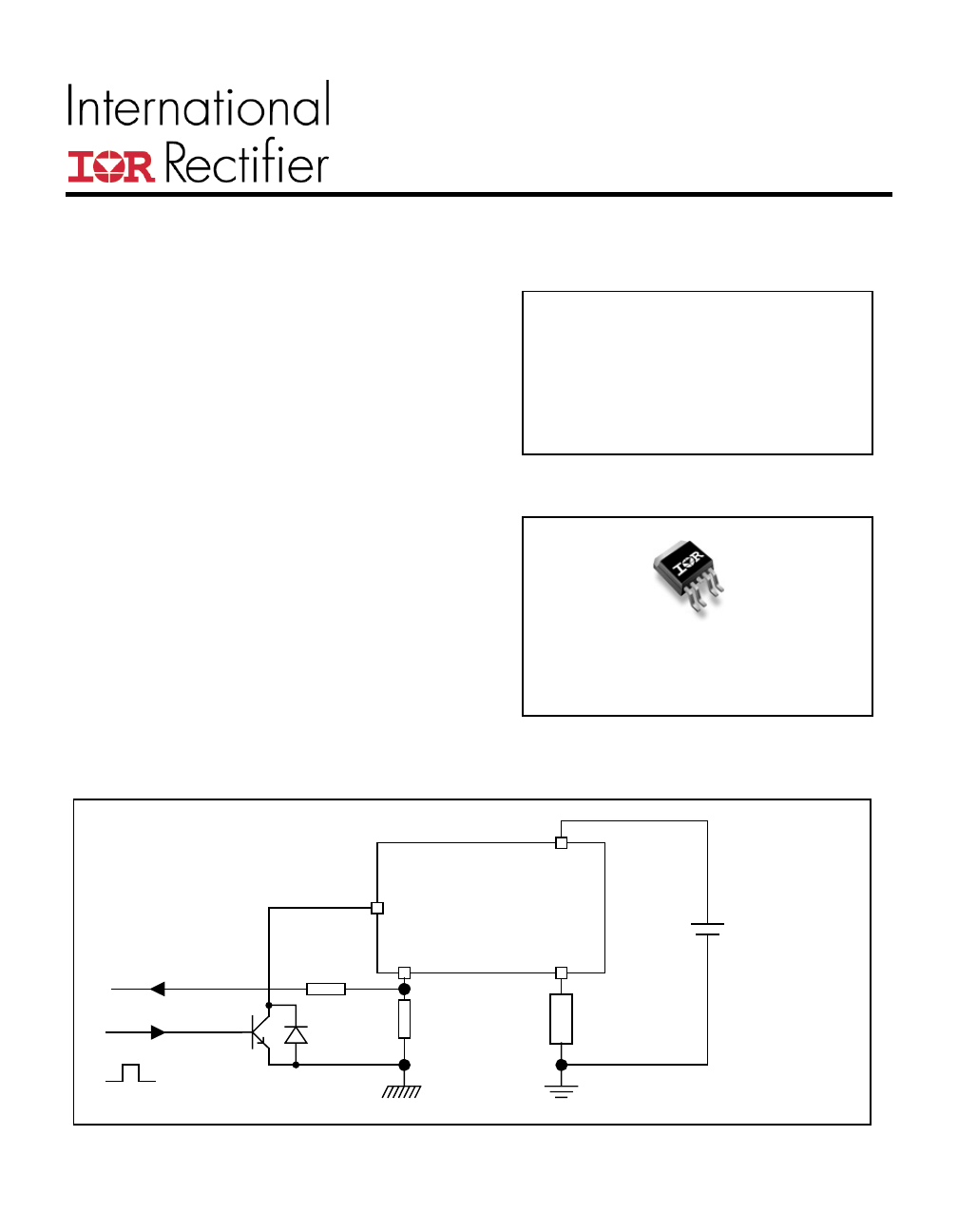
Typical Connection
Out
AUIPS7121R
IN
Rifb
Vcc
Load
Battery
Input
Power
Ground
Ifb
Logic
Ground
Current feeback
10k
On
Off
AUIPS7121R
Qualification Information
†
Automotive
(per AEC-Q100
††
)
Qualification Level
Comments: This family of ICs has passed an Automotive qualification.
IR’s Industrial and Consumer qualification level is granted by extension
of the higher Automotive level.
Moisture Sensitivity Level
DPAK-5L
MSL1,
260°C
(per IPC/JEDEC J-STD-020)
Machine Model
Class M2 (200 V)
(per AEC-Q100-003)
Human Body Model
Class H1C (1500 V)
(per AEC-Q100-002)
ESD
Charged Device Model
Class C5 (1000 V)
(per AEC-Q100-011)
IC Latch-Up Test
Class II, Level A
(per AEC-Q100-004)
RoHS Compliant
Yes
†
Qualification standards can be found at International Rectifier’s web site
http://www.irf.com/
††
Exceptions to AEC-Q100 requirements are noted in the qualification report.
www.irf.com
2
AUIPS7121R
Absolute Maximum Ratings
Absolute maximum ratings indicate sustained limits beyond which damage to the d
cur. (Tambient=25°C unless
otherwise specified).
arameter
evice may oc
Symbol P
Min.
Max.
Units
Vout
Maximum output voltage
Vcc-60 Vcc+0.3
V
Vcc-Vin max. Maximum Vcc voltage
-32
60
V
Iifb, max.
Maximum feedback current
-50
10
mA
Vcc sc
Maximum Vcc voltage with short circuit protection see page 7
V
⎯
50
Maximum power dissipation (internally limited
protection)
by thermal
Pd
Rth=50°C/W DPack 6cm² footprint
⎯
2.5
W
Tj max.
Max. storage & operating junction temperature
-40
150
°C
Thermal Characteristics
mbol
Max.
Units
Sy
Parameter
Typ.
Rth1
Thermal resistance junction to ambient DPak Std footprint
⎯
70
Rth2
tion to ambient Dpak 6cm² footprin
⎯
Thermal resistance junc
t
50
Rth3
Thermal resistance junction to case Dpak
⎯
°C/W
2
Recommended Operating Conditions
These values are given for a quick design.
S
Min.
Max.
Units
ymbol Parameter
Continuous output current, Tambient=85°C, Tj=125°C
I
⎯
3.8
A
out
Rth=50°C/W, Dpak 6cm² footprint
Rifb Ifb
resistor
1.5
⎯
k
Ω
www.irf.com
3
AUIPS7121R
Static Electrical Characteristics
meter
Min.
Typ.
Max.
Units
Test
Conditions
Tj=25°C, Vcc=28V (unless otherwise specified)
Symbol Para
Vcc op.
Operating voltage range
6
⎯
60 V
ON state resistance Tj=25°C
⎯
24 30
Rds(on)
150°C(2)
⎯
45 55
m
Ω
ON state resistance Tj=
Ids=2A
Icc off
Supply leakage current
⎯
2 4
Iout off
Output leakage current
⎯
2 4
µA
Vi
c=28
ifb=V
Vout=Vgnd
n=Vc
V,V
gnd
Iin on
mA
Vcc
in=28V
Input current when device on
1
2.5
4
-V
V clamp1
cc to Vout clamp voltage 1
Id=10mA
V
60
64
⎯
V clamp2
65
72
Id=20A see fig. 2
Vcc to Vout clamp voltage 2
60
Vih(1)
High level Input threshold voltage
⎯
3.5 5.9
Id=10mA
Vil(1)
Low level Input threshold voltage
1.5
3.2
⎯
V
Rds(on) rev
R
te resist
everse On sta
ance Tj=25°C
⎯
25 40 m
Ω
Isd=2A
F
.85
orward body diode voltage Tj=25°C
⎯
0.75 0
Vf
F
7
V
I
orward body diode voltage Tj=125°C
⎯
0.62 0.
f=3A
Rin In
0
Ω
put
resistor
180
250
35
(1) Input threshold
in and the tab.
Min.
Typ.
Max.
Units
o
n
s are measured directly between the input p
Switching Electrical Characteristics
Vcc=28V, Resistive load=6.8
Ω, Tj=25°C
P
Symbol arameter
Test
C nditio s
tdon
T
30
urn on delay time
6
15
tr
R
µs
ise time from 20% to 80% of Vcc
5
10
30
tdoff
Turn off delay time
25
50
100
tf
Fall time from 80% to 20% of Vcc
6
15
30
µs
See fig. 1
Protection Characteristics
Tj=25°C, Vcc=28V (unless otherwise specified)
Symbol Parameter
Min.
Typ.
Max.
Units
Test
Conditions
Tsd
Over temperature threshold(2)
150
165
⎯
°C
See fig. 3 and fig. 11
Isd
Over-current shutdown
50
60
80
A
See fig. 3 and page 7
I fault
Ifb after an over-current or an over-
temperature (latched)
2.7 3.3 4
mA
See fig. 3
Current Sensing Characteristics
Tj=25°C, Vcc=28V (unless otherwise specified), Vcc-Vifb>4V
Symbol Parameter
Min.
Typ.
Max.
Units
Test
Conditions
Ratio
I load / Ifb current ratio
7050
8500
9950
Iload=5A
Ratio_TC
I load / Ifb variation over temperature(2)
-5%
0
+5
%
Tj=-40°C to +150°C
I offset
Load current offset
-0.6
0
0.6
A
Iout<5A
Ifb leakage
Ifb leakage current
0
10
100
µA
Iout=0A
(2) Guaranteed by design
www.irf.com
4
AUIPS7121R
Lead Assignments
1- NC
2- In
- Vcc
3
4- Ifb
t
5- Ou
1 2 4 5
ak
Vcc
DP
3-
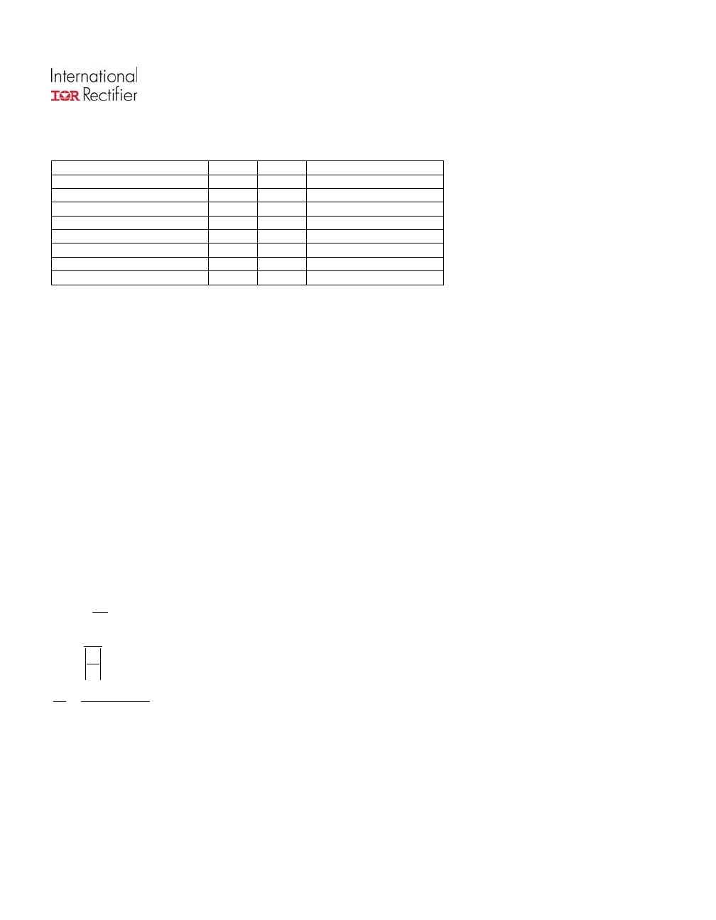
Functiona
All values are typ
l Block Diagram
ical
Diag
Charge
Pump
Driver
IFB OUT
VCC
75V
250
Ω
Tj > 165°C
Iout > 60A
60V
75V
-
+
75V
IN
Set
Reset
Latch
Q
1.5mA
3V
+
-
Reverse
Battery
Protection
www.irf.com
5
AUIPS7121R
Truth Table
Op. Conditions
Input
Output
Ifb pin voltage
Normal mode
H
L
0V
Normal mode
L
H
I load x Rfb / Ratio
Open load
H
L
0V
Open load
L
H
Ifb leakage x Rifb
Short circuit to GND
H
L
0V
Short circuit to GND
L
L
I fault x Rifb(latched)
Over temperature
H
L
0V
Over temperature
L
L
I fault x Rifb (latched)
Operating voltage
Maximum Vcc voltage : this is the maximum voltage before the breakdown of the IC process.
Operating voltage : This is the Vcc range in which the functionality of the part is guaranteed. The AEC-Q100 qualification
is run at the maximum operating voltage spe
cified in the datasheet.
Reverse battery
During the reverse battery the Mosfet is turned on if the input pin is powered with a diode in parallel of the input transistor.
Power dissipation in the IPS : P = Rdson rev * I load² + Vcc² / 250 ( internal input resistor ).
If the power dissipation is too high in Rifb, a diode in serial can be added to block the current.
Active clamp
The purpose of the active clamp is to limit the voltage across the MOSFET to a value below the body diode break down
voltage to reduce the amount of stress on the device during switching.
The temperature increase during active clamp can be estimated as follows:
)
t
(
Z
P
CLAMP
TH
CL
Tj
⋅
=
∆
Where:
)
t
(
Z
CLAMP
TH
is the thermal impedance at t
CLAMP
and can be read from the thermal impedance curves given in the
data sheets.
CLavg
CL
CL
I
V
P
⋅
=
: Power dissipation during active clamp
65V
V
CL
=
: Typical V
CLAMP
value
2
I
I
CL
CLavg
=
: Average current during active clamp
dt
di
I
t
CL
CL
=
: Active clamp duration
L
V
V
dt
di
CL
Battery
−
=
: Demagnetization current
Figure 9 gives the maximum inductance versus the load current in the worst case : the part switches off after an over
temperature detection. If the load inductance exceeds the curve, a free wheeling diode is required.
Over-current protection
The threshold of the over-current protection is set in order to guarantee that the device is able to turn on a load with an
inrush current lower than the minimum of Isd. Nevertheless for high current and high temperature the device may switch
off for a lower current due to the over-temperature protection. This behavior is shown in Figure 11.
www.irf.com
6
AUIPS7121R
Current sensing accuracy
Iout
Ifb
Ifb leakage
Ifb2
Ifb1
Iout1
I offset
Iout2
The current sensing is specified by measuring 3 points :
- Ifb1 for Iout1
- Ifb2 for Iout2
- Ifb leakage for Iout=0
the Ifb for any Iout value using :
, the accuracy of the system will depends on the variation of
Ratio_TC specified in page 4.
The Ioffset variation depends directly on the Rdson :
I offset@-40°C= I offset@25°C / 0.8
Maximum Vcc voltage with short circuit protection
The maximum Vcc voltage with short circuit is the maximum voltage for which the part is able to protect itself under test
conditions representative of the application. 2 kind of short circuits are considered : terminal and load short circuit.
L SC
R SC
The parameters in the datasheet are computed with the following formula :
Ratio = ( Iout2 – Iout1 )/( Ifb2 – Ifb1)
I offset = Ifb1 x Ratio – Iout1
This allows the designer to evaluate
Ifb = ( Iout + I offset ) / Ratio if Ifb > Ifb leakage
For some applications, a calibration is required. In that case
the I offset and the ratio over the temperature range. The ratio variation is given by
I offset@150°C= I offset@25°C / 1.9
Out
IPS
Vcc
L SC
L supply
5µH
R supply
10mohm
Terminal SC
0.1 µH
10 mohm
Load SC
10 µH
100 mohm
R SC
www.irf.com
7
AUIPS7121R
Tj
Tsd
165°C
Ids
Vin
I shutdown
Tshutdown
Vifb
V fault
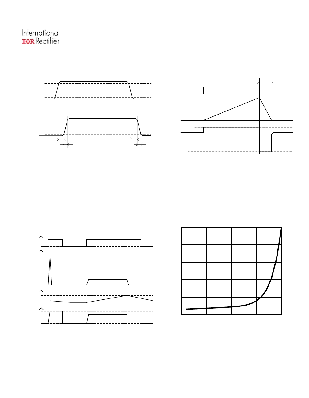
Figure 3 – Protection timing diagram
Vds
Ids
Vcc-Vin
Vout
Vcc-Vin
80%
20%
80%
20%
Td on
Tr
Td off
Tf
Vcc
Vds clamp
T clamp
See Application Notes to evaluate power dissipation
ctive clamp waveforms
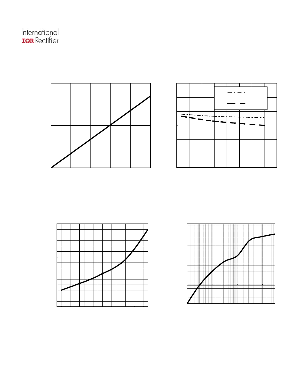
Figure 2 – A
Figure 1 – IN rise time & switching definitions
0
5
15
25
-
0
100
150
Tj, junction temperature (°C)
Figure 4 – Icc off (µA) Vs Tj (°C)
20
10
Icc off, supply leakage current (µA)
50
50
www.irf.com
8
AUIPS7121R
www.irf.com
9
Figure 8 – Transient thermal impedance (°C/W)
Vs time (s)
)
h
,
tr
a
n
s
ie
n
t
th
e
rm
a
l
im
p
e
d
a
n
c
e
(
°C
/W
Z
t
Time (s)
50%
100%
150%
-50
0
50
100
150
200%
Fig
C)
Tj, junction temperature (°C)
Rds(on), Drain-to-Source On Resistance
(Normalized)
ure 7 - Normalized Rds(on) (%) Vs Tj (°
1
2
3
4
5
6
VIH
VIL
0
-50
-25
0
25
50
75
100
125
150
Tj, junction temperature (°C)
Vih and Vil (V)
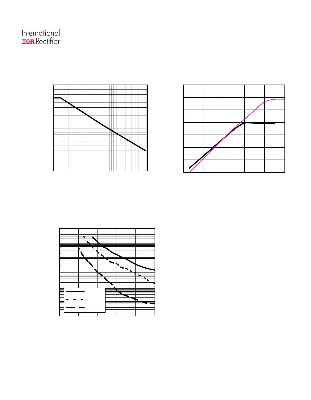
Figure 6 – Vih and Vil (V) Vs Tj (°C)
0
0
10
20
30
40
50
Vcc-Vin, supply voltage (V)
Iccoff, supply current (µA)
2
4
0.01
0.10
1.00
10.00
100.00
1.E-
05
1.E-
04
1.E-
03
1.E-
02
1.E-
01
1.E+0
0
1.E+0
1
1.E+0
2
Figure 5 – Icc off(µA) Vs Vcc-Vin (V)
AUIPS7121R
www.irf.com
10
0.0
0.2
0.4
0.6
0.8
1.0
1.2
1.4
0
2
4
6
8
25°C
150°C
1
10
100
1.E+01
1.E+02
1.E+03
1.E+04
Ifb, current feedback current (mA)
Max. output current (A)
10
Inductance (µH)
Iout, output current (A)
Fig
H)
ure 9 – Max. Iout (A) Vs inductance (µ
Figure 10 – Ifb (mA) Vs Iout (A)
Figure 11 – Tsd (s) Vs I out (A)
SMD with 6cm²
T
s
d
,
ti
m
e
t
o
s
h
u
td
o
w
n
(s
)
0.0001
0.001
0.01
0.1
1
10
100
0
10
20
30
40
'-40°C
'+25°C
'+125°C
50
Iout, output current (A)