
CGY41
IFAG IMM RPD D
1 of 6
Target DATASHEET
HiRel L- and S-Band GaAs General Purpose Amplifier
HiRel Discrete and Microwave Semiconductor
Single-stage monolithic microwave IC
(MMIC-amplifier )
Application range: 100 MHz to 3 GHz
Gain: 9.5 dB typ. @ 1.8 GHz
Low noise figure: 2.7 dB typ. @ 1.8 GHz
Bandwidth: 3 GHz typ. @ -3 dB, VSWR < 2 : 1 *
Operating voltage range: 3 to 5.5 V
Input and output matched to 50
Individual current control with neg. gate bias
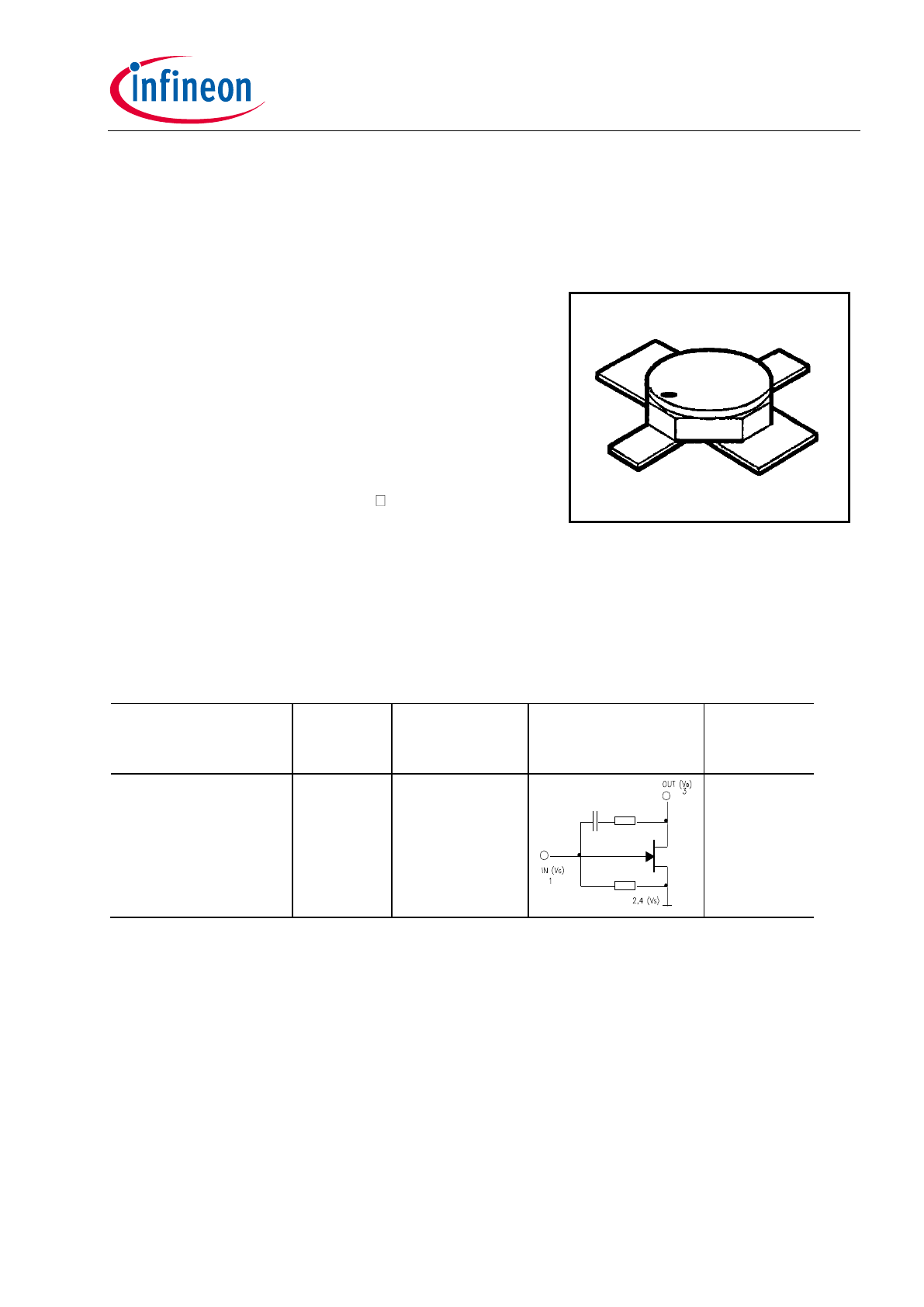
Hermetically sealed ceramic package micro-x
ESD:
Electrostatic discharge sensitive device,
observe handling precautions!
Type
Marking
Ordering Code Circuit Diagram
(Pin Configuration)
Package
CGY41 (ql)
-
see below
Micro-X
(ql) Quality Level:
P: Professional Quality,
Ordering Code:
on request
H: High Rel Quality,
Ordering Code:
on request
S: Space Quality,
Ordering Code:
on request
(see order instructions for ordering example)
1
2
3
4
CGY41
IFAG IMM RPD D
2 of 6
Target DATASHEET
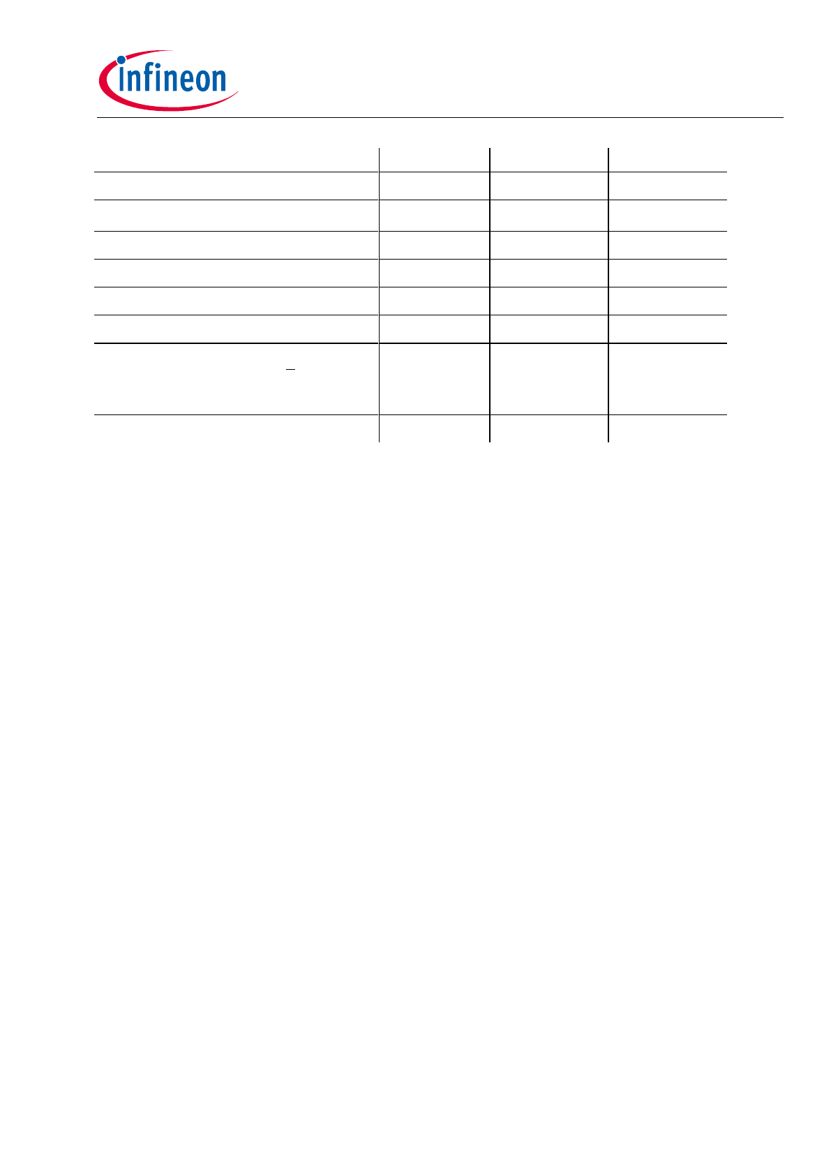
Maximum ratings
Symbol
Value
Unit
Drain-voltage
V
D
5.5
V
Gate-voltage
V
G
-4 ... 0.5
V
Drain-gate voltage
V
DG
9.5
V
RF Input power
1)
P
RFIN
16
dBm
Channel temperature
T
Ch
175
°C
Storage temperature range
T
stg
-55...+175
°C
Total power dissipation (T
S
< 82°C)
2)
P
tot
440
mW
Thermal resistance
Channel-soldering point
2)
R
thChS
160
K/W
Notes: Exceeding any of the max. ratings may cause permanent damage to the device. Appropriate
handling is required to protect the electrostatic sensitive MMIC against degradation due to excess
voltage or current spikes. Proper ground connection of leads 2 and 4 ( with min. inductance ) is required
to achieve the guaranteed RF performance, stable operating conditions and adequate cooling.
1) @ V
D
> 4.5 V derating required.
2) Ts is measured on the source lead at the soldering point to the PCB.
CGY41
IFAG IMM RPD D
3 of 6
Target DATASHEET
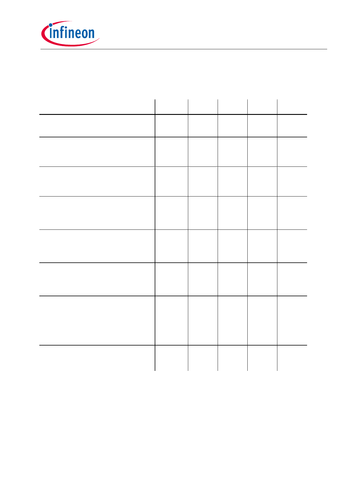
Electrical Characteristics
T
A
= 25 °C, V
G
= 0 V, V
D
= 4.5 V, R
S
= R
L
= 50
Ω unless otherwise specified
(for application circuit see next page)
Characteristics
Symbol
min
typ
max
Unit
Drain current
I
DSS
40
60
80
mA
Power gain
f = 200 MHz
f = 1800 MHz
G
9.5
8.5
10.5
9.5
13
11
dB
Gain flatness
f = 200 to 1000 MHz
f = 800 to 1800 MHz
GF
-
-
0.4
1.1
-
2
dB
Noise figure
f = 200 to 1000 MHz
f = 800 to 1800 MHz
F
-
-
2.5
2.7
-
4.0
dB
Input return loss
f = 200 to 1000 MHz
f = 800 to 1800 MHz
RL
IN
-
-
13
12
-
9.5
dB
Output return loss
f = 200 to 1000 MHz
f = 800 to 1800 MHz
RL
OUT
-
-
12
12
-
9.5
dB
Third order intercept point
Two tone intermodulation test
f
1
= 806 MHz, f
2
= 810 MHz
P
0
= 10 dBm ( both carriers )
IP3
31
32
-
dBm
1dB gain compression
f = 200 to 1800 MHz
P
1 dB
-
18
-
dBm
CGY41
IFAG IMM RPD D
4 of 6
Target DATASHEET
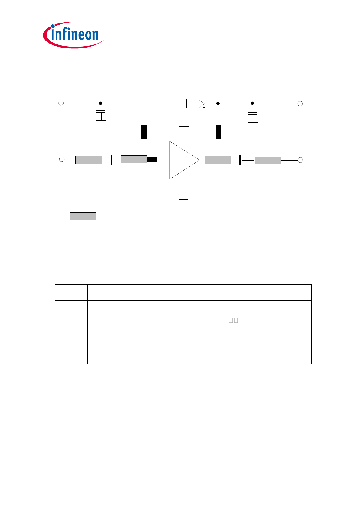
Application Circuit ( f = 800 to 1800 MHz )
CGY41
50 Ohm Microstripline
Input
50Ohm
Output
50Ohm
3
2
V
D
1
V
G
1
L
C
C
3
L
2
2
C
C
4
4
1
D
L
3
Legend of components
C
1
, C
2
C
3
, C
4
Chip capacitors 100 pF
Chip capacitors 1 nF
L
1
For optimized input matching
- discrete inductor: approx. 3nH, or
- printed microstripline inductor: Z approx. 100
l
e
approx. 5 mm
L
2
, L
3
- discrete inductor: approx. 40 nH, as e.g. 5 turns 0.25 mm copper
wire on nylon rod with M3-thread, or
- printed microstripline inductor
D
Z diode 5.6 V ( type BZW 22 C5 V 6 )
CGY41
IFAG IMM RPD D
5 of 6
Target DATASHEET
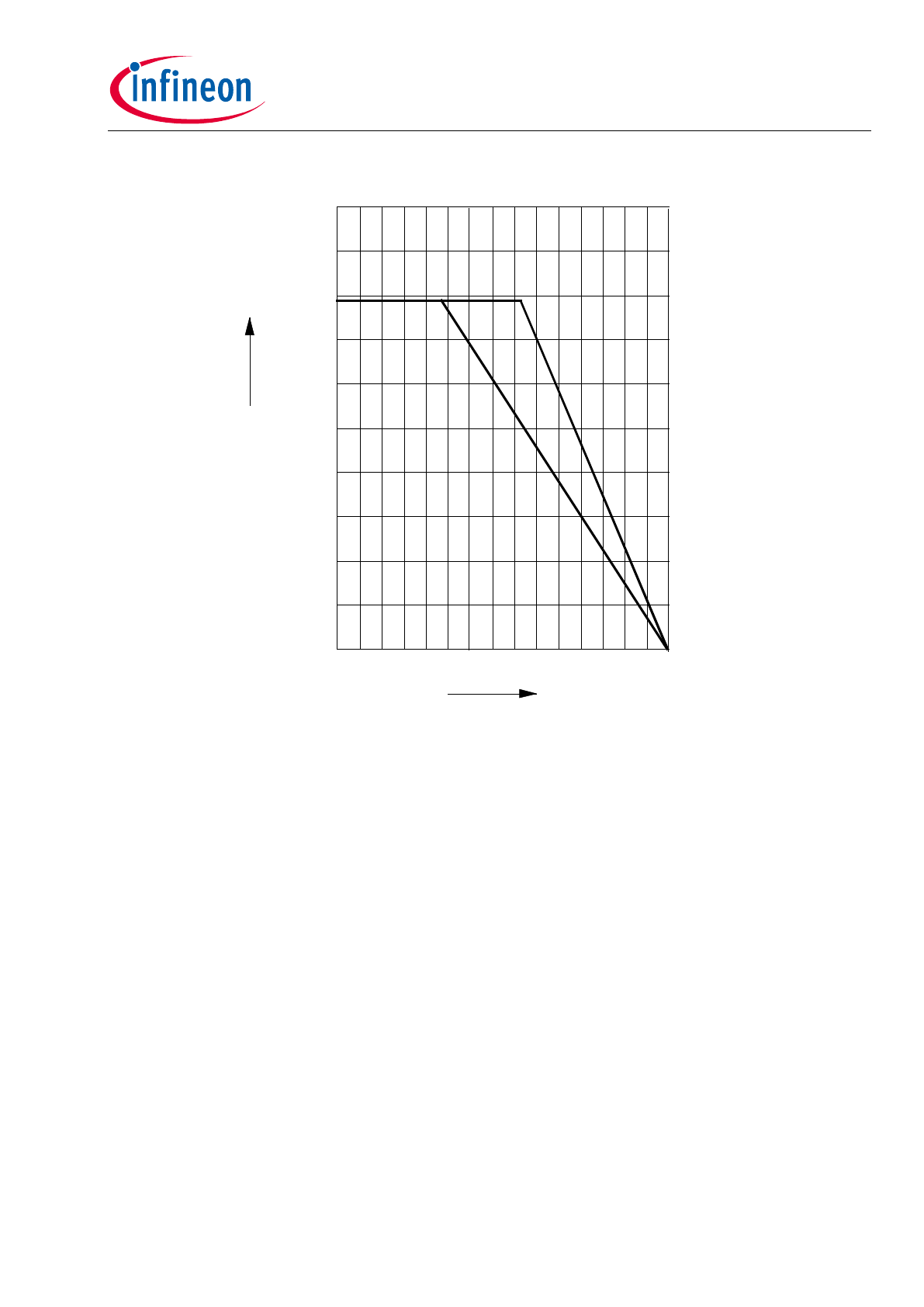
Total Power Dissipation P
tot
= f (T
S
;T
A
)
0
0 50 100
150
A
S
tot
P
T
T
;
[ °C ]
[ mW ]
A
T
S
T
100
200
300
400
500
CGY41
IFAG IMM RPD D
6 of 6
Target DATASHEET
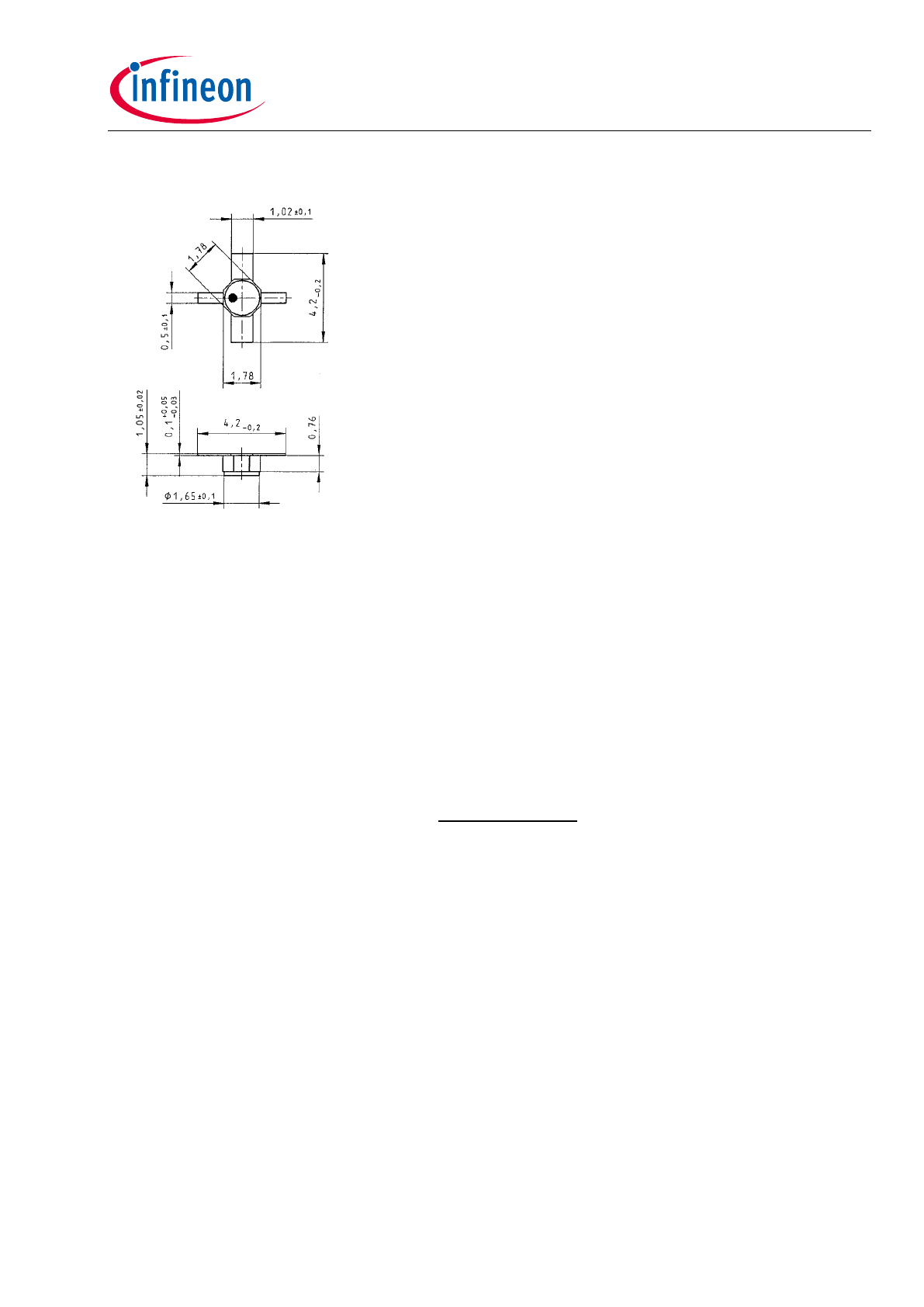
Micro-X Package
Edition 2011-02
Published by
Infineon Technologies AG
85579 Neubiberg, Germany
© Infineon Technologies AG 2011
All Rights Reserved.
Attention please!
The information given in this document shall in no event be regarded as a guarantee of
conditions or characteristics
(“Beschaffenheitsgarantie“). With respect to any examples or
hints given herein, any typical values stated herein and/or any information regarding the
application of the device, Infineon Technologies hereby disclaims any and all warranties and
liabilities of any kind, including without limitation warranties of non-infringement of intellectual
property rights of an third party.
Information
For further information on technology, delivery terms and conditions and prices please contact
your nearest Infineon Technologies Office (www.infineon.com).
Warnings
Due to technical requirements components may contain dangerous substances. For
information on the types in question please contact your nearest Infineon Technologies Office.
Infineon Technologies Components may only be used in life-support devices or systems with
the express written approval of Infineon Technologies, if a failure of such components can
reasonably be expected to cause the failure of that life-support device or system, or to affect
the safety or effectiveness of that device or system.
Life support devices or systems are intended to be implanted in the human body, or to support
and/or maintain and sustain and/or protect human life. If they fail, it is reasonable to assume
that the health of the user or other persons may be endangered.
1
2
3
4