
Data Sheet
1
V1.1, 2007-09-25
Smart High-Side Power Switch
BTS723GW
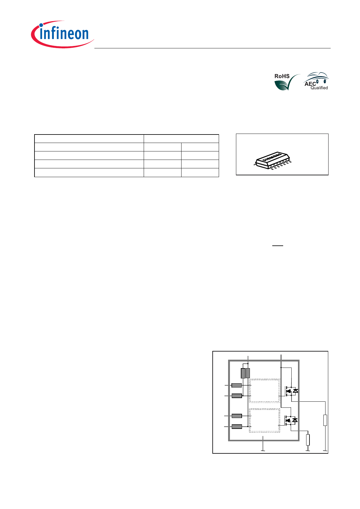
7ZR&KDQQHOV[PΩ
6WDWXV)HHGEDFN
6XLWDEOHIRU9
Product Summary Package
2SHUDWLQJ9ROWDJH
9
EERQ
9
$FWLYHFKDQQHOV 2QH
WZRSDUDOOHO
2QVWDWH5HVLVWDQFH
5
21
PΩ
PΩ
1RPLQDOORDGFXUUHQW
,
/120
$
$
&XUUHQWOLPLWDWLRQ
,
/6&U
$
$
*HQHUDO'HVFULSWLRQ
• 1FKDQQHOYHUWLFDOSRZHU026)(7ZLWKFKDUJHSXPSJURXQGUHIHUHQFHG&026FRPSDWLEOHLQSXWDQG
GLDJQRVWLFIHHGEDFNPRQROLWKLFDOO\LQWHJUDWHGLQ6PDUW6,3026
9WHFKQRORJ\
• 3URYLGLQJHPEHGGHGSURWHFWLYHIXQFWLRQV
• $QDUUD\RIUHVLVWRUVLVLQWHJUDWHGLQRUGHUWRUHGXFHWKHH[WHUQDOFRPSRQHQWV
$SSOLFDWLRQV
• &FRPSDWLEOHKLJKVLGHSRZHUVZLWFKZLWKGLDJQRVWLFIHHGEDFNIRU9DQG9DQG9JURXQGHGORDGV
• $OOW\SHVRIUHVLVWLYHLQGXFWLYHDQGFDSDFLWLYHORDGV
• 0RVWVXLWDEOHIRULQGXFWLYHORDGV
• 5HSODFHVHOHFWURPHFKDQLFDOUHOD\VIXVHVDQGGLVFUHWHFLUFXLWV
%DVLF)XQFWLRQV
• &026FRPSDWLEOHLQSXW
• ,PSURYHGHOHFWURPDJQHWLFFRPSDWLELOLW\(0&
• )DVWGHPDJQHWL]DWLRQRILQGXFWLYHORDGV
• 6WDEOHEHKDYLRXUDWXQGHUYROWDJH
• :LGHRSHUDWLQJYROWDJHUDQJH
• /RJLFJURXQGLQGHSHQGHQWIURPORDGJURXQG
• 2SWLPL]HGLQYHUVFXUUHQWFDSDELOLW\
3URWHFWLRQ)XQFWLRQV
• 6KRUWFLUFXLWSURWHFWLRQ
• 2YHUORDGSURWHFWLRQ
• &XUUHQWOLPLWDWLRQ
• 7KHUPDOVKXWGRZQ
• 2YHUYROWDJHSURWHFWLRQLQFOXGLQJORDGGXPSZLWKH[WHUQDO
UHVLVWRU
• 5HYHUVHEDWWHU\SURWHFWLRQZLWKH[WHUQDOUHVLVWRU
• /RVVRIJURXQGDQGORVVRI9
EE
SURWHFWLRQ
• (OHFWURVWDWLFGLVFKDUJHSURWHFWLRQ(6'
'LDJQRVWLF)XQFWLRQ
• 'LDJQRVWLFIHHGEDFNZLWKRSHQGUDLQRXWSXWDQGLQWHJUDWHG
SXOOXSUHVLVWRUV
• 2SHQORDGGHWHFWLRQLQ2))VWDWH
• )HHGEDFNRIWKHUPDOVKXWGRZQLQ21VWDWH
• 'LDJQRVWLFIHHGEDFNRIERWKFKDQQHOVZRUNVSURSHUO\LQFDVHRILQYHUVHFXUUHQW
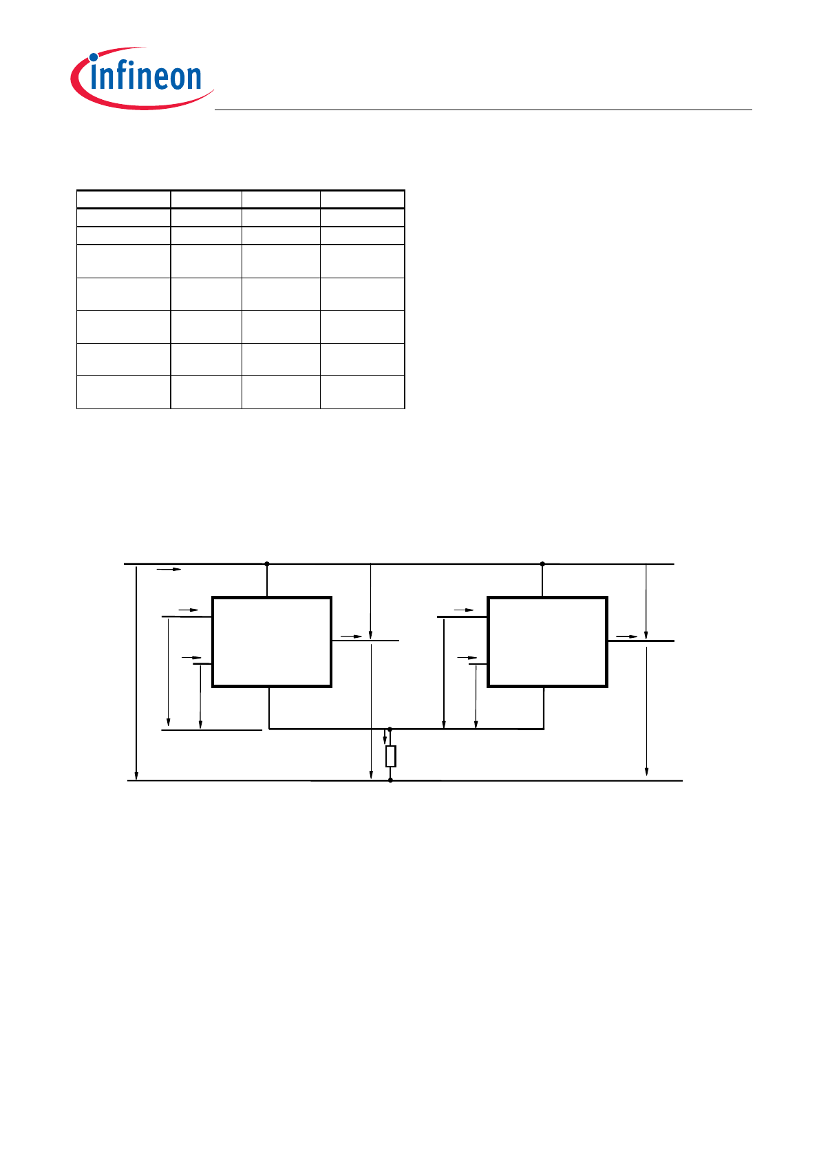
Block Diagram
P-DSO-14
9EE
/RJLF
&KDQQHO
,1
67
,1
67
*1'
/RDG
/RDG
352)(7
287
287
/RJLF
&KDQQHO
6WDWXVSXOO
XSYROWDJH
PG-DSO14
Data Sheet
2
V1.1, 2007-09-25
Smart High-Side Power Switch
BTS723GW
)XQFWLRQDOGLDJUDP
)XQFWLRQVDQG&RPSRQHQWVRI
LQSXWORJLFDQGJDWHFRQWURO
(6'SURWHFWLRQ
&KDUJHSXPSOHYHOVKLIWHU
UHFWLILHU
*DWHSURWHFWLRQ
&XUUHQWOLPLW
/LPLWIRUXQFODPSHG
LQGXFWLYHORDGV
)XQFWLRQDQGFRPSRQHQWVRI
RXWSXWORJLF
2SHQORDGGHWHFWLRQ
6KRUWFLUFXLWGHWHFWLRQ
7HPSHUDWXUHVHQVRU
6WDWXV
)XQFWLRQVHHWUXWKWDEOH
)XQFWLRQDQGFRPSRQHQWVRI
LQSXWORJLFDQGJDWHFRQWURO
HTXLYDOHQWWRFKDQQHORQH
)XQFWLRQDQGFRPSRQHQWVRI
RXWSXWORJLFHTXLYDOHQWWR
FKDQQHORQH
6WDWXV
)XQFWLRQ VHH WUXWKWDEOH
,1
352)(7
9
EE
/HDGIUDPH
287
/RDG*1'
/RDG
/RDG
287
/RDG*1'
6383LQIRUH[WHUQDO3XOO8S9ROWDJH
67
/RJLF*1'
67
,1
/RJLFFKDQQHORQH
/RJLFFKDQQHOWZR
9
EE
5 NΩ
5 NΩ
5 Ω
5 NΩ
5 Ω
Data Sheet
3
V1.1, 2007-09-25
Smart High-Side Power Switch
BTS723GW
Pin Definitions and Functions
Pin
Symbol
Function
1,7,
8,14,
V
bb
Positive power supply voltage. Design the
wiring for the simultaneous max. short circuit
currents from channel 1 to 2 and also for low
thermal resistance
2 IN1
6 IN2
Input 1,2 activates channel 1,2 in case
of logic high signal
12,13 OUT1
9,10 OUT2
Output 1,2 protected high-side power output
of channel 1,2. Design the wiring for the max.
short circuit current; both outputpins have to be
connected in parallel for operation according
this spec.
3 ST1
5 ST2
Diagnostic feedback 1,2 of channel 1,2
open drain
4 GND
Logic Ground
11 SPU
Connection for external pull up voltage source
for the open drain status output.
Pull up resistors are integrated.
Pin configuration
(top view)
V
bb
1
•
14 V
bb
IN1 2
13 OUT1
ST1 3
12 OUT1
GND 4
11 SPU
ST2 5
10 OUT2
IN2 6
9 OUT2
V
bb
7
8 V
bb

Data Sheet
4
V1.1, 2007-09-25
Smart High-Side Power Switch
BTS723GW
Parameter Symbol
Values
Unit
Supply voltage (overvoltage protection see page 6)
V
bb
58
V
Supply voltage for full short circuit protection
T
j,start
= -40 ...+150°C
V
bb
50
V
Output Voltage to V
bb
V
ON
70
V
Negative voltage slope at output
-d
V
OUT
/d
t
20
V/µs
Load current (Short-circuit current, see page 7)
I
L
I
L(LIM)
1
)
A
Load dump protection
2
)
V
LoadDump
=
V
A
+
V
s
,
V
A
= 27 V
R
I
3
)
= 8
Ω, t
d
= 200 ms; IN = low or high,
each channel loaded with
R
L
= 20
Ω,
V
Load dump
4
)
70
V
Operating temperature range
Storage temperature range
T
j
T
stg
-40 ...+150
-55 ...+150
°C
Power dissipation (DC)
5)
T
a
= 25°C:
(all channels active)
T
a
= 85°C:
P
tot
3.0
1.6
W
Maximal switchable inductance, single pulse
V
bb
= 12V,
T
j,start
= 150°C
5)
,
I
L
= 2.5 A,
E
AS
= 110 mJ, 0
Ω one
channel:
I
L
= 3.5 A,
E
AS
= 278 mJ, 0
Ω
two parallel channels:
see diagrams on page 12
Z
L
23.0
30.0
mH
Electrostatic discharge capability (ESD):
(Human Body Model) acc. MIL-STD883D, method 3015.7 and ESD
assn. std. S5.1-1993 R=1.5k
Ω; C=100pF
V
ESD
1.0
kV
Input voltage (DC)
V
IN
±42
V
Current through input pin (DC)
Current through status pin (DC)
I
IN
I
ST
±2.0
±2.0
mA
Status pull up voltage
V
SPU
±42
V
1
) Current limit is a protection function. Operation in current limitation is considered as "outside" normal
operating range. Protection functions are not designed for continuous repetitive operation.
2
) Supply voltages higher than V
bb(AZ)
require an external current limit for the GND and status pins (a 150
Ω
resistor for the GND connection is recommended.
3)
R
I
= internal resistance of the load dump test pulse generator
4)
V
Load dump
is setup without the DUT connected to the generator per ISO 7637-1 and DIN 40839
5
) Device on 50mm*50mm*1.5mm epoxy PCB FR4 with 6cm
2
(one layer, 70
µm thick) copper area for Vbb
connection. PCB is vertical without blown air. See page 15
Data Sheet
5
V1.1, 2007-09-25
Smart High-Side Power Switch
BTS723GW
Parameter and Conditions
Symbol
Values
Unit
min typ
Max
Thermal resistance
junction - soldering point
5),6)
each
channel:
R
thjs
-- --
25
K/W
junction - ambient
5)
one channel active:
all channels active:
R
thja
--
--
45
41
--
--
6
) Soldering point: Upper side of solder edge of device pin 15. See page 15
Electrical Characteristics
Parameter and Conditions,
each of the two channels
Symbol
Values
Unit
at T
j
= -40...+150°C,
V
bb
= 24 V unless otherwise specified
min typ
Max
Load Switching Capabilities and Characteristics
On-state resistance (Vbb to OUT);
IL = 2 A, V
bb
≥ 7V
each channel,
T
j
= 25°C:
T
j
= 150°C:
two parallel channels,
T
j
= 25°C:
see diagram, page 12
R
ON
--
--
--
90
170
45
105
210
53
m
Ω

Data Sheet
6
V1.1, 2007-09-25
Smart High-Side Power Switch
BTS723GW
Parameter and Conditions,
each of the two channels
Symbol
Values
Unit
at T
j
= -40...+150°C,
V
bb
= 24 V unless otherwise specified
min typ
Max
Nominal load current
one channel active:
two parallel channels active:
Device on PCB
7
), Ta = 85°C, Tj ≤ 150°C
I
L(NOM)
2.5
4.0
2.9
4.2
--
--
A
Output current
while GND disconnected or pulled up
8
)
;
Vbb = 30 V, VIN = 0,
see diagram page 11
I
L(GNDhigh)
-- --
1.0
mA
Turn-on time
9
)
IN
to 90%
V
OUT
:
Turn-off time
IN
to 10%
V
OUT
:
R
L
= 12
Ω
t
on
t
off
--
--
--
--
55
95
µs
Slew rate on
9
)
10 to 30%
V
OUT
,
R
L
= 12
Ω:
d
V
/d
t
on
1.0 -- 5
V/
µs
Slew rate off
9
)
70 to 40%
V
OUT
,
R
L
= 12
Ω:
-d
V
/d
t
off
1.0 -- 5
V/
µs
Operating Parameters
Operating voltage
V
bb(on)
7.0
--
58
V
Undervoltage restart of charge pump
T
j
=-40...+25°C:
T
j
=+150°C:
V
bb(ucp)
--
--
4
--
5.5
7.0
V
Overvoltage protection
10
)
I
bb
= 40 mA
V
bb(AZ)
58.5 63 69
V
Standby current
11
)
T
j
=-40°C...+25°C
:
T
j
=+125°C
12
)
:
V
IN
= 0;
see diagram page 10
T
j
=+150°C:
I
bb(off)
--
--
--
13
25
23
23
35
µA
Off-State output current (included in
I
bb(off)
)
V
IN
= 0; each channel
I
L(off)
-- 3 --
µA
Operating current
13)
,
V
IN
= 5V,
one channel on:
all channels on:
I
GND
--
--
1.0
2.0
1.5
3.0
mA
7
) Device on 50mm*50mm*1.5mm epoxy PCB FR4 with 6cm
2
(one layer, 70
µm thick) copper area for Vbb
connection. PCB is vertical without blown air. See page 15
8
) not subject to production test, specified by design
9
) See timing diagram on page 13.
10
) Supply voltages higher than V
bb(AZ)
require an external current limit for the GND; a 150
Ω resistor is
recommended. See also
V
ON(CL)
in table of protection functions and circuit diagram on page 10.
11
) Measured with load; for the whole device; all channels off
12
) not subject to production test, specified by design
13
) Add I
ST
, if
I
ST
> 0

Data Sheet
7
V1.1, 2007-09-25
Smart High-Side Power Switch
BTS723GW
Parameter and Conditions,
each of the two channels
Symbol
Values
Unit
at T
j
= -40...+150°C,
V
bb
= 24 V unless otherwise specified
min typ
Max
Protection Functions
14)
Current limit,
(see timing diagrams, page 13)
T
j
=-40°C:
T
j
=25°C:
T
j
=+150°C:
I
L(lim)
--
--
5
10
9
8
12
--
--
A
Repetitive short circuit current limit
15
)
,
T
j
=
T
jt
each channel
two parallel channels
(see timing diagrams, page 13)
I
L(SCr)
--
--
8
8
--
--
A
Initial short circuit shutdown time
T
j,start
=25°C:
(see timing diagrams on page 13)
t
off(SC)
--
2
--
ms
Output clamp (inductive load switch off)
16)
at VON(CL) = Vbb - VOUT
,
IL = 1 A
V
ON(CL)
59
64 70
V
Thermal overload trip temperature
T
jt
150 -- --
°C
Thermal hysteresis
∆T
jt
-- 10 --
K
Reverse Battery
Reverse battery voltage
17
)
-
V
bb
--
--
24
V
Drain-source diode voltage
(V
out
> V
bb
)
18
)
I
L
= - 3.0 A,
T
j
= +150°C
-
V
ON
--
650
--
mV
Inverse current
19
)
GND current in case of 3A inverse current
20
)
I
GND(inv cur)
-- --
15
mA
14
) Integrated protection functions are designed to prevent IC destruction under fault conditions described in the
data sheet. Fault conditions are considered as "outside" normal operating range. Protection functions are not
designed for continuous repetitive operation.
15
) not subject to production test, specified by design
16
) If channels are connected in parallel, output clamp is usually accomplished by the channel with the lowest
V
ON(CL)
17
) Requires a 150 Ω resistor in GND connection. The reverse load current through the intrinsic drain-source
diode has to be limited by the connected load. Power dissipation is higher compared to normal operating
conditions due to the voltage drop across the drain-source diode. The temperature protection is not active
during reverse current operation! Input and Status currents have to be limited (see max. ratings page 4 and
circuit page 10).
18
) not subject to production test, specified by design
19
) not subject to production test, specified by design
20
) In case of an inverse current of 3A the both status outputs must not be disturbed.
The neighbour channel can be switched normally; not all paramters lay within the range of the spec
Please note, that in case of an inverse current no protection function is active. The power dissipation is
higher compared to normal operation in forward mode due to the voltage drop across the drain-source diode
Data Sheet
8
V1.1, 2007-09-25
Smart High-Side Power Switch
BTS723GW
Parameter and Conditions,
each of the two channels
Symbol
Values
Unit
at T
j
= -40...+150°C,
V
bb
= 24 V unless otherwise specified
min typ
Max
Diagnostic Characteristics
Open load detection current
21
)
I
L(off)
-- 3
--
µA
Open load detection voltage
V
OUT(OL)
2.0 2.85
3.7
V
Short circuit detection voltage
22
)
V
bb
(pin 1,7,8,14) to OUT1 (pin 12,13) resp.
V
bb
(pin 1,7,8,14) to OUT2 ( pin 9,10)
V
ON(SC)
--
4.0 --
V
Input and Status Feedback
23
)
Integrated resistors;
T
j
=25°C:
Input
(see circuit page 2)
Status
Status pull up
R
I
R
ST
R
pull up
--
0.53
--
20
0.85
12
--
1.2
--
k
Ω
k
Ω
k
Ω
Input turn-on threshold voltage
V
IN(T+)
1.2 --
2.2
V
Input turn-off threshold voltage
V
IN(T-)
1.0 -- --
V
Input threshold hysteresis
∆ V
IN(T)
-- 0.25
--
V
Off state input current
V
IN
= 0.4 V:
I
IN(off)
1
-- 15
µA
On state input current
V
IN
= 5 V:
I
IN(on)
10 25 50
µA
Status output (open drain)
Zener limit voltage
Status low voltage
V
SPU
= 5V:
V
ST(high)
V
ST(low)
5.4
--
6.1
--
--
0.4
V
21
) not subject to production test, specified by design
22
) not subject to production test, specified by design
23
) If a ground resistor R
GND
is used, add the voltage drop across these resistors.
Data Sheet
9
V1.1, 2007-09-25
Smart High-Side Power Switch
BTS723GW
Truth Table
Channel 1
Input 1
Output 1
Status 1
Channel 2
Input 2
Output 2
Status 2
level
level
BTS 723
Normal
operation
L
H
L
H
L
H
Open load
L
H
V
OUT
> 2.7V
H
H
H
Short circuit
to GND
L
H
L
L
L
L
Short circuit
to V
bb
L
H
H
H
H
H
Overtem-
perature
L
H
L
L
L
L
Parallel switching of channel 1 and 2 is easily possible by connecting the inputs and outputs in parallel. In this
mode it is recommended to use only one status.
Terms
352)(7
,1
67
287
*1'
9EE
967
9 ,1
,,1
9EE
,/
9287
, *1'
921
/HDGIUDPH
,EE
,67
5 *1'
&KDQQHO
352)(7
,1
67
287
*1'
9EE
967
9 ,1
,,1
,/
9287
921
/HDGIUDPH
,67
&KDQQHO
Leadframe (V
bb
) is connected to pin 1,7,8,14
External R
GND
optional; a single resistor R
GND
= 150
Ω for reverse battery protection up to the max.
operating voltage.
Data Sheet
10
V1.1, 2007-09-25
Smart High-Side Power Switch
BTS723GW
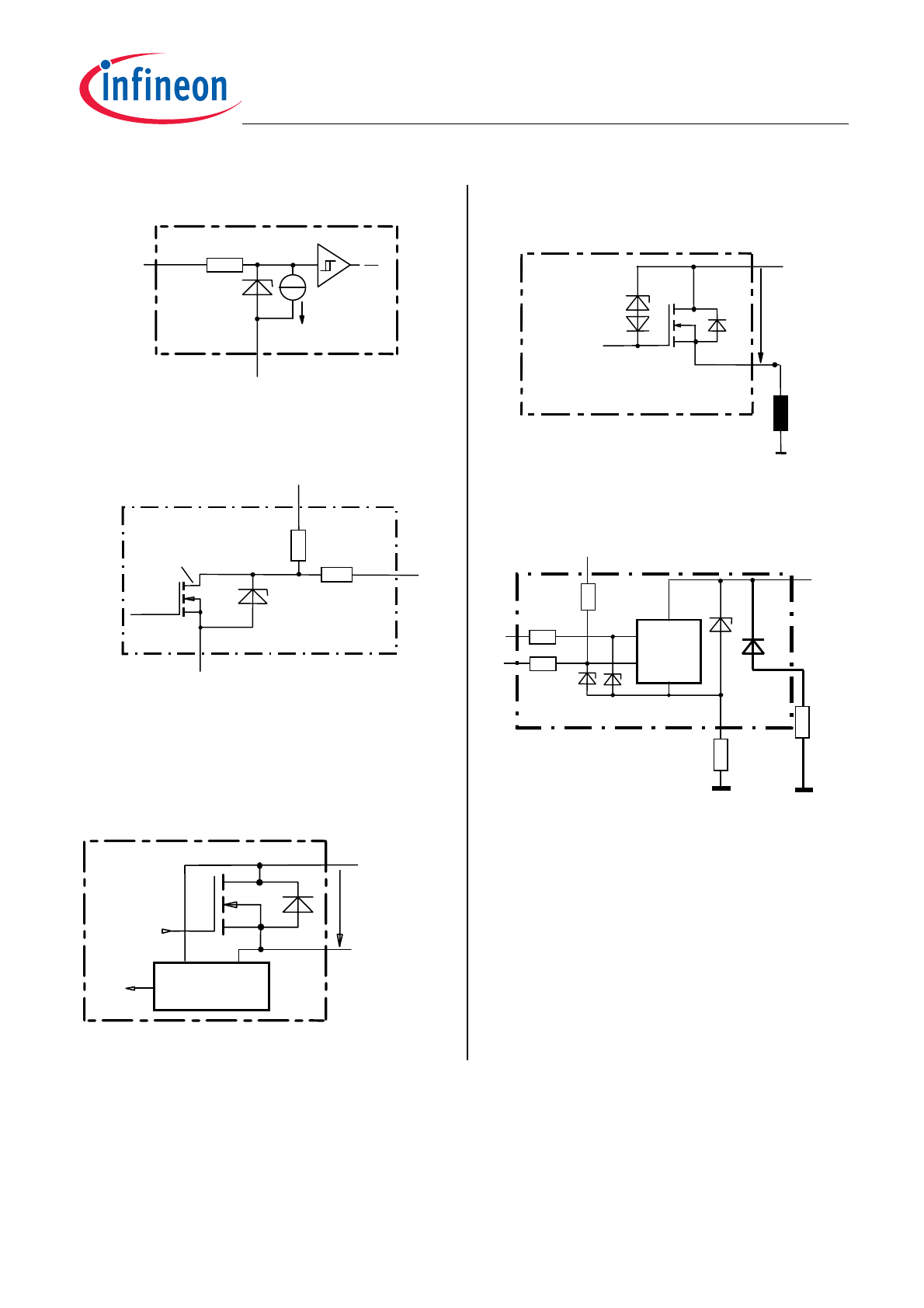
Input circuit (ESD protection),
IN1 or IN2
,1
*1'
,
5
(6'='
,,
,
The use of ESD zener diodes as voltage clamp at DC
conditions is not recommended.
Status output,
ST1 or ST2
67
*1'
(6'
='
6WDWXV3XOO8S9ROWDJH
5
6721
5
67
5
3XOOXS
ESD-Zener diode: 6.1 V typ., R
ST(ON)
< 250
Ω,
R
ST
= 850
Ω typ., R
pull up
= 12 k
Ω typ.
The use of ESD zener diodes as voltage clamp at DC
conditions is not recommended
Short Circuit detection
Fault Signal at ST-Pin:
V
ON
> 4.0 V typ, no switch off by
the PROFET itself, external switch off recommended!
6KRUWFLUFXLW
GHWHFWLRQ
/RJLF
XQLW
9EE
287
9
21
Inductive and overvoltage output clamp,
OUT1 or OUT2
9EE
287
9=
9
21
3RZHU*1'
V
ON
clamped to
V
ON(CL)
= 64 V typ.
Overvolt. and reverse batt. protection
9EE
,1
67
67
5
*1'
*1'
5
6LJQDO*1'
/RJLF
352)(7
9=
,
5
9=
/RDG*1'
/RDG
5
287
6WDWXVSXXOXS
5
6WDWXVSXOOXSYROWDJH
V
Z1
= 6.1 V typ.,
V
Z2
= 63 V typ.,
R
GND
= 150
Ω,
R
I
= 850
Ω W\S, R
ST
= 20 k
Ω typ., R
pull up
= 12 k
Ω typ
In case of reverse battery the load current has to be
limited by the load. Temperature protection is not
active