

Automotive Power
Data Sheet
Rev 1.3, 2010-03-16
Smart High-Side Power Switch
Smart High-Side Power Switch
PROFET BTS712N1
Data Sheet
2
Rev 1.3, 2010-03-16
Smart High-Side Power Switch
BTS712N1
Smart Four Channel Highside Power Switch
Features
•
Overload protection
•
Current limitation
•
Short-circuit protection
•
Thermal shutdown
•
Overvoltage protection
(including load dump)
•
Fast demagnetization of inductive loads
•
Reverse battery protection
1)
•
Undervoltage and overvoltage shutdown
with auto-restart and hysteresis
•
Open drain diagnostic output
•
Open load detection in OFF-state
•
CMOS compatible input
•
Loss of ground and loss of V
bb
protection
•
Electrostatic discharge (ESD) protection
Application
• µ
C compatible power switch with diagnostic feedback
for 12 V and 24 V DC grounded loads
•
All types of resistive, inductive and capacitive loads
•
Replaces electromechanical relays and discrete circuits
General Description
N channel vertical power FET with charge pump, ground referenced CMOS compatible input and diagnostic
feedback, monolithically integrated in Smart SIPMOS
technology.
Providing embedded protective functions.
Pin Definitions and Functions
Pin
Symbol
Function
1,10,
11,12,
15,16,
19,20
V
bb
Positive power supply voltage. Design the
wiring for the simultaneous max. short circuit
currents from channel 1 to 4 and also for low
thermal resistance
3 IN1
Input 1 .. 4, activates channel 1 .. 4 in case of
5
IN2
logic high signal
7 IN3
9 IN4
18 OUT1
Output 1 .. 4, protected high-side power output
17
OUT2
of channel 1 .. 4. Design the wiring for the
14
OUT3
max. short circuit current
13 OUT4
4 ST1/2
Diagnostic feedback 1/2 of channel 1 and
channel 2, open drain, low on failure
8 ST3/4
Diagnostic feedback 3/4 of channel 3 and
channel 4, open drain, low on failure
2 GND1/2
Ground 1/2 of chip 1 (channel 1 and channel 2)
6 GND3/4
Ground 3/4 of chip 2 (channel 3 and channel 4)
1
) With external current limit (e.g. resistor R
GND
=150
Ω
) in GND connection, resistor in series with ST
connection, reverse load current limited by connected load.
Product Summary
Overvoltage Protection
V
bb(AZ)
43
V
Operating voltage
V
bb(on)
5.0 ... 34
V
active channels: one
two parallel four parallel
On-state resistance R
ON
200 100 50
m
Ω
Nominal load current
,
/120
1.9 2.8 4.4
A
Current limitation
,
/6&U
4 4 4
A
Pin configuration
(top view)
V
bb
1
•
20 V
bb
GND1/2 2
19 V
bb
IN1 3
18 OUT1
ST1/2 4
17 OUT2
IN2 5
16 V
bb
GND3/4 6
15 V
bb
IN3 7
14 OUT3
ST3/4 8
13 OUT4
IN4 9
12 V
bb
V
bb
10
11 V
bb
P-DSO-20
PG-DSO20
Data Sheet
3
Rev 1.3, 2010-03-16
Smart High-Side Power Switch
BTS712N1
Block diagram
Four Channels; Open Load detection in off state;
9 EE
,1
67
(6'
287
/RJLF
9ROWDJH
VHQVRU
9ROWDJH
VRXUFH
2SHQORDG
GHWHFWLRQ
6KRUWWR9EE
/HYHOVKLIWHU
7HPSHUDWXUH
VHQVRU
5HFWLILHU
/LPLWIRU
XQFODPSHG
LQGORDGV
*DWH
SURWHFWLRQ
&XUUHQW
OLPLW
9
/RJLF
2YHUYROWDJH
SURWHFWLRQ
287
2SHQORDG
GHWHFWLRQ
6KRUWWR9EE
/HYHOVKLIWHU
7HPSHUDWXUH
VHQVRU
5HFWLILHU
/LPLWIRU
XQFODPSHG
LQGORDGV
*DWH
SURWHFWLRQ
&XUUHQW
OLPLW
,1
&KDUJH
SXPS
&KDUJH
SXPS
&KDQQHO
&KDQQHO
6LJQDO*1'
*1'
&KLS
&KLS
9 EE
,1
67
352)(7
287
287
,1
&KDQQHO
&KDQQHO
/HDGIUDPHFRQQHFWHGWRSLQ
/HDGIUDPH
/RDG*1'
/RDG
/HDGIUDPH
/RDG*1'
/RDG
6LJQDO*1'
*1'
&KLS
&KLS
/RJLFDQGSURWHFWLRQFLUFXLWRIFKLS
HTXLYDOHQWWRFKLS

Data Sheet
4
Rev 1.3, 2010-03-16
Smart High-Side Power Switch
BTS712N1
Maximum Ratings at
T
j
= 25°C unless otherwise specified
Parameter Symbol
Values
Unit
Supply voltage (overvoltage protection see page 4)
V
bb
43
V
Supply voltage for full short circuit protection
T
j,start
= -40 ...+150°C
V
bb
34
V
Load current (Short-circuit current, see page 5)
I
L
self-limited
A
Load dump protection
2
)
V
LoadDump
=
U
A
+
V
s
,
U
A
= 13.5 V
R
I
3
)
= 2
Ω
,
t
d
= 200 ms; IN = low or high,
each channel loaded with
R
L
= 7.1
Ω
,
V
Load
dump
4
)
60
V
Operating temperature range
Storage temperature range
T
j
T
stg
-40 ...+150
-55 ...+150
°C
Power dissipation (DC)
5
T
a
= 25°C:
(all channels active)
T
a
= 85°C:
P
tot
3.6
1.9
W
Inductive load switch-off energy dissipation, single pulse
V
bb
= 12V,
T
j,start
= 150°C
5)
,
I
L
= 1.9 A, Z
L
= 66 mH, 0
Ω
one
channel:
I
L
= 2.8 A, Z
L
= 66 mH, 0
Ω
two parallel channels:
I
L
= 4.4 A, Z
L
= 66 mH, 0
Ω
four parallel channels:
see diagrams on page 9
E
AS
150
320
800
mJ
Electrostatic discharge capability (ESD)
(Human Body Model)
V
ESD
1.0
kV
Input voltage (DC)
V
IN
-10 ... +16
V
Current through input pin (DC)
Current through status pin (DC)
see internal circuit diagram page 8
I
IN
I
ST
±
2.0
±
5.0
mA
Thermal resistance
junction - soldering point
5),6)
each
channel:
R
thjs
16
K/W
junction - ambient
5)
one channel active:
all channels active:
R
thja
44
35
2
) Supply voltages higher than V
bb(AZ)
require an external current limit for the GND and status pins, e.g. with a
150
Ω
resistor in the GND connection and a 15 k
Ω
resistor in series with the status pin. A resistor for input
protection is integrated.
3)
R
I
= internal resistance of the load dump test pulse generator
4)
V
Load dump
is setup without the DUT connected to the generator per ISO 7637-1 and DIN 40839
5
) Device on 50mm*50mm*1.5mm epoxy PCB FR4 with 6cm
2
(one layer, 70
µ
m thick) copper area for Vbb
connection. PCB is vertical without blown air. See page 14

Data Sheet
5
Rev 1.3, 2010-03-16
Smart High-Side Power Switch
BTS712N1
Electrical Characteristics
Parameter and Conditions,
each of the four channels
Symbol
Values
Unit
at T
j
= 25 °C,
V
bb
= 12 V unless otherwise specified
min typ
max
Load Switching Capabilities and Characteristics
On-state resistance (Vbb to OUT)
I
L
= 1.8 A
each channel,
T
j
= 25°C:
T
j
= 150°C:
two parallel channels,
T
j
= 25°C:
four parallel channels,
T
j
= 25°C:
R
ON
--
165
320
83
42
200
400
100
50
m
Ω
Nominal load current
one channel active:
two parallel channels active:
four parallel channels active:
Device on PCB
5)
,
T
a
=
85°C,
T
j
≤
150°C
I
L(NOM)
1.7
2.6
4.1
1.9
2.8
4.4
--
A
Output current while GND disconnected or pulled
up; V
bb
= 30 V,
V
IN
= 0, see diagram page 9
I
L(GNDhigh)
-- --
10
mA
Turn-on time
to 90%
V
OUT
:
Turn-off time
to 10%
V
OUT
:
R
L
= 12
Ω
,
T
j
=-40...+150°C
t
on
t
off
80
80
200
200
400
400
µ
s
Slew rate on
10 to 30%
V
OUT
,
R
L
= 12
Ω
,
T
j
=-40...+150°C:
d
V
/dt
on
0.1 -- 1
V/
µ
s
Slew rate off
70 to 40%
V
OUT
,
R
L
= 12
Ω
,
T
j
=-40...+150°C:
-d
V
/dt
off
0.1 -- 1
V/
µ
s
Operating Parameters
Operating voltage
7
)
T
j
=-40...+150°C:
V
bb(on)
5.0
--
34
V
Undervoltage shutdown
T
j
=-40...+150°C:
V
bb(under)
3.5 --
5.0
V
Undervoltage restart
T
j
=-40...+25°C:
T
j
=+150°C:
V
bb(u rst)
--
--
5.0
7.0
V
Undervoltage restart of charge pump
see diagram page 14
T
j
=-40...+150°C:
V
bb(ucp)
-- 5.6 7.0
V
Undervoltage hysteresis
∆
V
bb(under)
=
V
bb(u rst)
-
V
bb(under)
∆
V
bb(under)
-- 0.2 --
V
Overvoltage shutdown
T
j
=-40...+150°C:
V
bb(over)
34
--
43
V
Overvoltage restart
T
j
=-40...+150°C:
V
bb(o rst)
33 -- --
V
Overvoltage hysteresis
T
j
=-40...+150°C:
∆
V
bb(over)
-- 0.5 --
V
Overvoltage protection
8
)
T
j
=-40...+150°C:
I
bb
= 40 mA
V
bb(AZ)
42
47
--
V
7)
At supply voltage increase up to
V
bb
= 5.6 V typ without charge pump,
V
OUT
≈
V
bb
- 2 V
8)
see also
V
ON(CL)
in circuit diagram on page 8.

Data Sheet
6
Rev 1.3, 2010-03-16
Smart High-Side Power Switch
BTS712N1
Parameter and Conditions,
each of the four channels
Symbol
Values
Unit
at T
j
= 25 °C,
V
bb
= 12 V unless otherwise specified
min typ
max
Standby current, all channels off
T
j
=25°C
:
V
IN
= 0
T
j
=150°C:
I
bb(off)
--
--
180
160
300
300
µ
A
Operating current
9)
,
V
IN
= 5V, T
j
=-40...+150°C
I
GND
=
I
GND1/2
+
I
GND3/4
,
one channel on:
four channels on:
I
GND
--
--
0.35
1.2
0.8
2.8
mA
Protection Functions
10)
Initial peak short circuit current limit,
(see timing
diagrams, page 1
2
)
each channel, T
j
=-40°C:
T
j
=25°C:
T
j
=+150°C:
I
L(SCp)
5.5
4.5
2.5
9.5
7.5
4.5
13
11
7
A
two parallel channels
twice the current of one channel
four parallel channels
four times the current of one channel
Repetitive short circuit current limit,
T
j
=
T
jt
each channel
two parallel channels
four parallel channels
(see timing diagrams, page 1
2
)
I
L(SCr)
--
--
--
4
4
4
--
--
--
A
Initial short circuit shutdown time
T
j,start
=-40°C:
T
j,start
= 25°C:
(see page 10 and timing diagrams on page 1
2
)
t
off(SC)
--
--
48
29
--
--
ms
Output clamp (inductive load switch off)
11)
at V
ON(CL)
= V
bb
- V
OUT
V
ON(CL)
-- 47 --
V
Thermal overload trip temperature
T
jt
150 -- --
°C
Thermal hysteresis
∆
T
jt
-- 10 --
K
Reverse Battery
Reverse battery voltage
12
)
-
V
bb
--
--
32
V
Drain-source diode voltage
(V
out
> V
bb
)
I
L
= - 1.9 A,
T
j
= +150°C
-
V
ON
--
610
--
mV
Diagnostic Characteristics
Open load detection current
I
L(off)
-- 30
--
µ
A
Open load detection voltage
T
j
=-40..+150°C:
V
OUT(OL)
2 3
4
V
9
)
Add
I
ST
, if
I
ST
> 0
10
) Integrated protection functions are designed to prevent IC destruction under fault conditions described in the
data sheet. Fault conditions are considered as "outside" normal operating range. Protection functions are not
designed for continuous repetitive operation.
11
) If channels are connected in parallel, output clamp is usually accomplished by the channel with the lowest
V
ON(CL)
12
) Requires a 150
Ω
resistor in GND connection. The reverse load current through the intrinsic drain-source
diode has to be limited by the connected load. Note that the power dissipation is higher compared to normal
operating conditions due to the voltage drop across the intrinsic drain-source diode. The temperature
protection is not active during reverse current operation! Input and Status currents have to be limited (see
max. ratings page 3 and circuit page 8).

Data Sheet
7
Rev 1.3, 2010-03-16
Smart High-Side Power Switch
BTS712N1
Parameter and Conditions,
each of the four channels
Symbol
Values
Unit
at T
j
= 25 °C,
V
bb
= 12 V unless otherwise specified
min typ
max
Input and Status Feedback
13
)
Input resistance
(see circuit page 8)
T
j
=-40..+150°C:
R
I
2.5
3.5 6
k
Ω
Input turn-on threshold voltage
T
j
=-40..+150°C:
V
IN(T+)
1.7 --
3.5
V
Input turn-off threshold voltage
T
j
=-40..+150°C:
V
IN(T-)
1.5 -- --
V
Input threshold hysteresis
∆
V
IN(T)
-- 0.5 --
V
Off state input current
V
IN
= 0.4 V:
T
j
=-40..+150°C:
I
IN(off)
1
-- 50
µ
A
On state input current
V
IN
= 5 V:
T
j
=-40..+150°C:
I
IN(on)
20 50 90
µ
A
Delay time for status with open load
(see timing diagrams, page 12)
t
d(ST OL3)
-- 220
--
µ
s
Status output (open drain)
Zener limit voltage
T
j
=-40...+150°C,
I
ST
= +1.6 mA:
ST low voltage
T
j
=-40...+25°C,
I
ST
= +1.6 mA:
T
j
= +150°C,
I
ST
= +1.6 mA:
V
ST(high)
V
ST(low)
5.4
--
--
6.1
--
--
--
0.4
0.6
V
13)
If ground resistors R
GND
are used, add the voltage drop across these resistors.
Data Sheet
8
Rev 1.3, 2010-03-16
Smart High-Side Power Switch
BTS712N1
Truth Table
Channel 1 and 2
Chip 1
IN1
IN2
OUT1
OUT2
ST1/2
ST1/2
Channel 3 and 4
(equivalent to channel 1 and 2)
Chip 2
IN3
IN4
OUT3
OUT4
ST3/4
ST3/4
BTS 711L1
BTS 712N1
Normal operation
L
L
H
H
L
H
L
H
L
L
H
H
L
H
L
H
H
H
H
H
H
H
H
H
Open load
Channel 1 (3)
L
L
H
L
H
X
Z
Z
H
L
H
X
H(L
14
))
H
L
L
H
H
Channel 2 (4)
L
H
X
L
L
H
L
H
X
Z
Z
H
H(L
14
))
H
L
L
H
H
Short circuit to Vbb
Channel 1 (3)
L
L
H
L
H
X
H
H
H
L
H
X
L
15)
H
H(L
16
))
L
15)
H
H
Channel 2 (4)
L
H
X
L
L
H
L
H
X
H
H
H
L
15)
H
H(L
16
))
L
15)
H
H
Overtemperature
both channel
L
X
H
L
H
X
L
L
L
L
L
L
H
L
L
H
L
L
Channel 1 (3)
L
H
X
X
L
L
X
X
H
L
H
L
Channel 2 (4)
X
X
L
H
X
X
L
L
H
L
H
L
Undervoltage/ Overvoltage
X
X
L
L
H
H
L = "Low" Level
X = don't care
Z = high impedance, potential depends on external circuit
H = "High" Level
Status signal valid after the time delay shown in the timing diagrams
Parallel switching of channel 1 and 2 (also channel 3 and 4) is easily possible by connecting the inputs and
outputs in parallel (see truth table). If switching channel 1 to 4 in parallel, the status outputs ST1/2 and ST3/4
have to be configured as a 'Wired OR' function with a single pull-up resistor.
Terms
352)(7
,1
67
287
*1'
9EE
9287
,*1'
921
/HDGIUDPH
,1
9287
921
,/
287
9,1 9,1 967
,EE
,,1
,,1
,67
,/
5*1'
9EE
&KLS
352)(7
,1
67
287
*1'
9EE
9287
,*1'
921
/HDGIUDPH
,1
9287
921
,/
287
9,1 9,1 967
,,1
,,1
,67
,/
5*1'
&KLS
Leadframe (V
bb
) is connected to pin 1,10,11,12,15,16,19,20
External R
GND
optional; two resistors R
GND1/2
,R
GND3/4
= 150
Ω
or a single resistor R
GND
= 75
Ω
for
reverse battery protection up to the max. operating voltage.
14
) With additional external pull up resistor
15)
An external short of output to V
bb
in the off state causes an internal current from output to ground. If R
GND
is
used, an offset voltage at the GND and ST pins will occur and the V
ST low
signal may be errorious.
16
) Low resistance to V
bb
may be detected by no-load-detection
Data Sheet
9
Rev 1.3, 2010-03-16
Smart High-Side Power Switch
BTS712N1
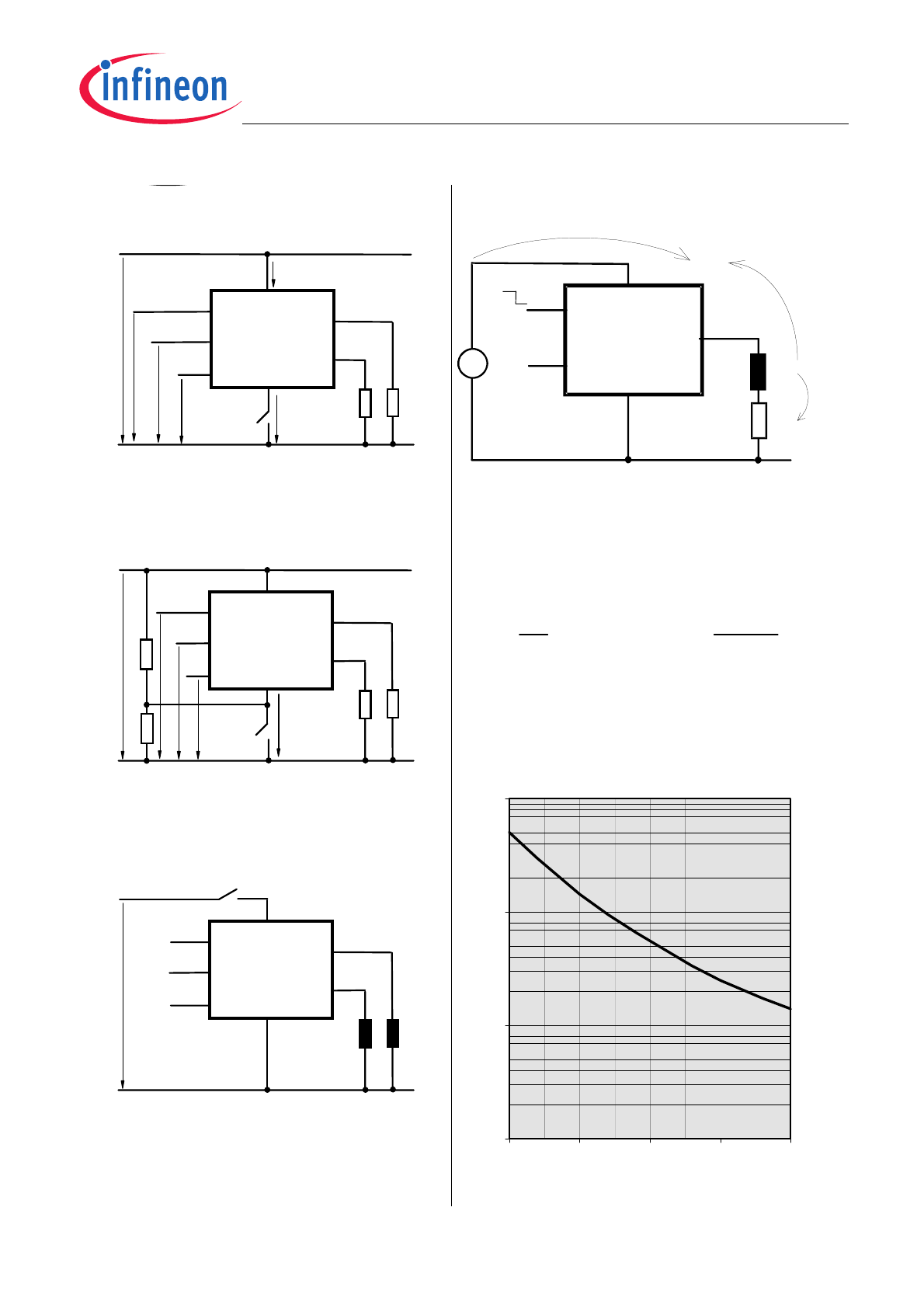
Input circuit (ESD protection),
IN1...4
,1
*1'
,
5
(6'='
,,
,
ESD zener diodes are not to be used as voltage clamp at
DC conditions. Operation in this mode may result in a drift of
the zener voltage (increase of up to 1 V).
Status output,
ST1/2 or ST3/4
67
*1'
(6'
='
9
5
6721
ESD-Zener diode: 6.1 V typ., max 5.0 mA; R
ST(ON)
< 380
Ω
at 1.6 mA, ESD zener diodes are not to be used as voltage
clamp at DC conditions. Operation in this mode may resul
t
in
a drift of the zener voltage (increase of up to 1 V).
Inductive and overvoltage output clamp,
OUT1...4
9EE
287
352)(7
9=
9
21
3RZHU*1'
V
ON
clamped to
V
ON(CL)
= 47 V typ.
Overvoltage protection of logic part
GND1/2 or GND3/4
9EE
,1
67
67
5
*1'
*1'
5
6LJQDO*1'
/RJLF
9=
,1
5,
9=
V
Z1
= 6.1 V typ., V
Z2
= 47 V typ., R
I
= 3.5 k
Ω
typ.
,
R
GND
= 150
Ω
Reverse battery protection
*1'
/RJLF
67
5
,1
67
9
287
/
5
3RZHU*1'
*1'
5
6LJQDO*1'
3RZHU
,QYHUVH
,
5
9EE
'LRGH
R
GND
= 150
Ω,
R
I
= 3.5 k
Ω
typ
,
Temperature protection is not active during inverse current
operation.
Open-load detection,
OUT1...4
OFF-state diagnostic condition:
V
OUT
> 3 V typ.; IN low
2SHQORDG
GHWHFWLRQ
/RJLF
XQLW
9287
6LJQDO*1'
, /2/
2))
Data Sheet
10
Rev 1.3, 2010-03-16
Smart High-Side Power Switch
BTS712N1
GND disconnect
(channel 1/2 or 3/4)
352)(7
9
,1
67
287
*1'
EE
9EE
,EE
,1
287
9,19,1 967
9
*1'
Any kind of load. In case of IN = high is
V
OUT
≈
V
IN
-
V
IN(T+)
.
Due to V
GND
> 0, no V
ST
= low signal available.
GND disconnect with GND pull up
(channel 1/2 or 3/4)
352)(7
9
,1
67
287
*1'
EE
9EE
,1
287
9,1
9,1
967
9*1'
Any kind of load. If V
GND
>
V
IN
-
V
IN(T+)
device stays off
Due to V
GND
> 0, no V
ST
= low signal available.
V
bb
disconnect with energized inductive
load
352)(7
9
,1
67
287
*1'
EE
9EE
,1
287
KLJK
For an inductive load current up to the limit defined by EAS
(max. ratings see page 3 and diagram on page 9) each
switch is protected against loss of Vbb.
Consider at your PCB layout that in the case of Vbb dis-
connection with energized inductive load the whole load
current flows through the GND connection.
Inductive load switch-off energy
dissipation
352)(7
9
,1
67
287
*1'
EE
(
(
(
($6
EE
/
5
(/RDG
5/
/
^
/
=
Energy stored in load inductance:
E
L
=
1/2
·
L
·
I
2
L
While demagnetizing load inductance, the energy
dissipated in PROFET is
E
AS
= E
bb
+ E
L
- E
R
=
V
ON(CL)
·
i
L
(t) dt,
with an approximate solution for RL
>
0
Ω
:
E
AS
=
I
L
·
L
2
·
R
L
(
V
bb
+ |V
OUT(CL)
|)
OQ
(1+
I
L
·
R
L
|V
OUT(CL)
|
)
Maximum allowable load inductance for
a single switch off
(one channel)
5)
/ I,/
Tj,start = 150°C, Vbb = 12 V, RL = 0
Ω
L [mH]
IL [A]