

Data Sheet
Rev. 2.1, 2011-09-01
Automotive Power
BTS5090-2EKA
Smart High-Side Power Switch
Dual Channel, 90m
Ω
PROFET™+ 12V

Data Sheet
2
Rev. 2.1, 2011-09-01
PROFET™+ 12V
BTS5090-2EKA
Table of Contents
1
Overview . . . . . . . . . . . . . . . . . . . . . . . . . . . . . . . . . . . . . . . . . . . . . . . . . . . . . . . . . . . . . . . . . . . . . . . 4
2
Block Diagram . . . . . . . . . . . . . . . . . . . . . . . . . . . . . . . . . . . . . . . . . . . . . . . . . . . . . . . . . . . . . . . . . . . 6
3
Pin Configuration . . . . . . . . . . . . . . . . . . . . . . . . . . . . . . . . . . . . . . . . . . . . . . . . . . . . . . . . . . . . . . . . 7
3.1
Pin Assignment . . . . . . . . . . . . . . . . . . . . . . . . . . . . . . . . . . . . . . . . . . . . . . . . . . . . . . . . . . . . . . . . . . . 7
3.2
Pin Definitions and Functions . . . . . . . . . . . . . . . . . . . . . . . . . . . . . . . . . . . . . . . . . . . . . . . . . . . . . . . . 7
3.3
Voltage and Current Definition . . . . . . . . . . . . . . . . . . . . . . . . . . . . . . . . . . . . . . . . . . . . . . . . . . . . . . . 8
4
General Product Characteristics . . . . . . . . . . . . . . . . . . . . . . . . . . . . . . . . . . . . . . . . . . . . . . . . . . . . 9
4.1
Absolute Maximum Ratings . . . . . . . . . . . . . . . . . . . . . . . . . . . . . . . . . . . . . . . . . . . . . . . . . . . . . . . . . 9
4.2
Functional Range . . . . . . . . . . . . . . . . . . . . . . . . . . . . . . . . . . . . . . . . . . . . . . . . . . . . . . . . . . . . . . . . 11
4.3
Thermal Resistance . . . . . . . . . . . . . . . . . . . . . . . . . . . . . . . . . . . . . . . . . . . . . . . . . . . . . . . . . . . . . . 12
4.3.1
PCB set up . . . . . . . . . . . . . . . . . . . . . . . . . . . . . . . . . . . . . . . . . . . . . . . . . . . . . . . . . . . . . . . . . . . . 12
4.3.2
Thermal Impedance . . . . . . . . . . . . . . . . . . . . . . . . . . . . . . . . . . . . . . . . . . . . . . . . . . . . . . . . . . . . . 13
5
Power Stage . . . . . . . . . . . . . . . . . . . . . . . . . . . . . . . . . . . . . . . . . . . . . . . . . . . . . . . . . . . . . . . . . . . 15
5.1
Output ON-state Resistance . . . . . . . . . . . . . . . . . . . . . . . . . . . . . . . . . . . . . . . . . . . . . . . . . . . . . . . . 15
5.2
Turn ON/OFF Characteristics with Resistive Load . . . . . . . . . . . . . . . . . . . . . . . . . . . . . . . . . . . . . . . 15
5.3
Inductive Load . . . . . . . . . . . . . . . . . . . . . . . . . . . . . . . . . . . . . . . . . . . . . . . . . . . . . . . . . . . . . . . . . . 16
5.3.1
Output Clamping . . . . . . . . . . . . . . . . . . . . . . . . . . . . . . . . . . . . . . . . . . . . . . . . . . . . . . . . . . . . . . . 16
5.3.2
Maximum Load Inductance . . . . . . . . . . . . . . . . . . . . . . . . . . . . . . . . . . . . . . . . . . . . . . . . . . . . . . . 17
5.4
Inverse Current Capability . . . . . . . . . . . . . . . . . . . . . . . . . . . . . . . . . . . . . . . . . . . . . . . . . . . . . . . . . 17
5.5
Electrical Characteristics Power Stage . . . . . . . . . . . . . . . . . . . . . . . . . . . . . . . . . . . . . . . . . . . . . . . . 19
6
Protection Functions . . . . . . . . . . . . . . . . . . . . . . . . . . . . . . . . . . . . . . . . . . . . . . . . . . . . . . . . . . . . 21
6.1
Loss of Ground Protection . . . . . . . . . . . . . . . . . . . . . . . . . . . . . . . . . . . . . . . . . . . . . . . . . . . . . . . . . 21
6.2
Undervoltage Protection . . . . . . . . . . . . . . . . . . . . . . . . . . . . . . . . . . . . . . . . . . . . . . . . . . . . . . . . . . . 21
6.3
Overvoltage Protection . . . . . . . . . . . . . . . . . . . . . . . . . . . . . . . . . . . . . . . . . . . . . . . . . . . . . . . . . . . . 22
6.4
Reverse Polarity Protection . . . . . . . . . . . . . . . . . . . . . . . . . . . . . . . . . . . . . . . . . . . . . . . . . . . . . . . . 23
6.5
Overload Protection . . . . . . . . . . . . . . . . . . . . . . . . . . . . . . . . . . . . . . . . . . . . . . . . . . . . . . . . . . . . . . 23
6.5.1
Current Limitation . . . . . . . . . . . . . . . . . . . . . . . . . . . . . . . . . . . . . . . . . . . . . . . . . . . . . . . . . . . . . . 23
6.5.2
Temperature Limitation in the Power DMOS . . . . . . . . . . . . . . . . . . . . . . . . . . . . . . . . . . . . . . . . . . 24
6.5.3
Short Circuit Appearance with Channel in Parallel . . . . . . . . . . . . . . . . . . . . . . . . . . . . . . . . . . . . . 25
6.6
Electrical Characteristics for the Protection Functions . . . . . . . . . . . . . . . . . . . . . . . . . . . . . . . . . . . . 26
7
Diagnostic Functions . . . . . . . . . . . . . . . . . . . . . . . . . . . . . . . . . . . . . . . . . . . . . . . . . . . . . . . . . . . . 27
7.1
IS Pin . . . . . . . . . . . . . . . . . . . . . . . . . . . . . . . . . . . . . . . . . . . . . . . . . . . . . . . . . . . . . . . . . . . . . . . . . 27
7.2
SENSE Signal in Different Operating Modes . . . . . . . . . . . . . . . . . . . . . . . . . . . . . . . . . . . . . . . . . . . 28
7.3
SENSE Signal in the Nominal Current Range . . . . . . . . . . . . . . . . . . . . . . . . . . . . . . . . . . . . . . . . . . 29
7.3.1
SENSE Signal Variation as a Function of Temperature and Load Current . . . . . . . . . . . . . . . . . . . 29
7.3.2
SENSE Signal Timing . . . . . . . . . . . . . . . . . . . . . . . . . . . . . . . . . . . . . . . . . . . . . . . . . . . . . . . . . . . 30
7.3.3
SENSE Signal in Open Load . . . . . . . . . . . . . . . . . . . . . . . . . . . . . . . . . . . . . . . . . . . . . . . . . . . . . . 31
7.3.3.1
Open Load in ON Diagnostic . . . . . . . . . . . . . . . . . . . . . . . . . . . . . . . . . . . . . . . . . . . . . . . . . . . . 31
7.3.3.2
Open Load in OFF Diagnostic . . . . . . . . . . . . . . . . . . . . . . . . . . . . . . . . . . . . . . . . . . . . . . . . . . . 31
7.3.3.3
Open Load Diagnostic Timing . . . . . . . . . . . . . . . . . . . . . . . . . . . . . . . . . . . . . . . . . . . . . . . . . . . 32
7.3.4
SENSE Signal with OUT in Short Circuit to
V
S
. . . . . . . . . . . . . . . . . . . . . . . . . . . . . . . . . . . . . . . . 33
7.3.5
SENSE Signal in Case of Overload . . . . . . . . . . . . . . . . . . . . . . . . . . . . . . . . . . . . . . . . . . . . . . . . . 33
7.3.6
SENSE Signal in Case of Inverse Current . . . . . . . . . . . . . . . . . . . . . . . . . . . . . . . . . . . . . . . . . . . . 33
7.4
Electrical Characteristics Diagnostic Function . . . . . . . . . . . . . . . . . . . . . . . . . . . . . . . . . . . . . . . . . . 34
8
Input Pins . . . . . . . . . . . . . . . . . . . . . . . . . . . . . . . . . . . . . . . . . . . . . . . . . . . . . . . . . . . . . . . . . . . . . 37
8.1
Input Circuitry . . . . . . . . . . . . . . . . . . . . . . . . . . . . . . . . . . . . . . . . . . . . . . . . . . . . . . . . . . . . . . . . . . . 37
Table of Contents

Data Sheet
3
Rev. 2.1, 2011-09-01
PROFET™+ 12V
BTS5090-2EKA
Table of Contents
8.2
DEN / DSEL Pin . . . . . . . . . . . . . . . . . . . . . . . . . . . . . . . . . . . . . . . . . . . . . . . . . . . . . . . . . . . . . . . . . 37
8.3
Input Pin Voltage . . . . . . . . . . . . . . . . . . . . . . . . . . . . . . . . . . . . . . . . . . . . . . . . . . . . . . . . . . . . . . . . 37
8.4
Electrical Characteristics . . . . . . . . . . . . . . . . . . . . . . . . . . . . . . . . . . . . . . . . . . . . . . . . . . . . . . . . . . 38
9
Characterization Results . . . . . . . . . . . . . . . . . . . . . . . . . . . . . . . . . . . . . . . . . . . . . . . . . . . . . . . . . 39
9.1
General Product Characteristics . . . . . . . . . . . . . . . . . . . . . . . . . . . . . . . . . . . . . . . . . . . . . . . . . . . . . 39
9.1.1
Minimum Functional Supply Voltage . . . . . . . . . . . . . . . . . . . . . . . . . . . . . . . . . . . . . . . . . . . . . . . . 39
9.1.2
Undervoltage Shutdown . . . . . . . . . . . . . . . . . . . . . . . . . . . . . . . . . . . . . . . . . . . . . . . . . . . . . . . . . 39
9.1.3
Current Consumption One Channel active . . . . . . . . . . . . . . . . . . . . . . . . . . . . . . . . . . . . . . . . . . . 40
9.1.4
Current Consumption Two Channels active . . . . . . . . . . . . . . . . . . . . . . . . . . . . . . . . . . . . . . . . . . 40
9.1.5
Standby Current for Whole Device with Load . . . . . . . . . . . . . . . . . . . . . . . . . . . . . . . . . . . . . . . . . 40
9.2
Power Stage . . . . . . . . . . . . . . . . . . . . . . . . . . . . . . . . . . . . . . . . . . . . . . . . . . . . . . . . . . . . . . . . . . . . 41
9.2.1
Output Voltage Drop Limitation at Low Load Current . . . . . . . . . . . . . . . . . . . . . . . . . . . . . . . . . . . 41
9.2.2
Drain to Source Clamp Voltage . . . . . . . . . . . . . . . . . . . . . . . . . . . . . . . . . . . . . . . . . . . . . . . . . . . . 41
9.2.3
Slew Rate at Turn ON . . . . . . . . . . . . . . . . . . . . . . . . . . . . . . . . . . . . . . . . . . . . . . . . . . . . . . . . . . . 42
9.2.4
Slew Rate at Turn OFF . . . . . . . . . . . . . . . . . . . . . . . . . . . . . . . . . . . . . . . . . . . . . . . . . . . . . . . . . . 42
9.2.5
Turn ON . . . . . . . . . . . . . . . . . . . . . . . . . . . . . . . . . . . . . . . . . . . . . . . . . . . . . . . . . . . . . . . . . . . . . . 42
9.2.6
Turn OFF . . . . . . . . . . . . . . . . . . . . . . . . . . . . . . . . . . . . . . . . . . . . . . . . . . . . . . . . . . . . . . . . . . . . . 43
9.2.7
Turn ON / OFF matching . . . . . . . . . . . . . . . . . . . . . . . . . . . . . . . . . . . . . . . . . . . . . . . . . . . . . . . . . 43
9.2.8
Switch ON Energy . . . . . . . . . . . . . . . . . . . . . . . . . . . . . . . . . . . . . . . . . . . . . . . . . . . . . . . . . . . . . . 44
9.2.9
Switch OFF Energy . . . . . . . . . . . . . . . . . . . . . . . . . . . . . . . . . . . . . . . . . . . . . . . . . . . . . . . . . . . . . 44
9.3
Protection Functions . . . . . . . . . . . . . . . . . . . . . . . . . . . . . . . . . . . . . . . . . . . . . . . . . . . . . . . . . . . . . . 45
9.3.1
Overload Condition in the Low Voltage Area . . . . . . . . . . . . . . . . . . . . . . . . . . . . . . . . . . . . . . . . . . 45
9.3.2
Overload Condition in the High Voltage Area . . . . . . . . . . . . . . . . . . . . . . . . . . . . . . . . . . . . . . . . . 45
9.4
Diagnostic Mechanism . . . . . . . . . . . . . . . . . . . . . . . . . . . . . . . . . . . . . . . . . . . . . . . . . . . . . . . . . . . . 46
9.4.1
Current Sense at no Load . . . . . . . . . . . . . . . . . . . . . . . . . . . . . . . . . . . . . . . . . . . . . . . . . . . . . . . . 46
9.4.2
Open Load Detection Threshold in ON State . . . . . . . . . . . . . . . . . . . . . . . . . . . . . . . . . . . . . . . . . 46
9.4.3
Sense Signal Maximum Voltage . . . . . . . . . . . . . . . . . . . . . . . . . . . . . . . . . . . . . . . . . . . . . . . . . . . 47
9.4.4
Sense Signal maximum Current . . . . . . . . . . . . . . . . . . . . . . . . . . . . . . . . . . . . . . . . . . . . . . . . . . . 47
9.5
Input Pins . . . . . . . . . . . . . . . . . . . . . . . . . . . . . . . . . . . . . . . . . . . . . . . . . . . . . . . . . . . . . . . . . . . . . . 48
9.5.1
Input Voltage Threshold ON to OFF . . . . . . . . . . . . . . . . . . . . . . . . . . . . . . . . . . . . . . . . . . . . . . . . 48
9.5.2
Input Voltage Threshold OFF to ON . . . . . . . . . . . . . . . . . . . . . . . . . . . . . . . . . . . . . . . . . . . . . . . . 48
9.5.3
Input Voltage Hysteresis . . . . . . . . . . . . . . . . . . . . . . . . . . . . . . . . . . . . . . . . . . . . . . . . . . . . . . . . . 49
9.5.4
Input Current High Level . . . . . . . . . . . . . . . . . . . . . . . . . . . . . . . . . . . . . . . . . . . . . . . . . . . . . . . . . 49
10
Application Information . . . . . . . . . . . . . . . . . . . . . . . . . . . . . . . . . . . . . . . . . . . . . . . . . . . . . . . . . . 50
10.1
Further Application Information . . . . . . . . . . . . . . . . . . . . . . . . . . . . . . . . . . . . . . . . . . . . . . . . . . . . . . 51
11
Package Outlines . . . . . . . . . . . . . . . . . . . . . . . . . . . . . . . . . . . . . . . . . . . . . . . . . . . . . . . . . . . . . . . 52
12
Revision History . . . . . . . . . . . . . . . . . . . . . . . . . . . . . . . . . . . . . . . . . . . . . . . . . . . . . . . . . . . . . . . . 53
PG-DSO-14-40 EP
Type
Package
Marking
BTS5090-2EKA
PG-DSO-14-40 EP
BTS5090-2EKA
Data Sheet
4
Rev. 2.1, 2011-09-01
PROFET™+ 12V
Smart High-Side Power Switch
BTS5090-2EKA
1
Overview
Application
•
Suitable for resistive, inductive and capacitive loads
•
Replaces electromechanical relays, fuses and discrete circuits
•
Most suitable for loads with high inrush current, such as lamps
Basic Features
•
Two channel device
•
Very low stand-by current
•
3.3 V and 5 V compatible logic inputs
•
Electrostatic discharge protection (ESD)
•
Optimized electromagnetic compatibility
•
Logic ground independent from load ground
•
Very low power DMOS leakage current in OFF state
•
Green product (RoHS compliant)
•
AEC qualified
Description
The BTS5090-2EKA is a 90 m
Ω dual channel Smart High-Side Power Switch, embedded in a PG-DSO-14-40 EP,
Exposed Pad package, providing protective functions and diagnosis. The power transistor is built by an N-channel
vertical power MOSFET with charge pump. The device is integrated in Smart6 technology. It is specially designed
to drive lamps up to 1 * P21W, as well as LEDs in the harsh automotive environment.
Table 1
Product Summary
Parameter
Symbol
Value
Operating voltage range
V
S(OP)
5 V ... 28 V
Maximum supply voltage
V
S(LD)
41 V
Maximum ON state resistance at
T
J
= 150
°C per channel
R
DS(ON)
180 m
Ω
Nominal load current (one channel active)
I
L(NOM)1
3.5 A
Nominal load current (both channels active)
I
L(NOM)2
2.5 A
Typical current sense ratio
k
ILIS
1500
Minimum current limitation
I
L5(SC)
20 A
Maximum standby current with load at
T
J
= 25 °C
I
S(OFF)
500 nA

Data Sheet
5
Rev. 2.1, 2011-09-01
PROFET™+ 12V
BTS5090-2EKA
Overview
Diagnostic Functions
•
Proportional load current sense for both channels multiplexed
•
Open load in ON and OFF
•
Short circuit to battery and ground
•
Overtemperature
•
Stable diagnostic signal during short circuit
•
Enhanced
k
ILIS
dependency with temperature and load current
Protection Functions
•
Stable behavior during undervoltage
•
Reverse polarity protection with external components
•
Secure load turn-off during logic ground disconnect with external components
•
Overtemperature protection with restart
•
Overvoltage protection with external components
•
Voltage dependent current limitation
•
Enhanced short circuit operation
BTS5090-2EKA
Block Diagram
Data Sheet
6
Rev. 2.1, 2011-09-01
PROFET™+ 12V
2
Block Diagram
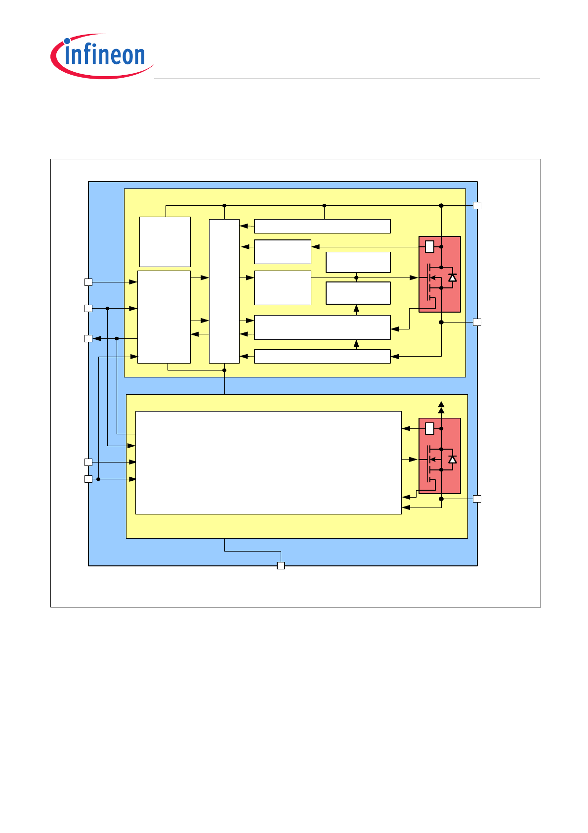
Figure 1
Block Diagram for the BTS5090-2EKA
Block diagram DxS.vsd
Channel 0
V
S
OUT 0
IN0
T
driver
logic
gate control
&
charge pump
load current sense and
open load detection
over
temperature
clamp for
inductive load
over current
switch limit
forward voltage drop detection
voltage sensor
GND
ESD
protection
IS
DEN
Channel 1
DSEL
IN1
Control and protection circuit equivalent to channel 0
T
V
S
OUT 1
internal
power
supply
Data Sheet
7
Rev. 2.1, 2011-09-01
PROFET™+ 12V
BTS5090-2EKA
Pin Configuration
3
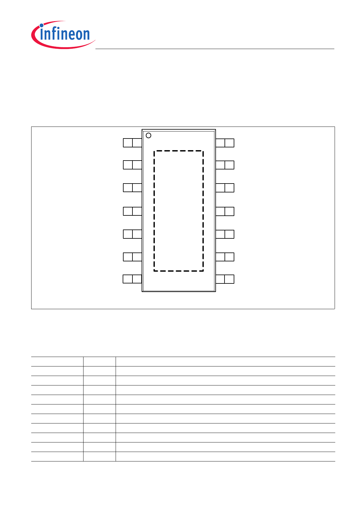
Pin Configuration
3.1
Pin Assignment
Figure 2
Pin Configuration
3.2
Pin Definitions and Functions
Pin
Symbol
Function
1
GND
GrouND; Ground connection
2
IN0
INput channel 0; Input signal for channel 0 activation
3
DEN
Diagnostic ENable; Digital signal to enable/disable the diagnosis of the device
4
IS
Sense; Sense current of the selected channel
5
DSEL
Diagnostic SELection; Digital signal to select the channel to be diagnosed
6
IN1
INput channel 1; Input signal for channel 1 activation
7, 11
NC
Not Connected; No internal connection to the chip
8, 9, 10
OUT1
OUTput 1; Protected high side power output channel 1
1)
1) All output pins of a given channel must be connected together on the PCB. All pins of an output are internally connected
together. PCB traces have to be designed to withstand the maximum current which can flow.
12, 13, 14
OUT0
OUTput 0; Protected high side power output channel 0
1)
Cooling Tab
V
S
Voltage Supply; Battery voltage
Pinout dual SO14.vsd
OUT0
OUT0
OUT0
NC
OUT1
OUT1
OUT1
GND
IN0
DEN
IS
DSEL
IN1
NC
14
13
12
11
10
9
8
1
2
3
4
5
6
7
BTS5090-2EKA
Pin Configuration
Data Sheet
8
Rev. 2.1, 2011-09-01
PROFET™+ 12V
3.3
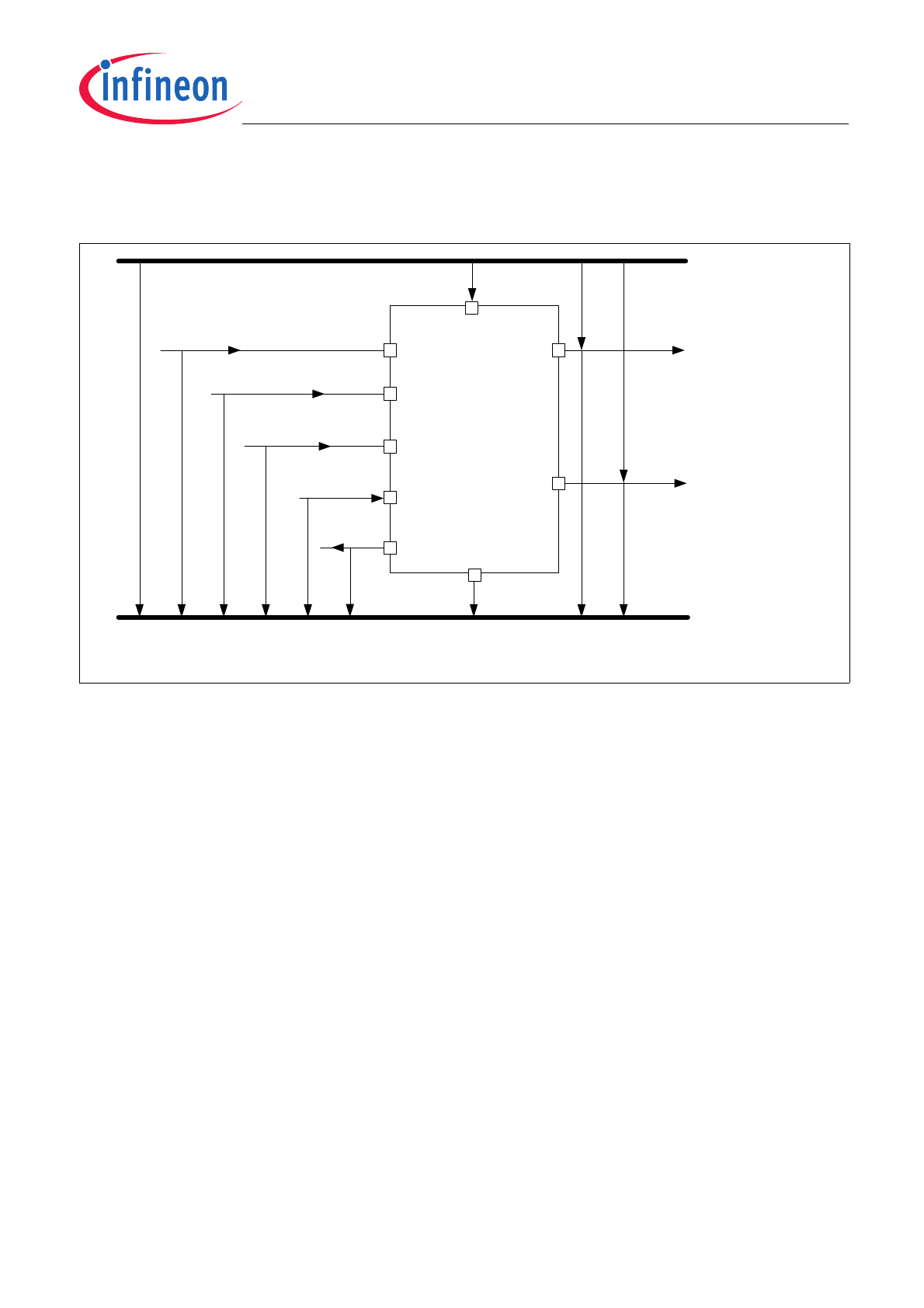
Voltage and Current Definition
Figure 3
shows all terms used in this data sheet, with associated convention for positive values.
Figure 3
Voltage and Current Definition
V
S
IN0
IN1
DEN
DSEL
IS
GND
OUT0
OUT1
I
IN0
I
IN1
I
DEN
I
DSEL
I
IS
V
S
V
IN0
V
IN1
V
DEN
V
DSEL
V
IS
I
S
I
GND
V
DS0
V
DS1
V
OUT0
V
OUT1
I
OUT1
I
OUT0
voltage and current convention.vsd

Data Sheet
9
Rev. 2.1, 2011-09-01
PROFET™+ 12V
BTS5090-2EKA
General Product Characteristics
4
General Product Characteristics
4.1
Absolute Maximum Ratings
Table 2
Absolute Maximum Ratings
1)
T
J
= -40°C to +150°C; (unless otherwise specified)
Parameter
Symbol
Values
Unit
Note /
Test Condition
Number
Min.
Typ.
Max.
Supply Voltages
Supply voltage
V
S
-0.3
–
28
V
–
P_4.1.1
Reverse polarity voltage
-
V
S(REV)
0
–
16
V
t
< 2 min
T
A
= 25
°C
R
L
≥ 6 Ω
R
GND
= 150
Ω
P_4.1.2
Supply voltage for short
circuit protection
V
BAT(SC)
0
–
24
V
2)
R
ECU
= 20 m
Ω
R
Cable
= 16 m
Ω/m
L
Cable
= 1
μH/m,
l
= 0 or 5 m
See
Chapter 6
and
Figure 53
P_4.1.3
Supply voltage for Load dump
protection
V
S(LD)
– –
41 V
3)
R
I
= 2
Ω
R
L
= 6
Ω
P_4.1.12
Short Circuit Capability
Permanent short circuit
IN pin toggles
n
RSC1
– –
100
k
cycle
4)
t
ON
= 300ms
P_4.1.4
Input Pins
Voltage at INPUT pins
V
IN
-0.3
–
–
6
7
V
–
t
< 2 min
P_4.1.13
Current through INPUT pins
I
IN
-2
–
2
mA
–
P_4.1.14
Voltage at DEN pin
V
DEN
-0.3
–
–
6
7
V
–
t
< 2 min
P_4.1.15
Current through DEN pin
I
DEN
-2
–
2
mA
–
P_4.1.16
Voltage at DSEL pin
V
DSEL
-0.3
–
–
6
7
V
–
t
< 2 min
P_4.1.17
Current through DSEL pin
I
DSEL
-2
–
2
mA
–
P_4.1.18
Sense Pin
Voltage at IS pin
V
IS
-0.3
–
V
S
V
–
P_4.1.19
Current through IS pin
I
IS
-25
–
50
mA
–
P_4.1.20
Power Stage
Load current
|
I
L
|
–
–
I
L(LIM)
A
–
P_4.1.21
Power dissipation (DC)
P
TOT
–
–
1.9
W
T
A
= 85
°C
T
J
< 150
°C
P_4.1.22

BTS5090-2EKA
General Product Characteristics
Data Sheet
10
Rev. 2.1, 2011-09-01
PROFET™+ 12V
Notes
1. Stresses above the ones listed here may cause permanent damage to the device. Exposure to absolute
maximum rating conditions for extended periods may affect device reliability.
2. Integrated protection functions are designed to prevent IC destruction under fault conditions described in the
data sheet. Fault conditions are considered as “outside” normal operating range. Protection functions are not
designed for continuous repetitive operation.
Maximum energy dissipation
Single pulse (one channel)
E
AS
–
–
42
mJ
I
L(0)
= 3 A
T
J(0)
= 150
°C
V
S
= 13.5 V
P_4.1.23
Voltage at power transistor
V
DS
–
–
41
V
–
P_4.1.26
Currents
Current through ground pin
I
GND
-10
-150
–
10
20
mA
–
t
< 2 min
P_4.1.27
Temperatures
Junction temperature
T
J
-40
–
150
°C
–
P_4.1.28
Storage temperature
T
STG
-55
–
150
°C
–
P_4.1.30
ESD Susceptibility
ESD susceptibility (all pins)
V
ESD
-2
–
2
kV
5)
HBM
P_4.1.31
ESD susceptibility OUT Pin
vs. GND and
V
S
connected
V
ESD
-4
–
4
kV
5)
HBM
P_4.1.32
ESD susceptibility
V
ESD
-500
–
500
V
6)
CDM
P_4.1.33
ESD susceptibility pin
(corner pins)
V
ESD
-750
–
750
V
6)
CDM
P_4.1.34
1) Not subject to production test. Specified by design.
2) Hardware set-up in accordance to AEC Q100-012 and AEC Q101-006.
3)
V
S(LD)
is setup without the DUT connected to the generator per ISO 7637-1.
4) EOL tests according to AECQ100-012. Threshold limit for short circuit failures: 100 ppm. Please refer to the legal disclaimer
for short-circuit capability on Page 54 of this document.
5) ESD susceptibility HBM according to EIA/JESD 22-A 114B.
6) “CDM” EIA/JESD22-C101 or ESDA STM5.3.1
Table 2
Absolute Maximum Ratings (cont’d)
1)
T
J
= -40°C to +150°C; (unless otherwise specified)
Parameter
Symbol
Values
Unit
Note /
Test Condition
Number
Min.
Typ.
Max.
Data Sheet
Rev. 2.1, 2011-09-01
Automotive Power
BTS5090-2EKA
Smart High-Side Power Switch
Dual Channel, 90m
Ω
PROFET™+ 12V
Data Sheet
2
Rev. 2.1, 2011-09-01
PROFET™+ 12V
BTS5090-2EKA
Table of Contents
1
Overview . . . . . . . . . . . . . . . . . . . . . . . . . . . . . . . . . . . . . . . . . . . . . . . . . . . . . . . . . . . . . . . . . . . . . . . 4
2
Block Diagram . . . . . . . . . . . . . . . . . . . . . . . . . . . . . . . . . . . . . . . . . . . . . . . . . . . . . . . . . . . . . . . . . . . 6
3
Pin Configuration . . . . . . . . . . . . . . . . . . . . . . . . . . . . . . . . . . . . . . . . . . . . . . . . . . . . . . . . . . . . . . . . 7
3.1
Pin Assignment . . . . . . . . . . . . . . . . . . . . . . . . . . . . . . . . . . . . . . . . . . . . . . . . . . . . . . . . . . . . . . . . . . . 7
3.2
Pin Definitions and Functions . . . . . . . . . . . . . . . . . . . . . . . . . . . . . . . . . . . . . . . . . . . . . . . . . . . . . . . . 7
3.3
Voltage and Current Definition . . . . . . . . . . . . . . . . . . . . . . . . . . . . . . . . . . . . . . . . . . . . . . . . . . . . . . . 8
4
General Product Characteristics . . . . . . . . . . . . . . . . . . . . . . . . . . . . . . . . . . . . . . . . . . . . . . . . . . . . 9
4.1
Absolute Maximum Ratings . . . . . . . . . . . . . . . . . . . . . . . . . . . . . . . . . . . . . . . . . . . . . . . . . . . . . . . . . 9
4.2
Functional Range . . . . . . . . . . . . . . . . . . . . . . . . . . . . . . . . . . . . . . . . . . . . . . . . . . . . . . . . . . . . . . . . 11
4.3
Thermal Resistance . . . . . . . . . . . . . . . . . . . . . . . . . . . . . . . . . . . . . . . . . . . . . . . . . . . . . . . . . . . . . . 12
4.3.1
PCB set up . . . . . . . . . . . . . . . . . . . . . . . . . . . . . . . . . . . . . . . . . . . . . . . . . . . . . . . . . . . . . . . . . . . . 12
4.3.2
Thermal Impedance . . . . . . . . . . . . . . . . . . . . . . . . . . . . . . . . . . . . . . . . . . . . . . . . . . . . . . . . . . . . . 13
5
Power Stage . . . . . . . . . . . . . . . . . . . . . . . . . . . . . . . . . . . . . . . . . . . . . . . . . . . . . . . . . . . . . . . . . . . 15
5.1
Output ON-state Resistance . . . . . . . . . . . . . . . . . . . . . . . . . . . . . . . . . . . . . . . . . . . . . . . . . . . . . . . . 15
5.2
Turn ON/OFF Characteristics with Resistive Load . . . . . . . . . . . . . . . . . . . . . . . . . . . . . . . . . . . . . . . 15
5.3
Inductive Load . . . . . . . . . . . . . . . . . . . . . . . . . . . . . . . . . . . . . . . . . . . . . . . . . . . . . . . . . . . . . . . . . . 16
5.3.1
Output Clamping . . . . . . . . . . . . . . . . . . . . . . . . . . . . . . . . . . . . . . . . . . . . . . . . . . . . . . . . . . . . . . . 16
5.3.2
Maximum Load Inductance . . . . . . . . . . . . . . . . . . . . . . . . . . . . . . . . . . . . . . . . . . . . . . . . . . . . . . . 17
5.4
Inverse Current Capability . . . . . . . . . . . . . . . . . . . . . . . . . . . . . . . . . . . . . . . . . . . . . . . . . . . . . . . . . 17
5.5
Electrical Characteristics Power Stage . . . . . . . . . . . . . . . . . . . . . . . . . . . . . . . . . . . . . . . . . . . . . . . . 19
6
Protection Functions . . . . . . . . . . . . . . . . . . . . . . . . . . . . . . . . . . . . . . . . . . . . . . . . . . . . . . . . . . . . 21
6.1
Loss of Ground Protection . . . . . . . . . . . . . . . . . . . . . . . . . . . . . . . . . . . . . . . . . . . . . . . . . . . . . . . . . 21
6.2
Undervoltage Protection . . . . . . . . . . . . . . . . . . . . . . . . . . . . . . . . . . . . . . . . . . . . . . . . . . . . . . . . . . . 21
6.3
Overvoltage Protection . . . . . . . . . . . . . . . . . . . . . . . . . . . . . . . . . . . . . . . . . . . . . . . . . . . . . . . . . . . . 22
6.4
Reverse Polarity Protection . . . . . . . . . . . . . . . . . . . . . . . . . . . . . . . . . . . . . . . . . . . . . . . . . . . . . . . . 23
6.5
Overload Protection . . . . . . . . . . . . . . . . . . . . . . . . . . . . . . . . . . . . . . . . . . . . . . . . . . . . . . . . . . . . . . 23
6.5.1
Current Limitation . . . . . . . . . . . . . . . . . . . . . . . . . . . . . . . . . . . . . . . . . . . . . . . . . . . . . . . . . . . . . . 23
6.5.2
Temperature Limitation in the Power DMOS . . . . . . . . . . . . . . . . . . . . . . . . . . . . . . . . . . . . . . . . . . 24
6.5.3
Short Circuit Appearance with Channel in Parallel . . . . . . . . . . . . . . . . . . . . . . . . . . . . . . . . . . . . . 25
6.6
Electrical Characteristics for the Protection Functions . . . . . . . . . . . . . . . . . . . . . . . . . . . . . . . . . . . . 26
7
Diagnostic Functions . . . . . . . . . . . . . . . . . . . . . . . . . . . . . . . . . . . . . . . . . . . . . . . . . . . . . . . . . . . . 27
7.1
IS Pin . . . . . . . . . . . . . . . . . . . . . . . . . . . . . . . . . . . . . . . . . . . . . . . . . . . . . . . . . . . . . . . . . . . . . . . . . 27
7.2
SENSE Signal in Different Operating Modes . . . . . . . . . . . . . . . . . . . . . . . . . . . . . . . . . . . . . . . . . . . 28
7.3
SENSE Signal in the Nominal Current Range . . . . . . . . . . . . . . . . . . . . . . . . . . . . . . . . . . . . . . . . . . 29
7.3.1
SENSE Signal Variation as a Function of Temperature and Load Current . . . . . . . . . . . . . . . . . . . 29
7.3.2
SENSE Signal Timing . . . . . . . . . . . . . . . . . . . . . . . . . . . . . . . . . . . . . . . . . . . . . . . . . . . . . . . . . . . 30
7.3.3
SENSE Signal in Open Load . . . . . . . . . . . . . . . . . . . . . . . . . . . . . . . . . . . . . . . . . . . . . . . . . . . . . . 31
7.3.3.1
Open Load in ON Diagnostic . . . . . . . . . . . . . . . . . . . . . . . . . . . . . . . . . . . . . . . . . . . . . . . . . . . . 31
7.3.3.2
Open Load in OFF Diagnostic . . . . . . . . . . . . . . . . . . . . . . . . . . . . . . . . . . . . . . . . . . . . . . . . . . . 31
7.3.3.3
Open Load Diagnostic Timing . . . . . . . . . . . . . . . . . . . . . . . . . . . . . . . . . . . . . . . . . . . . . . . . . . . 32
7.3.4
SENSE Signal with OUT in Short Circuit to
V
S
. . . . . . . . . . . . . . . . . . . . . . . . . . . . . . . . . . . . . . . . 33
7.3.5
SENSE Signal in Case of Overload . . . . . . . . . . . . . . . . . . . . . . . . . . . . . . . . . . . . . . . . . . . . . . . . . 33
7.3.6
SENSE Signal in Case of Inverse Current . . . . . . . . . . . . . . . . . . . . . . . . . . . . . . . . . . . . . . . . . . . . 33
7.4
Electrical Characteristics Diagnostic Function . . . . . . . . . . . . . . . . . . . . . . . . . . . . . . . . . . . . . . . . . . 34
8
Input Pins . . . . . . . . . . . . . . . . . . . . . . . . . . . . . . . . . . . . . . . . . . . . . . . . . . . . . . . . . . . . . . . . . . . . . 37
8.1
Input Circuitry . . . . . . . . . . . . . . . . . . . . . . . . . . . . . . . . . . . . . . . . . . . . . . . . . . . . . . . . . . . . . . . . . . . 37
Table of Contents
Data Sheet
3
Rev. 2.1, 2011-09-01
PROFET™+ 12V
BTS5090-2EKA
Table of Contents
8.2
DEN / DSEL Pin . . . . . . . . . . . . . . . . . . . . . . . . . . . . . . . . . . . . . . . . . . . . . . . . . . . . . . . . . . . . . . . . . 37
8.3
Input Pin Voltage . . . . . . . . . . . . . . . . . . . . . . . . . . . . . . . . . . . . . . . . . . . . . . . . . . . . . . . . . . . . . . . . 37
8.4
Electrical Characteristics . . . . . . . . . . . . . . . . . . . . . . . . . . . . . . . . . . . . . . . . . . . . . . . . . . . . . . . . . . 38
9
Characterization Results . . . . . . . . . . . . . . . . . . . . . . . . . . . . . . . . . . . . . . . . . . . . . . . . . . . . . . . . . 39
9.1
General Product Characteristics . . . . . . . . . . . . . . . . . . . . . . . . . . . . . . . . . . . . . . . . . . . . . . . . . . . . . 39
9.1.1
Minimum Functional Supply Voltage . . . . . . . . . . . . . . . . . . . . . . . . . . . . . . . . . . . . . . . . . . . . . . . . 39
9.1.2
Undervoltage Shutdown . . . . . . . . . . . . . . . . . . . . . . . . . . . . . . . . . . . . . . . . . . . . . . . . . . . . . . . . . 39
9.1.3
Current Consumption One Channel active . . . . . . . . . . . . . . . . . . . . . . . . . . . . . . . . . . . . . . . . . . . 40
9.1.4
Current Consumption Two Channels active . . . . . . . . . . . . . . . . . . . . . . . . . . . . . . . . . . . . . . . . . . 40
9.1.5
Standby Current for Whole Device with Load . . . . . . . . . . . . . . . . . . . . . . . . . . . . . . . . . . . . . . . . . 40
9.2
Power Stage . . . . . . . . . . . . . . . . . . . . . . . . . . . . . . . . . . . . . . . . . . . . . . . . . . . . . . . . . . . . . . . . . . . . 41
9.2.1
Output Voltage Drop Limitation at Low Load Current . . . . . . . . . . . . . . . . . . . . . . . . . . . . . . . . . . . 41
9.2.2
Drain to Source Clamp Voltage . . . . . . . . . . . . . . . . . . . . . . . . . . . . . . . . . . . . . . . . . . . . . . . . . . . . 41
9.2.3
Slew Rate at Turn ON . . . . . . . . . . . . . . . . . . . . . . . . . . . . . . . . . . . . . . . . . . . . . . . . . . . . . . . . . . . 42
9.2.4
Slew Rate at Turn OFF . . . . . . . . . . . . . . . . . . . . . . . . . . . . . . . . . . . . . . . . . . . . . . . . . . . . . . . . . . 42
9.2.5
Turn ON . . . . . . . . . . . . . . . . . . . . . . . . . . . . . . . . . . . . . . . . . . . . . . . . . . . . . . . . . . . . . . . . . . . . . . 42
9.2.6
Turn OFF . . . . . . . . . . . . . . . . . . . . . . . . . . . . . . . . . . . . . . . . . . . . . . . . . . . . . . . . . . . . . . . . . . . . . 43
9.2.7
Turn ON / OFF matching . . . . . . . . . . . . . . . . . . . . . . . . . . . . . . . . . . . . . . . . . . . . . . . . . . . . . . . . . 43
9.2.8
Switch ON Energy . . . . . . . . . . . . . . . . . . . . . . . . . . . . . . . . . . . . . . . . . . . . . . . . . . . . . . . . . . . . . . 44
9.2.9
Switch OFF Energy . . . . . . . . . . . . . . . . . . . . . . . . . . . . . . . . . . . . . . . . . . . . . . . . . . . . . . . . . . . . . 44
9.3
Protection Functions . . . . . . . . . . . . . . . . . . . . . . . . . . . . . . . . . . . . . . . . . . . . . . . . . . . . . . . . . . . . . . 45
9.3.1
Overload Condition in the Low Voltage Area . . . . . . . . . . . . . . . . . . . . . . . . . . . . . . . . . . . . . . . . . . 45
9.3.2
Overload Condition in the High Voltage Area . . . . . . . . . . . . . . . . . . . . . . . . . . . . . . . . . . . . . . . . . 45
9.4
Diagnostic Mechanism . . . . . . . . . . . . . . . . . . . . . . . . . . . . . . . . . . . . . . . . . . . . . . . . . . . . . . . . . . . . 46
9.4.1
Current Sense at no Load . . . . . . . . . . . . . . . . . . . . . . . . . . . . . . . . . . . . . . . . . . . . . . . . . . . . . . . . 46
9.4.2
Open Load Detection Threshold in ON State . . . . . . . . . . . . . . . . . . . . . . . . . . . . . . . . . . . . . . . . . 46
9.4.3
Sense Signal Maximum Voltage . . . . . . . . . . . . . . . . . . . . . . . . . . . . . . . . . . . . . . . . . . . . . . . . . . . 47
9.4.4
Sense Signal maximum Current . . . . . . . . . . . . . . . . . . . . . . . . . . . . . . . . . . . . . . . . . . . . . . . . . . . 47
9.5
Input Pins . . . . . . . . . . . . . . . . . . . . . . . . . . . . . . . . . . . . . . . . . . . . . . . . . . . . . . . . . . . . . . . . . . . . . . 48
9.5.1
Input Voltage Threshold ON to OFF . . . . . . . . . . . . . . . . . . . . . . . . . . . . . . . . . . . . . . . . . . . . . . . . 48
9.5.2
Input Voltage Threshold OFF to ON . . . . . . . . . . . . . . . . . . . . . . . . . . . . . . . . . . . . . . . . . . . . . . . . 48
9.5.3
Input Voltage Hysteresis . . . . . . . . . . . . . . . . . . . . . . . . . . . . . . . . . . . . . . . . . . . . . . . . . . . . . . . . . 49
9.5.4
Input Current High Level . . . . . . . . . . . . . . . . . . . . . . . . . . . . . . . . . . . . . . . . . . . . . . . . . . . . . . . . . 49
10
Application Information . . . . . . . . . . . . . . . . . . . . . . . . . . . . . . . . . . . . . . . . . . . . . . . . . . . . . . . . . . 50
10.1
Further Application Information . . . . . . . . . . . . . . . . . . . . . . . . . . . . . . . . . . . . . . . . . . . . . . . . . . . . . . 51
11
Package Outlines . . . . . . . . . . . . . . . . . . . . . . . . . . . . . . . . . . . . . . . . . . . . . . . . . . . . . . . . . . . . . . . 52
12
Revision History . . . . . . . . . . . . . . . . . . . . . . . . . . . . . . . . . . . . . . . . . . . . . . . . . . . . . . . . . . . . . . . . 53
PG-DSO-14-40 EP
Type
Package
Marking
BTS5090-2EKA
PG-DSO-14-40 EP
BTS5090-2EKA
Data Sheet
4
Rev. 2.1, 2011-09-01
PROFET™+ 12V
Smart High-Side Power Switch
BTS5090-2EKA
1
Overview
Application
•
Suitable for resistive, inductive and capacitive loads
•
Replaces electromechanical relays, fuses and discrete circuits
•
Most suitable for loads with high inrush current, such as lamps
Basic Features
•
Two channel device
•
Very low stand-by current
•
3.3 V and 5 V compatible logic inputs
•
Electrostatic discharge protection (ESD)
•
Optimized electromagnetic compatibility
•
Logic ground independent from load ground
•
Very low power DMOS leakage current in OFF state
•
Green product (RoHS compliant)
•
AEC qualified
Description
The BTS5090-2EKA is a 90 m
Ω dual channel Smart High-Side Power Switch, embedded in a PG-DSO-14-40 EP,
Exposed Pad package, providing protective functions and diagnosis. The power transistor is built by an N-channel
vertical power MOSFET with charge pump. The device is integrated in Smart6 technology. It is specially designed
to drive lamps up to 1 * P21W, as well as LEDs in the harsh automotive environment.
Table 1
Product Summary
Parameter
Symbol
Value
Operating voltage range
V
S(OP)
5 V ... 28 V
Maximum supply voltage
V
S(LD)
41 V
Maximum ON state resistance at
T
J
= 150
°C per channel
R
DS(ON)
180 m
Ω
Nominal load current (one channel active)
I
L(NOM)1
3.5 A
Nominal load current (both channels active)
I
L(NOM)2
2.5 A
Typical current sense ratio
k
ILIS
1500
Minimum current limitation
I
L5(SC)
20 A
Maximum standby current with load at
T
J
= 25 °C
I
S(OFF)
500 nA
Data Sheet
5
Rev. 2.1, 2011-09-01
PROFET™+ 12V
BTS5090-2EKA
Overview
Diagnostic Functions
•
Proportional load current sense for both channels multiplexed
•
Open load in ON and OFF
•
Short circuit to battery and ground
•
Overtemperature
•
Stable diagnostic signal during short circuit
•
Enhanced
k
ILIS
dependency with temperature and load current
Protection Functions
•
Stable behavior during undervoltage
•
Reverse polarity protection with external components
•
Secure load turn-off during logic ground disconnect with external components
•
Overtemperature protection with restart
•
Overvoltage protection with external components
•
Voltage dependent current limitation
•
Enhanced short circuit operation
BTS5090-2EKA
Block Diagram
Data Sheet
6
Rev. 2.1, 2011-09-01
PROFET™+ 12V
2
Block Diagram
Figure 1
Block Diagram for the BTS5090-2EKA
Block diagram DxS.vsd
Channel 0
V
S
OUT 0
IN0
T
driver
logic
gate control
&
charge pump
load current sense and
open load detection
over
temperature
clamp for
inductive load
over current
switch limit
forward voltage drop detection
voltage sensor
GND
ESD
protection
IS
DEN
Channel 1
DSEL
IN1
Control and protection circuit equivalent to channel 0
T
V
S
OUT 1
internal
power
supply
Data Sheet
7
Rev. 2.1, 2011-09-01
PROFET™+ 12V
BTS5090-2EKA
Pin Configuration
3
Pin Configuration
3.1
Pin Assignment
Figure 2
Pin Configuration
3.2
Pin Definitions and Functions
Pin
Symbol
Function
1
GND
GrouND; Ground connection
2
IN0
INput channel 0; Input signal for channel 0 activation
3
DEN
Diagnostic ENable; Digital signal to enable/disable the diagnosis of the device
4
IS
Sense; Sense current of the selected channel
5
DSEL
Diagnostic SELection; Digital signal to select the channel to be diagnosed
6
IN1
INput channel 1; Input signal for channel 1 activation
7, 11
NC
Not Connected; No internal connection to the chip
8, 9, 10
OUT1
OUTput 1; Protected high side power output channel 1
1)
1) All output pins of a given channel must be connected together on the PCB. All pins of an output are internally connected
together. PCB traces have to be designed to withstand the maximum current which can flow.
12, 13, 14
OUT0
OUTput 0; Protected high side power output channel 0
1)
Cooling Tab
V
S
Voltage Supply; Battery voltage
Pinout dual SO14.vsd
OUT0
OUT0
OUT0
NC
OUT1
OUT1
OUT1
GND
IN0
DEN
IS
DSEL
IN1
NC
14
13
12
11
10
9
8
1
2
3
4
5
6
7
BTS5090-2EKA
Pin Configuration
Data Sheet
8
Rev. 2.1, 2011-09-01
PROFET™+ 12V
3.3
Voltage and Current Definition
Figure 3
shows all terms used in this data sheet, with associated convention for positive values.
Figure 3
Voltage and Current Definition
V
S
IN0
IN1
DEN
DSEL
IS
GND
OUT0
OUT1
I
IN0
I
IN1
I
DEN
I
DSEL
I
IS
V
S
V
IN0
V
IN1
V
DEN
V
DSEL
V
IS
I
S
I
GND
V
DS0
V
DS1
V
OUT0
V
OUT1
I
OUT1
I
OUT0
voltage and current convention.vsd
Data Sheet
9
Rev. 2.1, 2011-09-01
PROFET™+ 12V
BTS5090-2EKA
General Product Characteristics
4
General Product Characteristics
4.1
Absolute Maximum Ratings
Table 2
Absolute Maximum Ratings
1)
T
J
= -40°C to +150°C; (unless otherwise specified)
Parameter
Symbol
Values
Unit
Note /
Test Condition
Number
Min.
Typ.
Max.
Supply Voltages
Supply voltage
V
S
-0.3
–
28
V
–
P_4.1.1
Reverse polarity voltage
-
V
S(REV)
0
–
16
V
t
< 2 min
T
A
= 25
°C
R
L
≥ 6 Ω
R
GND
= 150
Ω
P_4.1.2
Supply voltage for short
circuit protection
V
BAT(SC)
0
–
24
V
2)
R
ECU
= 20 m
Ω
R
Cable
= 16 m
Ω/m
L
Cable
= 1
μH/m,
l
= 0 or 5 m
See
Chapter 6
and
Figure 53
P_4.1.3
Supply voltage for Load dump
protection
V
S(LD)
– –
41 V
3)
R
I
= 2
Ω
R
L
= 6
Ω
P_4.1.12
Short Circuit Capability
Permanent short circuit
IN pin toggles
n
RSC1
– –
100
k
cycle
4)
t
ON
= 300ms
P_4.1.4
Input Pins
Voltage at INPUT pins
V
IN
-0.3
–
–
6
7
V
–
t
< 2 min
P_4.1.13
Current through INPUT pins
I
IN
-2
–
2
mA
–
P_4.1.14
Voltage at DEN pin
V
DEN
-0.3
–
–
6
7
V
–
t
< 2 min
P_4.1.15
Current through DEN pin
I
DEN
-2
–
2
mA
–
P_4.1.16
Voltage at DSEL pin
V
DSEL
-0.3
–
–
6
7
V
–
t
< 2 min
P_4.1.17
Current through DSEL pin
I
DSEL
-2
–
2
mA
–
P_4.1.18
Sense Pin
Voltage at IS pin
V
IS
-0.3
–
V
S
V
–
P_4.1.19
Current through IS pin
I
IS
-25
–
50
mA
–
P_4.1.20
Power Stage
Load current
|
I
L
|
–
–
I
L(LIM)
A
–
P_4.1.21
Power dissipation (DC)
P
TOT
–
–
1.9
W
T
A
= 85
°C
T
J
< 150
°C
P_4.1.22
BTS5090-2EKA
General Product Characteristics
Data Sheet
10
Rev. 2.1, 2011-09-01
PROFET™+ 12V
Notes
1. Stresses above the ones listed here may cause permanent damage to the device. Exposure to absolute
maximum rating conditions for extended periods may affect device reliability.
2. Integrated protection functions are designed to prevent IC destruction under fault conditions described in the
data sheet. Fault conditions are considered as “outside” normal operating range. Protection functions are not
designed for continuous repetitive operation.
Maximum energy dissipation
Single pulse (one channel)
E
AS
–
–
42
mJ
I
L(0)
= 3 A
T
J(0)
= 150
°C
V
S
= 13.5 V
P_4.1.23
Voltage at power transistor
V
DS
–
–
41
V
–
P_4.1.26
Currents
Current through ground pin
I
GND
-10
-150
–
10
20
mA
–
t
< 2 min
P_4.1.27
Temperatures
Junction temperature
T
J
-40
–
150
°C
–
P_4.1.28
Storage temperature
T
STG
-55
–
150
°C
–
P_4.1.30
ESD Susceptibility
ESD susceptibility (all pins)
V
ESD
-2
–
2
kV
5)
HBM
P_4.1.31
ESD susceptibility OUT Pin
vs. GND and
V
S
connected
V
ESD
-4
–
4
kV
5)
HBM
P_4.1.32
ESD susceptibility
V
ESD
-500
–
500
V
6)
CDM
P_4.1.33
ESD susceptibility pin
(corner pins)
V
ESD
-750
–
750
V
6)
CDM
P_4.1.34
1) Not subject to production test. Specified by design.
2) Hardware set-up in accordance to AEC Q100-012 and AEC Q101-006.
3)
V
S(LD)
is setup without the DUT connected to the generator per ISO 7637-1.
4) EOL tests according to AECQ100-012. Threshold limit for short circuit failures: 100 ppm. Please refer to the legal disclaimer
for short-circuit capability on Page 54 of this document.
5) ESD susceptibility HBM according to EIA/JESD 22-A 114B.
6) “CDM” EIA/JESD22-C101 or ESDA STM5.3.1
Table 2
Absolute Maximum Ratings (cont’d)
1)
T
J
= -40°C to +150°C; (unless otherwise specified)
Parameter
Symbol
Values
Unit
Note /
Test Condition
Number
Min.
Typ.
Max.