
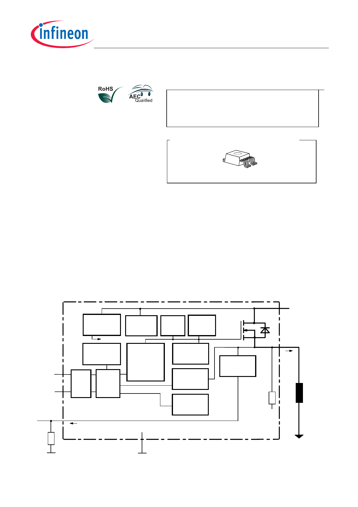
Smart Sense High-Side
Power Switch
Features
• Short circuit protection
• Current limitation
• Proportional load current sense
• CMOS compatible input
• Open drain diagnostic output
• Fast demagnetization of inductive loads
• Undervoltage and overvoltage shutdown with
auto-restart and hysteresis
• Overload protection
• Thermal shutdown
• Overvoltage protection including load dump (with
external GND-resistor)
• Reverse battery protection (with external GND-resistor)
• Loss of ground and loss of
V
bb
protection
• Electrostatic discharge (ESD) protection
Application
• µC compatible power switch with diagnostic feedback for 12 V and 24 V DC grounded loads
• All types of resistive, inductive and capacitve loads
• Replaces electromechanical relays, fuses and discrete circuits
General Description
N channel vertical power FET with charge pump, ground referenced CMOS compatible input and diagnostic
feedback, proportional sense of load current, monolithically integrated in Smart SIPMOS
technology.
Providing embedded protective functions.
Block Diagram
,1
67
(6'
/RJLF
9ROWDJH
VHQVRU
9ROWDJH
VRXUFH
&KDUJHSXPS
/HYHOVKLIWHU
7HPSHUDWXUH
VHQVRU
5HFWLILHU
/LPLWIRU
XQFODPSHG
LQGORDGV
*DWH
SURWHFWLRQ
&XUUHQW
OLPLW
6LJQDO*1'
*1'
9
/RJLF
2YHUYROWDJH
SURWHFWLRQ
9EE
352)(7
287
/RDG*1'
/RDG
*1'
52
&XUUHQW
6HQVH
2XWSXW
9ROWDJH
GHWHFWLRQ
5,6
,6
,
,6
,
/
Product Summary
Operating voltage
V
bb(on)
5.0 ... 34
V
On-state resistance
R
ON
30 m
Ω
Load current (ISO)
I
L(ISO)
12.6
A
Current limitation
I
L(SCr)
24
A
Package
TO220-7-11 TO263-7-2 TO220-7-12
1 1 1
Standard (staggered) SMD Straight
•
AEC qualified
•
Green product (RoHS compliant)
Data Sheet
1
V1.1, 2008-19-08
Smart High-Side Power Switch
BTS640S2G
Pin Symbol Function
1 ST
Diagnostic feedback: open drain, invers to input level
2 GND Logic
ground
3
IN
Input, activates the power switch in case of logical high signal
4 Vbb
Positive power supply voltage, the tab is shorted to this pin
5 IS
Sense current output, proportional to the load current, zero in
the case of current limitation of load current
6 & 7
OUT
(Load, L)
Output, protected high-side power output to the load.
Both output pins have to be connected in parallel for operation
according this spec (e.g. k
ILIS
).
Design the wiring for the max. short circuit current
Maximum Ratings at
T
j
= 25 °C unless otherwise specified
Parameter Symbol
Values
Unit
Supply voltage
(overvoltage protection see page 4)
V
bb
43
V
Supply voltage for full short circuit protection
T
j Start=-40 ...+150°C
V
bb
34
V
Load dump protection
1
) VLoadDump = VA + Vs, VA = 13.5V
R
I2)= 2 Ω,
R
L= 1 Ω,
t
d= 200 ms, IN= low or high
V
Load dump
3
)
60
V
Load current
(Short circuit current, see page 5)
I
L
self-limited
A
Operating temperature range
Storage temperature range
T
j
T
stg
-40 ...+150
-55 ...+150
°C
Power dissipation
(DC), TC ≤ 25 °C
P
tot
85
W
Inductive load switch-off energy dissipation, single pulse
Vbb = 12V,
T
j,start = 150°C,
T
C = 150°C const.
I
L
= 12.6 A, Z
L
= 4,2 mH, 0
Ω:
I
L
= 4 A, Z
L
= 330 mH, 0
Ω:
E
AS
E
AS
0,41
3,5
J
Electrostatic discharge capability (ESD)
IN:
(Human Body Model)
ST,
IS:
out to all other pins shorted:
acc. MIL-STD883D, method 3015.7 and ESD assn. std. S5.1-1993
R=1.5k
Ω; C=100pF
V
ESD
1.0
4.0
8.0
kV
Input voltage
(DC)
V
IN
-10 ... +16
V
Current through input pin
(DC)
Current through status pin
(DC)
Current through current sense pin
(DC)
see internal circuit diagrams page 8
I
IN
I
ST
I
IS
±2.0
±5.0
±14
mA
1
) Supply voltages higher than V
bb(AZ)
require an external current limit for the GND and status pins (a 150
Ω
resistor in the GND connection is recommended).
2)
R
I
= internal resistance of the load dump test pulse generator
3)
V
Load dump
is setup without the DUT connected to the generator according to ISO 7637-1 and DIN 40839
Data Sheet
2
V1.1, 2008-19-08
Smart High-Side Power Switch
BTS640S2G
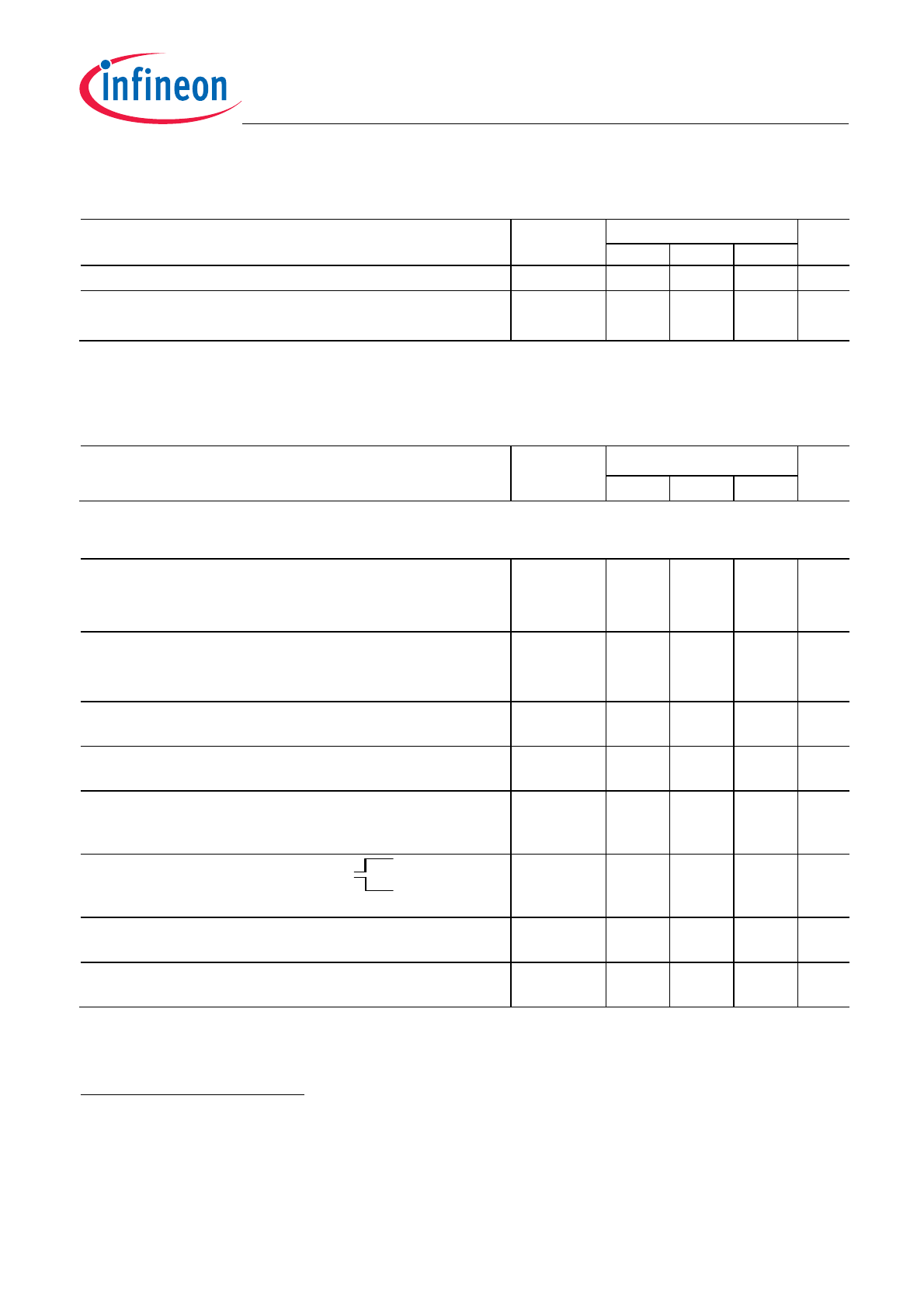
Thermal Characteristics
Parameter and Conditions
Symbol
Values
Unit
min typ
max
Thermal resistance
chip - case
:
R
thJC
-- --
1.47
K/W
junction - ambient (free air):
R
thJA
-- --
75
SMD version, device on PCB
4)
:
-- 33 --
4
) Device on 50mm*50mm*1.5mm epoxy PCB FR4 with 6cm
2
(one layer, 70
µm thick) copper area for Vbb
connection. PCB is vertical without blown air.
Electrical Characteristics
Parameter and Conditions
Symbol
Values
Unit
at
T
j
= 25 °C,
V
bb
= 12 V unless otherwise specified
min typ
max
Load Switching Capabilities and Characteristics
On-state resistance
(pin 4 to 6&7)
I
L = 5 A
T
j
=25 °C:
T
j
=150 °C:
R
ON
--
27
54
30
60
m
Ω
Output voltage drop limitation at small load
currents
(pin 4 to 6&7), see page 14
I
L = 0.5 A
T
j =-40...+150°C:
V
ON(NL)
--
50 --
mV
Nominal load current, ISO Norm
(pin 4 to 6&7)
V
ON = 0.5 V,
T
C = 85 °C
I
L(ISO)
11.4
12.6 --
A
Nominal load current, device on PCB
4)
T
A = 85 °C,
T
j ≤ 150 °C
V
ON ≤ 0.5 V,
I
L(NOM)
4.0
4.5 --
A
Output current (pin 6&7) while GND disconnected
or GND pulled up,
V
bb=30 V,
V
IN= 0, see diagram page
9; not subject to production test, specified by design
I
L(GNDhigh)
-- -- 8
mA
Turn-on time
IN
to 90%
V
OUT:
Turn-off time
IN
to 10%
V
OUT:
R
L = 12 Ω,
T
j =-40...+150°C
t
on
t
off
25
25
70
80
150
200
µs
Slew rate on
10 to 30%
V
OUT,
R
L = 12 Ω,
T
j =-40...+150°C
d
V /dt
on
0.1 -- 1
V/
µs
Slew rate off
70 to 40%
V
OUT,
R
L = 12 Ω,
T
j =-40...+150°C
-d
V/dt
off
0.1 -- 1
V/
µs
Data Sheet
3
V1.1, 2008-19-08
Smart High-Side Power Switch
BTS640S2G
Parameter and Conditions
Symbol
Values
Unit
at
T
j
= 25 °C,
V
bb
= 12 V unless otherwise specified
min typ
max
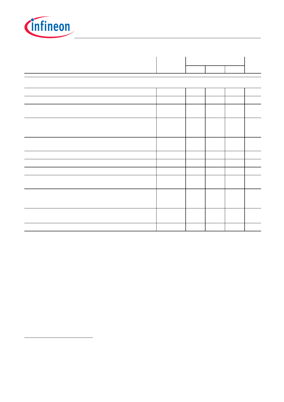
Operating Parameters
Operating voltage
5
)
T
j =-40...+150°C:
V
bb(on)
5.0
--
34
V
Undervoltage shutdown
T
j =-40...+150°C:
V
bb(under)
3.2 --
5.0
V
Undervoltage restart
Tj =-40...+25°C:
Tj =+150°C:
V
bb(u rst)
-- 4.5 5.5
6.0
V
Undervoltage restart of charge pump
see diagram page 13
Tj =-40...+25°C:
Tj =25...150°C:
V
bb(ucp)
--
--
4.7
--
6.5
7.0
V
Undervoltage hysteresis
∆
V
bb(under) =
V
bb(u rst) -
V
bb(under)
∆V
bb(under)
-- 0.5 --
V
Overvoltage shutdown
T
j =-40...+150°C:
V
bb(over)
34
--
43
V
Overvoltage restart
T
j =-40...+150°C:
V
bb(o rst)
33 -- --
V
Overvoltage hysteresis
T
j =-40...+150°C:
∆V
bb(over)
-- 1 --
V
Overvoltage protection
6
)
Tj =-40°C:
I
bb=40 mA
Tj =+25...+150°C
V
bb(AZ)
41
43
--
47
--
52
V
Standby current (pin 4)
V
IN=0
T
j
=-40...+25°C
:
T
j
= 150°C:
I
bb(off)
--
--
4
12
15
25
µA
Off state output current (included in
I
bb(off)
)
V
IN=0,
T
j =-40...+150°C:
I
L(off)
-- --
10
µA
Operating current
(Pin 2)7),
V
IN=5 V
I
GND
-- 1.2 3
mA
5
)
At supply voltage increase up to
V
bb
= 4.7 V typ without charge pump,
V
OUT
≈
V
bb
- 2 V
6)
Supply voltages higher than V
bb(AZ)
require an external current limit for the GND and status pins (a 150
Ω
resistor in the GND connection is recommended). See also
V
ON(CL)
in table of protection functions and
circuit diagram page 9.
7
)
Add
I
ST
, if
I
ST
> 0, add
I
IN
, if
V
IN
>5.5 V
Data Sheet
4
V1.1, 2008-19-08
Smart High-Side Power Switch
BTS640S2G

Parameter and Conditions
Symbol
Values
Unit
at
T
j
= 25 °C,
V
bb
= 12 V unless otherwise specified
min typ
max
Protection Functions
8)
Initial peak short circuit current limit
(pin 4 to 6&7)
I
L(SCp)
T
j
=-40°C:
T
j
=25°C:
T
j
=+150°C:
48
40
31
56
50
37
65
58
45
A
Repetitive short circuit shutdown current limit
I
L(SCr)
T
j =
T
jt (see timing diagrams, page 12)
--
24
--
A
Output clamp
(inductive load switch off)
at
V
OUT =
V
bb -
V
ON(CL);
I
L= 40 mA,
T
j
=-40°C:
T
j
=+25..+150°C:
V
ON(CL)
41
43
--
47
--
52
V
Thermal overload trip temperature
T
jt
150 -- --
°C
Thermal hysteresis
∆
T
jt
-- 10 --
K
Reverse battery
(pin 4 to 2)
9
)
-
V
bb
--
--
32
V
Reverse battery voltage drop
(Vout > Vbb)
I
L = -5 A
T
j=150 °C:
-V
ON(rev)
--
600 --
mV
Diagnostic Characteristics
Current sense ratio
10)
, static on-condition,
V
IS = 0...5 V,
V
bb(on) = 6.511)...27V,
k
ILIS =
I
L /
I
IS
T
j
= -40°C,
I
L
= 5 A:
k
ILIS
4550
5000
6000
T
j
= -40°C,
I
L
= 0.5 A:
3300 5000
8000
T
j
= 25...+150°C,
I
L
= 5 A:
,
T
j
= 25...+150°C,
I
L
= 0.5 A:
4550
4000
5000
5000
5550
6500
Current sense output voltage limitation
T
j = -40 ...+150°C
I
IS = 0,
I
L = 5 A:
V
IS(lim)
5.4
6.1
6.9
V
Current sense leakage/offset current
T
j = -40 ...+150°C
V
IN=0,
V
IS = 0,
I
L = 0:
I
IS(LL)
0
--
1
µA
V
IN=5 V,
V
IS = 0,
I
L = 0:
I
IS(LH)
0 --
15
V
IN=5 V,
V
IS = 0,
V
OUT = 0
(short circuit):
I
IS(SH)
12 )
0 --
10
8)
Integrated protection functions are designed to prevent IC destruction under fault conditions described in the
data sheet. Fault conditions are considered as "outside" normal operating range. Protection functions are not
designed for continuous repetitive operation.
9
) Requires
150
Ω resistor in GND connection. The reverse load current through the intrinsic drain-source
diode has to be limited by the connected load. Note that the power dissipation is higher compared to normal
operating conditions due to the voltage drop across the intrinsic drain-source diode. The temperature
protection is not active during reverse current operation! Input and Status currents have to be limited (see
max. ratings page 2 and circuit page 9).
10)
This range for the current sense ratio refers to all devices. The accuracy of the
k
ILIS
can be raised at least by
a factor of two by matching the value of
k
ILIS
for every single device.
In the case of current limitation the sense current
I
IS
is zero and the diagnostic feedback potential
V
ST
is
High. See figure 2b, page 11.
11)
Valid if
V
bb(u rst)
was exceeded before.
12)
not subject to production test, specified by design
Data Sheet
5
V1.1, 2008-19-08
Smart High-Side Power Switch
BTS640S2G
BTS 640 S2
Parameter and Conditions
Symbol
Values
Unit
at
T
j
= 25 °C,
V
bb
= 12 V unless otherwise specified
min typ
max
Current sense settling time to
I
IS static
±10% after
positive input slope
13
)
,
I
L = 0
5 A,
T
j= -40...+150°C
t
son(IS)
--
--
300
µs
Current sense settling time to 10% of
I
IS
static after
negative input slope
13
) ,
I
L = 5
0 A ,
T
j= -40...+150°C
t
soff(IS)
--
30
100
µs
Current sense rise time (60% to 90%) after change
of load current
13
)
,
I
L = 2.5
5 A
t
slc(IS)
--
10
--
µs
Open load detection voltage
14
)
(off-condition)
T
j=-40..150°C:
V
OUT(OL)
2 3
4
V
Internal output pull down
(pin 6 to 2),
V
OUT=5 V,
T
j=-40..150°C
R
O
5
15 40
k
Ω
Input and Status Feedback
15
)
Input resistance
see circuit page 8
R
I
3,0
4,5 7,0
k
Ω
Input turn-on threshold voltage
T
j =-40..+150
°
C
:
V
IN(T+)
-- --
3.5
V
Input turn-off threshold voltage
T
j =-40..+150
°
C
:
V
IN(T-)
1.5 -- --
V
Input threshold hysteresis
∆ V
IN(T)
-- 0.5 --
V
Off state input current
(pin 3),
V
IN = 0.4 V
T
j =-40..+150°C
I
IN(off)
1
-- 50
µA
On state input current
(pin 3),
V
IN = 5 V
T
j =-40..+150°C
I
IN(on)
20
50 90
µA
Delay time for status with open load
after Input neg. slope (see diagram page 13)
t
d(ST OL3)
--
400
--
µs
Status delay after positive input slope
13
)
Tj=-40 ... +150°C:
t
don(ST)
--
13
--
µs
Status delay after negative input
slope
13
)
Tj=-40 ... +150°C:
t
doff(ST)
--
1
--
µs
Status output (open drain)
Zener limit voltage
T
j
=-40...+150°C,
I
ST
= +1.6 mA:
ST low voltage
T
j
=-40...+25°C,
I
ST
= +1.6 mA:
T
j
= +150°C,
I
ST
= +1.6 mA:
V
ST(high)
V
ST(low)
5.4
--
--
6.1
--
--
6.9
0.4
0.7
V
Status leakage current,
V
ST = 5 V,
T
j=25 ... +150°C:
I
ST(high)
--
--
2
µA
13)
not subject to production test, specified by design
14)
External pull up resistor required for open load detection in off state.
15)
If a ground resistor R
GND
is used, add the voltage drop across this resistor.
Data Sheet
6
V1.1, 2008-19-08
Smart High-Side Power Switch
BTS640S2G

Truth Table
Input Output Status
Current
Sense
level
level level
IIS
Normal
operation
L
H
L
H
H
L
0
nominal
Current-
limitation
L
H
L
H
H
H
0
0
Short circuit to
GND
L
H
L
L
16)
H
H
0
0
Over-
temperature
L
H
L
L
H
H
0
0
Short circuit to
V
bb
L
H
H
H
L
17)
L
0
<nominal
18)
Open load
L
H
L
19)
H
H (L
20)
)
L
0
0
Undervoltage L
H
L
L
H
L
0
0
Overvoltage L
H
L
L
H
L
0
0
Negative output
voltage clamp
L L H
0
L = "Low" Level
X = don't care
Z = high impedance, potential depends on external circuit
H = "High" Level
Status signal after the time delay shown in the diagrams (see fig 5. page 12...13)
16
) The voltage drop over the power transistor is
V
bb
-
V
OUT
>typ.3V. Under this condition the sense current
I
IS
is
zero
17)
An external short of output to V
bb
, in the off state, causes an internal current from output to ground. If R
GND
is used, an offset voltage at the GND and ST pins will occur and the V
ST low
signal may be errorious.
18
) Low ohmic short to
V
bb
may reduce the output current
I
L
and therefore also the sense current
I
IS
.
19
) Power Transistor off, high impedance
20
) with external resistor between pin 4 and pin 6&7
Data Sheet
7
V1.1, 2008-19-08
Smart High-Side Power Switch
BTS640S2G
Terms
352)(7
9
,6
67
287
*1'
EE
967
9,1
,67
, ,1
9EE
,EE
,*1'
,1
9,6
, ,6
9287
921
,/
287
5 *1'
Input circuit (ESD protection)
,1
*1'
,
5
(6'='
,,
,
The use of ESD zener diodes as voltage clamp at DC
conditions is not recommended.
Status output
67
*1'
(6'
='
9
5
6721
ESD-Zener diode: 6.1 V typ., max 5 mA;
R
ST(ON)
< 440
Ω at 1.6 mA,
The use of ESD zener
diodes as voltage clamp at DC conditions is not
recommended.
Current sense output
,6
*1'
,6
5
,6
,
(6'='
,6
9
ESD-Zener diode: 6.1 V typ., max 14 mA;
R
IS
= 1 k
Ω nominal
Inductive and overvoltage output clamp
9EE
287
*1'
352)(7
9=
9
21
V
ON
clamped to 47 V typ.
Data Sheet
8
V1.1, 2008-19-08
Smart High-Side Power Switch
BTS640S2G
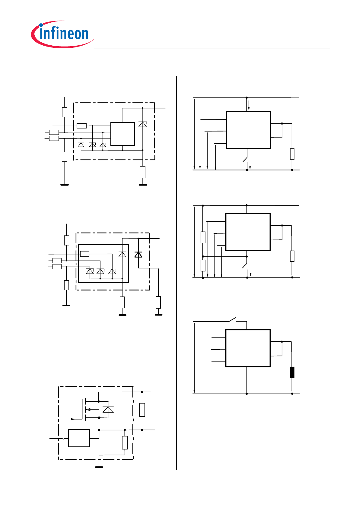
Overvoltage protection of logic part
9EE
,6
67
5
*1'
*1'
5
6LJQDO*1'
/RJLF
9=
,1
5,
9=
67
,6
5
9
9
5
V
Z1
= 6.1 V typ.,
V
Z2
= 47 V typ.,
R
I
= 4 k
Ω typ,
R
GND
= 150
Ω, R
ST
= 15 k
Ω, R
IS
= 1 k
Ω, R
V
= 15 k
Ω,
Reverse battery protection
*1'
/RJLF
,6
67
5
,1
67
,6
5
9
9
5
287
/
5
3RZHU*1'
*1'
5
6LJQDO*1'
3RZHU
,QYHUVH
,
5
9EE
'LRGH
=
9
The load
R
L
is inverse on, temperature protection is
not active
R
GND
= 150
Ω, R
I
= 4 k
Ω typ, R
ST
≥ 500 Ω, R
IS
≥ 200 Ω,
R
V
≥ 500 Ω,
Open-load detection
OFF-state diagnostic condition:
V
OUT
> 3 V typ.; IN low
/RJLF
67
2XW
9287
6LJQDO*1'
5(;7
52
2))
9EE
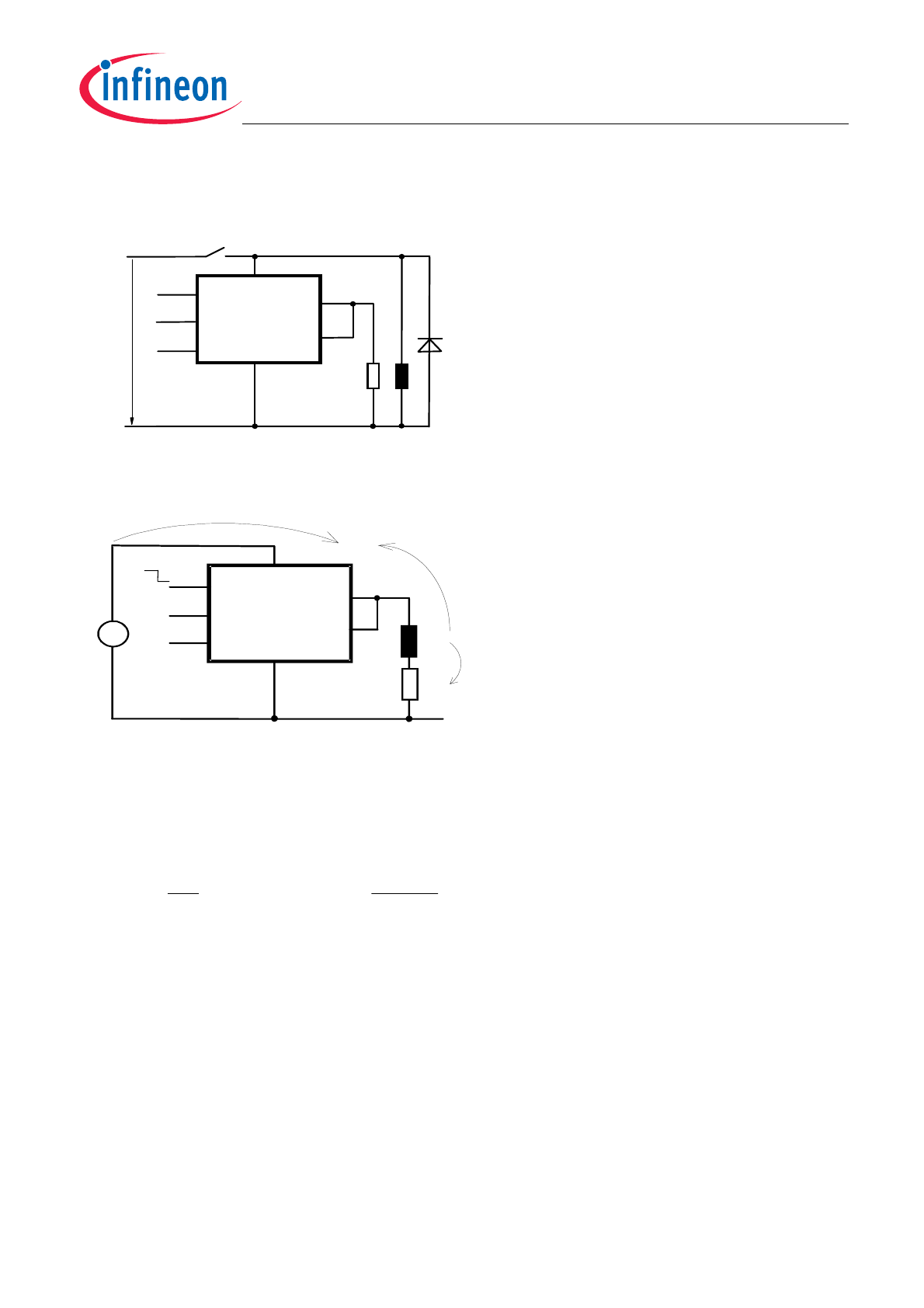
GND disconnect
352)(7
9
67
,6
287
*1'
EE
9EE
,EE
,1
287
9,1 967 9,6
9
*1'
Any kind of load. In case of Input=high is
V
OUT
≈
V
IN
-
V
IN(T+)
.
Due to V
GND
>0, no V
ST
= low signal available.
GND disconnect with GND pull up
352)(7
9
67
,6
287
*1'
EE
9EE
,1
287
9,19679,6
9*1'
Any kind of load. If V
GND >
V
IN
-
V
IN(T+)
device stays off
Due to V
GND
>0, no V
ST
= low signal available.
V
bb
disconnect with energized inductive
load
352)(7
9
67
,6
287
*1'
EE
9EE
,1
287
KLJK
Normal load current can be handled by the PROFET
itself.
Data Sheet
9
V1.1, 2008-19-08
Smart High-Side Power Switch
BTS640S2G
V
bb
disconnect with charged external
inductive load
352)(7
9
67
,6
287
*1'
EE
,1
287
9EE
KLJK
'
5
/
/
If other external inductive loads L are connected to the PROFET,
additional elements like D are necessary.
Inductive Load switch-off energy
dissipation
352)(7
,1
67
287
*1'
9EE
(
(
(
($6
EE
/
5
(/RDG
,6
287
9EE
Energy stored in load inductance:
E
L
=
1/2
·
L
·
I
2
L
While demagnetizing load inductance, the energy
dissipated in PROFET is
E
AS
= E
bb
+ E
L
- E
R
=
V
ON(CL)
·
i
L
(t) dt,
with an approximate solution for R
L
> 0 Ω:
E
AS
=
I
L
·
L
2
·
R
L
·
(
V
bb
+ |V
OUT(CL)
|)
·
OQ
(1+
I
L
·
R
L
|V
OUT(CL)
|
)
Data Sheet
10
V1.1, 2008-19-08
Smart High-Side Power Switch
BTS640S2G