

HITFET - BTS3205N
Smart Low-Side Power Switch
Data Sheet, Rev. 1.1, September 2011
Automotive Power

Smart Low-Side Power Switch
BTS3205N
Data Sheet
2
Rev. 1.1, 2011-09-01
1
Overview . . . . . . . . . . . . . . . . . . . . . . . . . . . . . . . . . . . . . . . . . . . . . . . . . . . . . . . . . . . . . . . . . . . . . . . 3
2
Block Diagram . . . . . . . . . . . . . . . . . . . . . . . . . . . . . . . . . . . . . . . . . . . . . . . . . . . . . . . . . . . . . . . . . . . 5
2.1
Terms . . . . . . . . . . . . . . . . . . . . . . . . . . . . . . . . . . . . . . . . . . . . . . . . . . . . . . . . . . . . . . . . . . . . . . . . . . 5
3
Pin Configuration . . . . . . . . . . . . . . . . . . . . . . . . . . . . . . . . . . . . . . . . . . . . . . . . . . . . . . . . . . . . . . . . 6
3.1
Pin Assignment BTS3205N . . . . . . . . . . . . . . . . . . . . . . . . . . . . . . . . . . . . . . . . . . . . . . . . . . . . . . . . . 6
3.2
Pin Definitions and Functions . . . . . . . . . . . . . . . . . . . . . . . . . . . . . . . . . . . . . . . . . . . . . . . . . . . . . . . . 6
4
General Product Characteristics . . . . . . . . . . . . . . . . . . . . . . . . . . . . . . . . . . . . . . . . . . . . . . . . . . . . 7
4.1
Absolute Maximum Ratings . . . . . . . . . . . . . . . . . . . . . . . . . . . . . . . . . . . . . . . . . . . . . . . . . . . . . . . . . 7
4.2
Thermal Resistance . . . . . . . . . . . . . . . . . . . . . . . . . . . . . . . . . . . . . . . . . . . . . . . . . . . . . . . . . . . . . . . 8
4.2.1
Transient Thermal Impedance . . . . . . . . . . . . . . . . . . . . . . . . . . . . . . . . . . . . . . . . . . . . . . . . . . . . . . 8
5
Block Description and Characteristics . . . . . . . . . . . . . . . . . . . . . . . . . . . . . . . . . . . . . . . . . . . . . . 10
5.1
Input and Power Stage . . . . . . . . . . . . . . . . . . . . . . . . . . . . . . . . . . . . . . . . . . . . . . . . . . . . . . . . . . . . 10
5.1.1
Input Circuit . . . . . . . . . . . . . . . . . . . . . . . . . . . . . . . . . . . . . . . . . . . . . . . . . . . . . . . . . . . . . . . . . . . 10
5.1.2
Failure Feedback . . . . . . . . . . . . . . . . . . . . . . . . . . . . . . . . . . . . . . . . . . . . . . . . . . . . . . . . . . . . . . . 11
5.1.3
Output On-State Resistance . . . . . . . . . . . . . . . . . . . . . . . . . . . . . . . . . . . . . . . . . . . . . . . . . . . . . . 11
5.1.4
Power Dissipation . . . . . . . . . . . . . . . . . . . . . . . . . . . . . . . . . . . . . . . . . . . . . . . . . . . . . . . . . . . . . . 12
5.1.5
Output Timing . . . . . . . . . . . . . . . . . . . . . . . . . . . . . . . . . . . . . . . . . . . . . . . . . . . . . . . . . . . . . . . . . 12
5.1.6
Characteristics . . . . . . . . . . . . . . . . . . . . . . . . . . . . . . . . . . . . . . . . . . . . . . . . . . . . . . . . . . . . . . . . . 13
6
Protection Functions . . . . . . . . . . . . . . . . . . . . . . . . . . . . . . . . . . . . . . . . . . . . . . . . . . . . . . . . . . . . 15
6.1
Thermal Protection . . . . . . . . . . . . . . . . . . . . . . . . . . . . . . . . . . . . . . . . . . . . . . . . . . . . . . . . . . . . . . . 15
6.2
Overvoltage Protection . . . . . . . . . . . . . . . . . . . . . . . . . . . . . . . . . . . . . . . . . . . . . . . . . . . . . . . . . . . . 15
6.3
Short Circuit Protection . . . . . . . . . . . . . . . . . . . . . . . . . . . . . . . . . . . . . . . . . . . . . . . . . . . . . . . . . . . . 17
6.4
Characteristics . . . . . . . . . . . . . . . . . . . . . . . . . . . . . . . . . . . . . . . . . . . . . . . . . . . . . . . . . . . . . . . . . . 18
7
Package Outlines BTS3205N . . . . . . . . . . . . . . . . . . . . . . . . . . . . . . . . . . . . . . . . . . . . . . . . . . . . . . 19
8
Revision History . . . . . . . . . . . . . . . . . . . . . . . . . . . . . . . . . . . . . . . . . . . . . . . . . . . . . . . . . . . . . . . . 20
PG-SOT-223-4
Type
Package
Marking
BTS3205N
PG-SOT-223-4
3205N
Data Sheet
3
Rev. 1.1, 2011-09-01
Smart Low-Side Power Switch
HITFET
BTS3205N
1
Overview
Features
•
Logic Level input
•
Short circuit and Overload protection
•
Current limitation
•
Input protection (ESD)
•
Thermal protection with auto restart
•
Compatible to standard Power MOSFET
•
Analog driving possible
•
Green Product (RoHS compliant)
•
AEC Qualified
Description
The BTS3205N is a one channel low-side power switch in PG-SOT-223-4 package providing embedded protective
functions. The device is monolithic integrated and consist of an N-channel power MOSFET transistor and
additional protection circuitry.
Table 1
Product Summary
Drain Voltage
V
D
42 V
1)
1) Active clamped
Input Voltage
V
IN(max)
10 V
Typical On-State Resistance at
T
j
= 25
°C and Vin = 10V
R
DS(ON,amb typ)
0.7
Ω
Maximum On-State Resistance at
T
j
= 150
°C and Vin = 10V
R
DS(ON,hot max)
1.9
Ω
Nominal Load Current
I
Dnom(min)
350 mA
Drain Current
I
D
600 mA
2)
2) Internally limited
Single Clamping Energy
E
AS
65 mJ

Smart Low-Side Power Switch
BTS3205N
Overview
Data Sheet
4
Rev. 1.1, 2011-09-01
Protective Functions
•
Electrostatic discharge protection (ESD)
•
Active clamp over voltage protection
•
Thermal shutdown with auto restart
•
Short circuit protection
Fault Information
•
Thermal shutdown
•
Short to Battery and overload
Applications
•
Designed for driving Relays in Automotive Applications
•
All types of resistive, inductive and capacitive loads
•
Suitable for loads with peak currents
•
Replaces discrete circuits
Detailed Description
The device is able to switch all kind of resistive, inductive and capacitive loads, limited by
E
AS
and maximum
current capabilities.
The BTS3205N offers ESD protection of the IN Pin in relation to the Source Pin.
The overtemperature protection prevents the device from overheating due to overload and/or bad cooling
conditions. The temperature information is given by a temperature sensor in the power MOSFET. During thermal
shutdown the device tries to sink an increased input current to feedback the fault condition.
The BTS3205N has a thermal-auto-restart function, the device will turn on again after the measured temperature
has dropped down for the thermal hysteresis.
The over voltage protection is active during load-dump or inductive turn off conditions. The power MOSFET is
limiting the Drain - Source voltage to the defined clamping voltage. This function is available regardless of the input
pin state.
Data Sheet
5
Rev. 1.1, 2011-09-01
Smart Low-Side Power Switch
BTS3205N
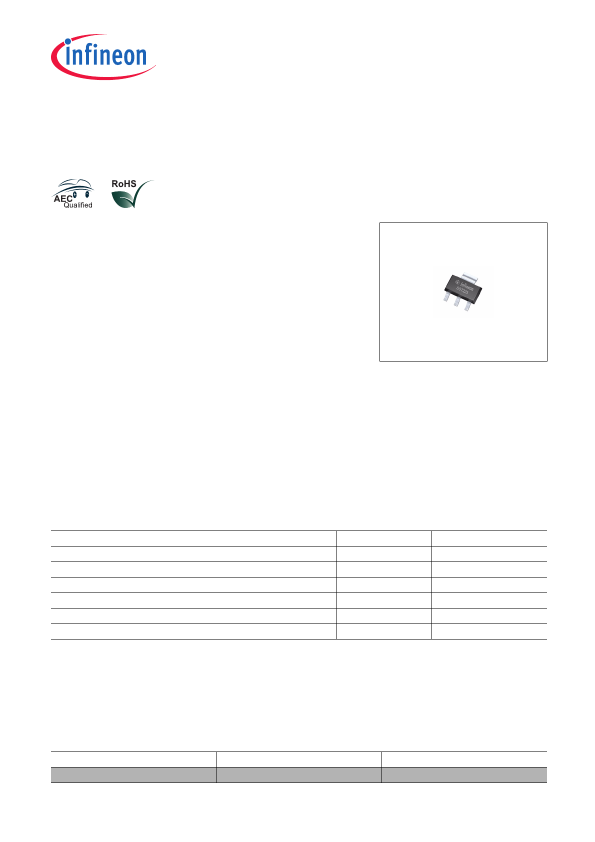
Block DiagramTerms
2
Block Diagram
Figure 1
Block Diagram
2.1
Terms
Figure 2
shows all external terms used in this data sheet.
Figure 2
Terms
Drain
Source
Over-
voltage
Protection
IN
Gate
Driving
Unit
ESD
Protection
BlockDiagram _3205N.emf
Over-
temperature
Protection
Overload
detection and
Current limiter
Terms.emf
V
IN
V
D
Source
I
S
Drain
V
bb
R
L
IN
I
D
I
IN
V
bb
GND
R
in
BTS3205N

Smart Low-Side Power Switch
BTS3205N
Pin ConfigurationPin Assignment BTS3205N
Data Sheet
6
Rev. 1.1, 2011-09-01
3
Pin Configuration
3.1
Pin Assignment BTS3205N
Figure 3
Pin Configuration PG-SOT-223-4
3.2
Pin Definitions and Functions
Pin
Symbol
Function
1
IN
Input / fault feedback
2, 4
Drain
Load connection
3
Source
Ground connection
1
IN
2
DRAIN
3
SOURCE
DRAIN (TAB)
4
Pin_SOT 223.emf

Data Sheet
7
Rev. 1.1, 2011-09-01
Smart Low-Side Power Switch
BTS3205N
General Product CharacteristicsAbsolute Maximum Ratings
4
General Product Characteristics
4.1
Absolute Maximum Ratings
Absolute Maximum Ratings
1)
T
j
= -40
⋅C to +150 ⋅C; all voltages with respect to ground, positive current flowing into pin
(unless otherwise specified)
1) Not subject to production test, specified by design.
Pos.
Parameter
Symbol Limit Values Unit
Test Conditions
Min.
Max.
Voltages
4.1.1
Drain voltage
V
D
–
42
V
2)
V
IN
= 0 V,
I
D
= 10 mA
2) Active clamped.
4.1.2
Input Voltage
V
IN
-0.2
10
V
–
4.1.3
Input Current
I
IN
self limited
mA
-0.2 V <
V
IN
< 10 V
4.1.4
-2
2
mA
V
IN
< -0.2 V
or
V
IN
> 10 V
4.1.5
Drain Current
I
D
–
600
mA
3)
T
j
= 25
°C
3) Internally limited.
Energies
4.1.6
Unclamped single pulse inductive energy
single pulse
E
AS
0
65
mJ
I
D
= 350 mA;
V
bb
= 28 V;
T
J(start)
= 85
°C
4.1.7
Unclamped single pulse inductive energy
single pulse
–
30
mJ
I
D
= 250 mA;
V
bb
= 28 V;
T
J(start)
= 150
°C
4.1.8
Unclamped repetitive pulse inductive
energy 1
×10
4
cycles
E
AR
0
18
mJ
I
D
= 200 mA;
V
bb
= 13.5 V;
T
J(start)
= 105
°C
4.1.9
Unclamped repetitive pulse inductive
energy 1
×10
6
cycles
–
13
mJ
I
D
= 170 mA;
V
bb
= 13.5 V;
T
J(start)
= 105
°C
4.1.10
Total Power Dissipation
P
tot
–
0.78
W
4)
T
a
= 85
°C
4) Device mounted on PCB according EIA/JEDEC standard JESD51-7 (4-layer FR4, 76.2 mm
× 114.3 mm with buried
planes). PCB is mounted vertical without blown air.
Temperatures
4.1.11
Operating temperature
T
J
-40
+150
°C
–
4.1.12
Storage temperature
T
stg
-55
+150
°C
–
ESD Susceptibility
4.1.13
Electrostatic discharge voltage
5)
5) ESD susceptibility HBM according to EIA/JESD 22-A 114B, section 4.
V
ESD
-2
2
kV
IN Pin
R
= 1.5 k
;
C
= 100 pF;
T
J
= 25
°C

Smart Low-Side Power Switch
BTS3205N
General Product CharacteristicsThermal Resistance
Data Sheet
8
Rev. 1.1, 2011-09-01
4.2
Thermal Resistance
Note: Stresses above the ones listed here may cause permanent damage to the device. Exposure to absolute
maximum rating conditions for extended periods may affect device reliability.
Note: Integrated protection functions are designed to prevent IC destruction under fault conditions described in the
data sheet. Fault conditions are considered as “outside” normal operating range. Protection functions are
not designed for continuous repetitive operation.
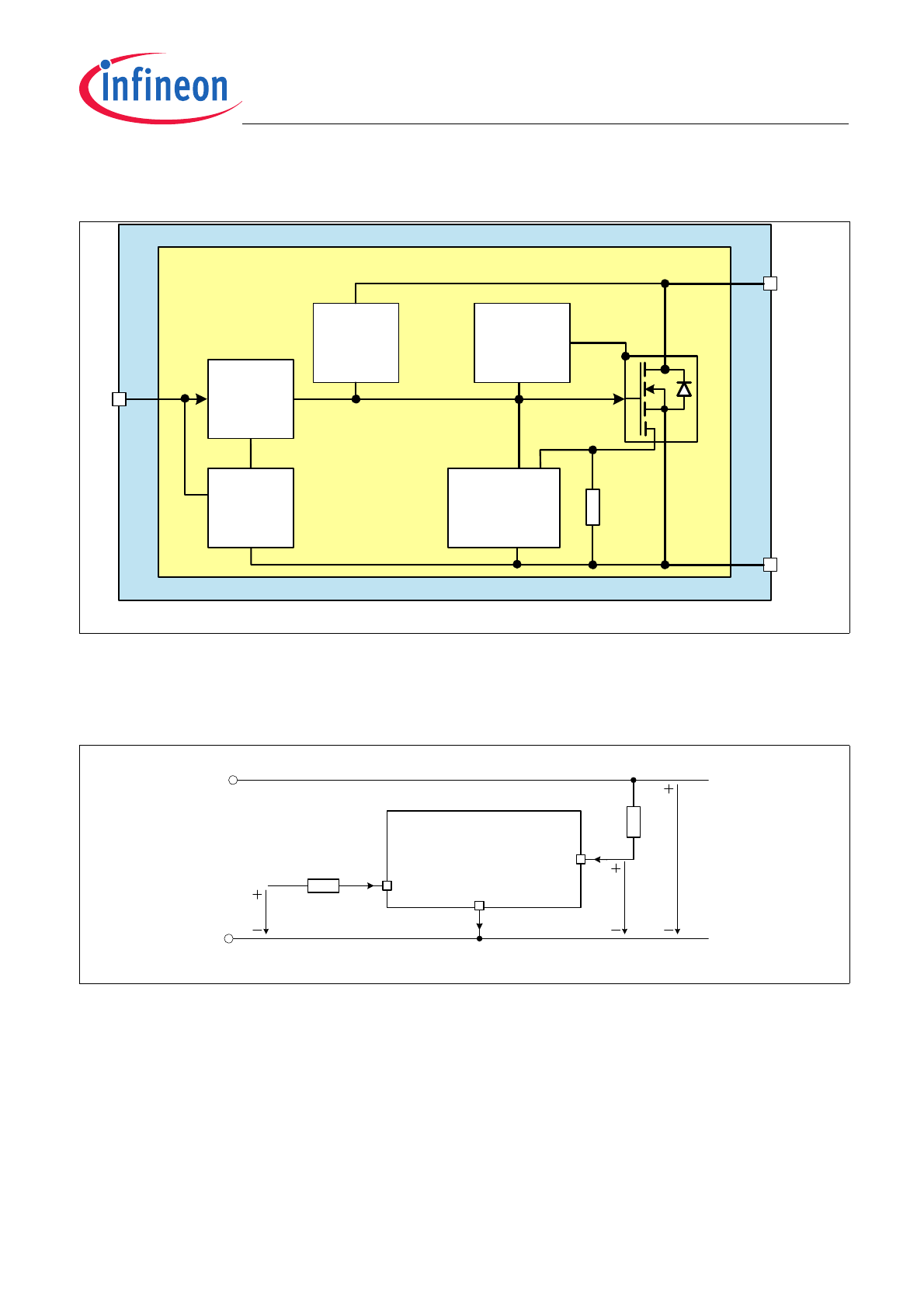
4.2.1
Transient Thermal Impedance
Figure 4
Typical Transient Thermal Impedance single pulse,
Z
thJA
and
Z
thJC
Pos.
Parameter
Symbol
Limit Values
Unit
Conditions
Min.
Typ.
Max.
4.2.1
Junction to Soldering Point
R
thJC
–
–
42
K/W
1)
2)
1) Not subject to production test, specified by design.
2) Device mounted on PCB according EIA/JEDEC standard JESD51-7 (4-layer FR4, 76.2 mm
× 114.3 mm with buried
planes). PCB is mounted vertical without blown air with 0.78W power dissipation generated on the DMOS.
4.2.2
Junction to Ambient
R
thJA
–
63
–
K/W
1)
2)
Zth_3205 N.emf
10
1
1
10
-1
10
-2
10
2
10
3
10
-3
10
-4
10
-5
15
0
30
45
60
75
90
Zt
h
[
K
/
W
]
t
p
[ s ]
Z
thJC
Z
thJA
Data Sheet
9
Rev. 1.1, 2011-09-01
Smart Low-Side Power Switch
BTS3205N
General Product CharacteristicsThermal Resistance
Figure 5
Typical Transient Thermal Impedance
Z
thJA
with different Duty cycles
Z
thJA
= f(t
p
) , D = tp/T, T
a
= 25 °C
Device mounted on PCB according EIA/JEDEC standard JESD51-7 (4-layer FR4, 76.2 mm
× 114.3 mm with
buried planes). PCB is mounted vertical without blown air with 0.78W power dissipation generated for single
pulse on the DMOS
Z
th
J
A
[K
/W
]
10
-3
10
-2
10
-1
10
-1
10
-6
10
-5
10
-4
t
p
[s]
10
2
1
10
1
10
3
10
2
10
1
1
D = 0.5
D = 0.2
D = 0.1
D = 0.05
D = 0.02
D = 0.01
Single pulse
pulse_BTS3205 N.emf
Smart Low-Side Power Switch
BTS3205N
Block Description and CharacteristicsInput and Power Stage
Data Sheet
10
Rev. 1.1, 2011-09-01
5
Block Description and Characteristics
5.1
Input and Power Stage
5.1.1
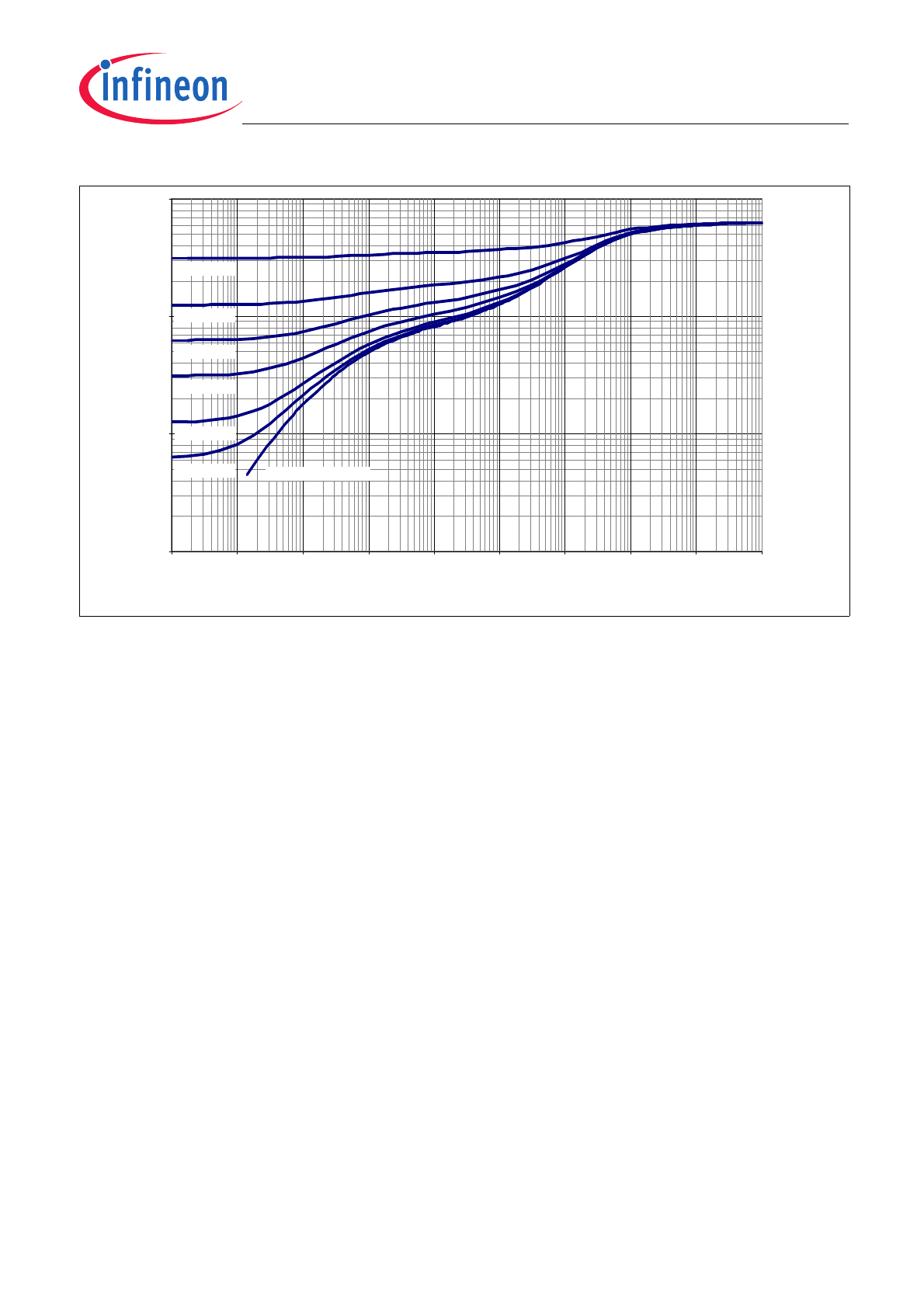
Input Circuit
Figure 6
shows the input circuit of the BTS3205N. The zener Diode protects the input circuit against ESD pulses.
The internal circuitry is supplied by the input PIN. During normal operation the Input is connected to the Gate of
the power MOSFET. During fault condition the device tries to sink the current
I
INlim
in order to give the fault
information back to the driving circuit.
Figure 6
Input Circuit
Figure 7
Typical Input Threshold Voltage
V
inth
= f(
T
J
);
I
D
= 50
μA,
V
D
=
V
IN
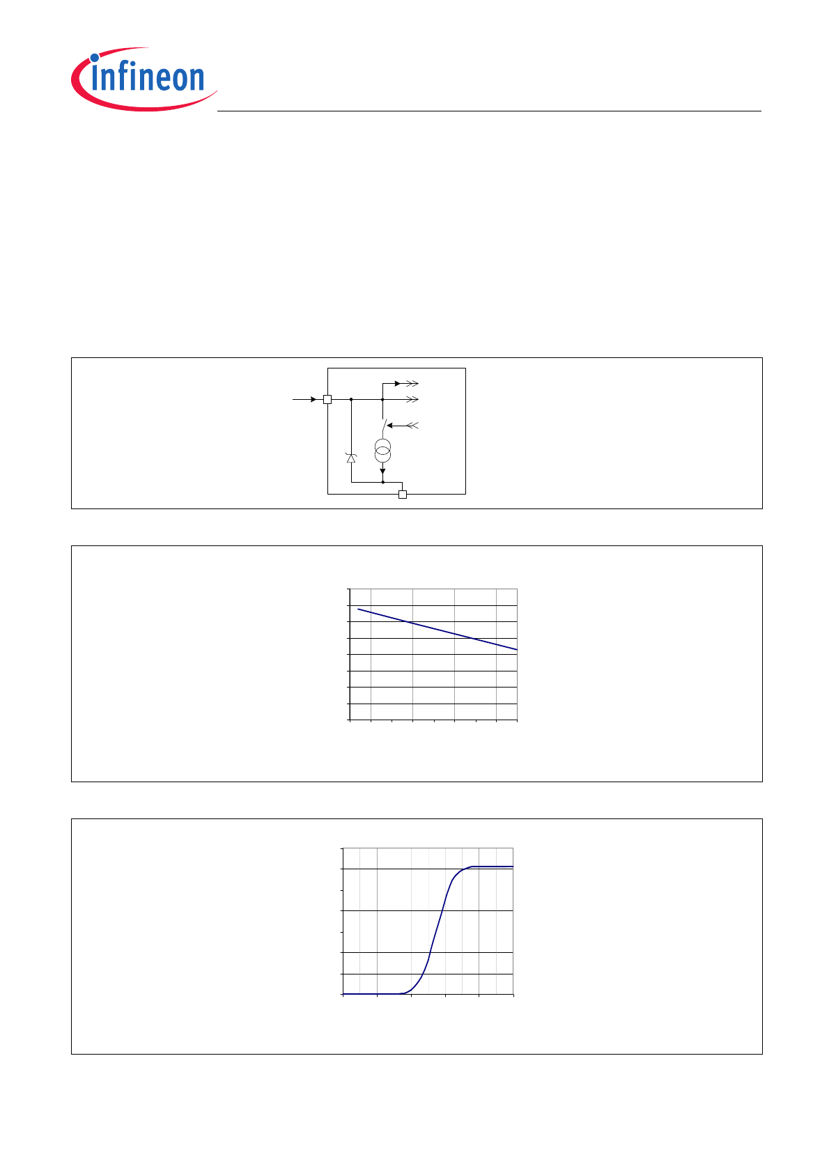
Figure 8
Typical Transfer Characteristic
I
D
= f(
V
IN
);
V
D
= 12 V,
T
Jstart
= 25 °C
Input.emf
Source
Z
D
IN
I
IN
Gate
Fault
condition
I
INlim
I
INnom
Logic
0,00
0,25
0,50
0,75
1,00
1,25
1,50
1,75
2,00
-50
-25
0
25
50
75
100 125 150
V
IN
(t
h)
[
V
]
T [°C]
Vinth.emf
0
0,1
0,2
0,3
0,4
0,5
0,6
0,7
0
1
2
3
4
5
I
D
[ A
]
V
IN
[ V ]
Transferchar.emf