

Automotive Power
Datasheet
Rev. 1.0, 2015-02-11
BTS3018TC
18 mOhm single channel smart low side power switch for 12V & 24V Application
HITFET
Smart Low Side Power Switch

Datasheet
2
Rev. 1.0, 2015-02-11
HITFET - BTS3018TC
Smart low side power switch
1
Overview . . . . . . . . . . . . . . . . . . . . . . . . . . . . . . . . . . . . . . . . . . . . . . . . . . . . . . . . . . . . . . . . . . . . . . . 3
2
Block Diagram . . . . . . . . . . . . . . . . . . . . . . . . . . . . . . . . . . . . . . . . . . . . . . . . . . . . . . . . . . . . . . . . . . . 5
2.1
Terms . . . . . . . . . . . . . . . . . . . . . . . . . . . . . . . . . . . . . . . . . . . . . . . . . . . . . . . . . . . . . . . . . . . . . . . . . . 5
3
Pin Configuration . . . . . . . . . . . . . . . . . . . . . . . . . . . . . . . . . . . . . . . . . . . . . . . . . . . . . . . . . . . . . . . . 6
3.1
Pin Assignment BTS3018TC . . . . . . . . . . . . . . . . . . . . . . . . . . . . . . . . . . . . . . . . . . . . . . . . . . . . . . . . 6
3.2
Pin Definitions and Functions . . . . . . . . . . . . . . . . . . . . . . . . . . . . . . . . . . . . . . . . . . . . . . . . . . . . . . . . 6
4
General Product Characteristics . . . . . . . . . . . . . . . . . . . . . . . . . . . . . . . . . . . . . . . . . . . . . . . . . . . . 7
4.1
Absolute Maximum Ratings . . . . . . . . . . . . . . . . . . . . . . . . . . . . . . . . . . . . . . . . . . . . . . . . . . . . . . . . . 7
4.2
Functional Range -- some values are links to other values in document . . . . . . . . . . . . . . . . . . . . . . . 8
4.3
Thermal Resistance . . . . . . . . . . . . . . . . . . . . . . . . . . . . . . . . . . . . . . . . . . . . . . . . . . . . . . . . . . . . . . . 8
4.3.1
Transient Thermal Impedance (Zth) . . . . . . . . . . . . . . . . . . . . . . . . . . . . . . . . . . . . . . . . . . . . . . . . . 9
4.4
Package. . . . . . . . . . . . . . . . . . . . . . . . . . . . . . . . . . . . . . . . . . . . . . . . . . . . . . . . . . . . . . . . . . . . . . . . . 9
5
Input and Power Stage . . . . . . . . . . . . . . . . . . . . . . . . . . . . . . . . . . . . . . . . . . . . . . . . . . . . . . . . . . . 10
5.1
Input Circuit . . . . . . . . . . . . . . . . . . . . . . . . . . . . . . . . . . . . . . . . . . . . . . . . . . . . . . . . . . . . . . . . . . . . . 10
5.1.1
Failure Feedback . . . . . . . . . . . . . . . . . . . . . . . . . . . . . . . . . . . . . . . . . . . . . . . . . . . . . . . . . . . . . . . 11
5.2
Power stage . . . . . . . . . . . . . . . . . . . . . . . . . . . . . . . . . . . . . . . . . . . . . . . . . . . . . . . . . . . . . . . . . . . . 11
5.2.1
Output On-state Resistance . . . . . . . . . . . . . . . . . . . . . . . . . . . . . . . . . . . . . . . . . . . . . . . . . . . . . . 11
5.2.2
Output Timing . . . . . . . . . . . . . . . . . . . . . . . . . . . . . . . . . . . . . . . . . . . . . . . . . . . . . . . . . . . . . . . . . 13
5.3
Characteristics . . . . . . . . . . . . . . . . . . . . . . . . . . . . . . . . . . . . . . . . . . . . . . . . . . . . . . . . . . . . . . . . . . 14
6
Protection Functions . . . . . . . . . . . . . . . . . . . . . . . . . . . . . . . . . . . . . . . . . . . . . . . . . . . . . . . . . . . . 17
6.1
Thermal Protection . . . . . . . . . . . . . . . . . . . . . . . . . . . . . . . . . . . . . . . . . . . . . . . . . . . . . . . . . . . . . . . 17
6.2
Overvoltage Protection . . . . . . . . . . . . . . . . . . . . . . . . . . . . . . . . . . . . . . . . . . . . . . . . . . . . . . . . . . . . 19
6.3
Short Circuit Protection . . . . . . . . . . . . . . . . . . . . . . . . . . . . . . . . . . . . . . . . . . . . . . . . . . . . . . . . . . . . 20
6.4
Characteristics . . . . . . . . . . . . . . . . . . . . . . . . . . . . . . . . . . . . . . . . . . . . . . . . . . . . . . . . . . . . . . . . . . 21
7
Package Outlines BTS3018TC . . . . . . . . . . . . . . . . . . . . . . . . . . . . . . . . . . . . . . . . . . . . . . . . . . . . . 22
8
Revision History . . . . . . . . . . . . . . . . . . . . . . . . . . . . . . . . . . . . . . . . . . . . . . . . . . . . . . . . . . . . . . . . 23
PG-TO263-3-2
Type
Package
Marking
BTS3018TC
PG-TO263-3-2
3018TC
Datasheet
3
Rev. 1.0, 2015-02-11
HITFET - BTS3018TC
Smart low side power switch
BTS3018TC
1
Overview
Features
•
Short circuit and over load protection
•
Thermal shutdown with latchbehavior
•
ESD protection
•
Over voltage protection
•
Logic level input suitable for 5V and 3.3V
•
Analog driving possible
•
12V and 24V usability
•
Green Product (RoHS compliant)
•
AEC Qualified
Description
The BTS3018TC is a single channel low-side MOSFET power switch in PG-TO263-3-2 (D²PAK) package
providing embedded protective functions.
The device is monolithically integrated with a N channel vertical power FET and embedded protection functions.
The BTS3018TC is automotive qualified and can be used in 12V and 24V automotive and industrial applications.
Protective Functions
•
Electrostatic discharge protection (ESD)
•
Active clamp over voltage protection
•
Thermal shutdown with latching behavior
•
Over load and Short circuit protection
•
Current limitation
Table 1
Product Summary
Output voltage
1)
1) Active clamped
V
OUT
60 V
Maximum Input Voltage
V
IN
10 V
Maximum On-State resistance at 150°C at 5V input voltage
R
DS(ON)
44 m
Ω
Typical On-State resistance at 25°C and 5V input voltage
R
DS(ON)
18 m
Ω
Nominal load current
I
L(NOM)
6.0 A
Minimum current limitation level at 85°C and 10V input voltage
I
L(LIM)_85
30.0 A

Datasheet
4
Rev. 1.0, 2015-02-11
HITFET - BTS3018TC
Smart low side power switch
Overview
Analog Fault Information
•
Thermal shutdown
•
Short to Battery
•
Overload
Applications
•
Designed for inductive and lamp loads in automotive and industrial applications.
•
12V and 24V applications
•
All types of resistive, inductive and capacitive loads
•
Replaces discrete circuits
Detailed Description
The device is able to switch all kind of resistive, inductive and capacitive loads, limited by
E
AS
and maximum
current capabilities.
The BTS3018TC offers ESD protection on the IN Pin which refers to the Source pin (Ground).
The overtemperature protection prevents the device from overheating due to overload and/or bad cooling
conditions. The temperature information is given by a temperature sensor in the power MOSFET. During thermal
shutdown the device sinks an increased input current at the IN pin to feedback the fault condition.
The BTS3018TC has a thermal-latch function. The device will turn off and stay off, even after the measured
temperature has dropped below the thermal hysteresis. After cooling down the device can be switched on again
by toggling the IN pin.
The over voltage protection gets activated during load dump or inductive turn off conditions. The power MOSFET
is limiting the drain-source voltage, if it rises above the
V
OUT(CLAMP).
HITFET - BTS3018TC
Smart low side power switch
Block Diagram
Datasheet
5
Rev. 1.0, 2015-02-11
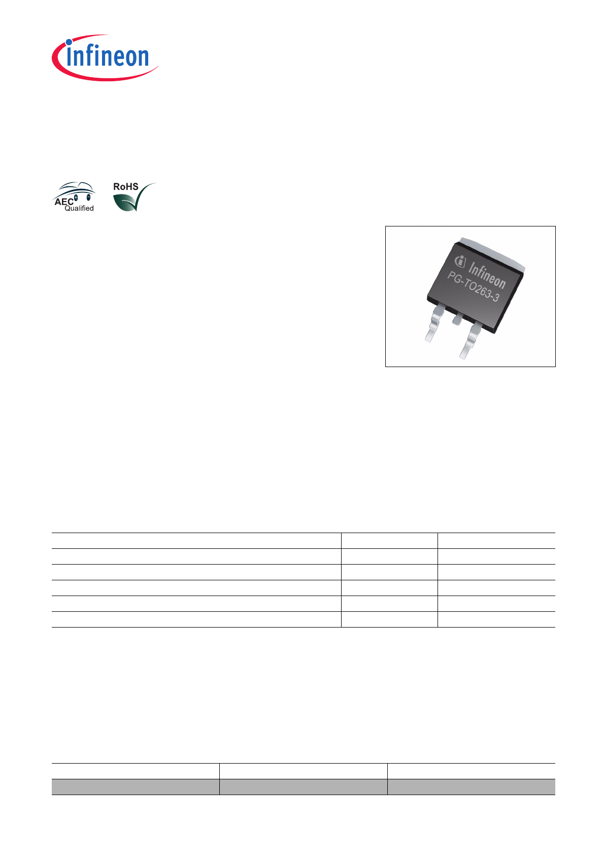
2
Block Diagram
Figure 1
Block Diagram
2.1
Terms
Figure 2
shows all external terms used in this data sheet.
Figure 2
Naming of electrical parameters
Drain
Source
IN
Over-
voltage
Protection
Gate
Driving
Unit
ESD
Protection
Over-
temperature
Protection
Over-
current
limitation
BlockDiagram.emf
V
BAT
GND
Terms.emf
IN
V
BAT
V
IN
I
IN
R
IN
Source
I
Source
Z
L
I
L,
I
D
V
OUT,
V
DS
Drain
Datasheet
6
Rev. 1.0, 2015-02-11
HITFET - BTS3018TC
Smart low side power switch
Pin Configuration
3
Pin Configuration
3.1
Pin Assignment BTS3018TC
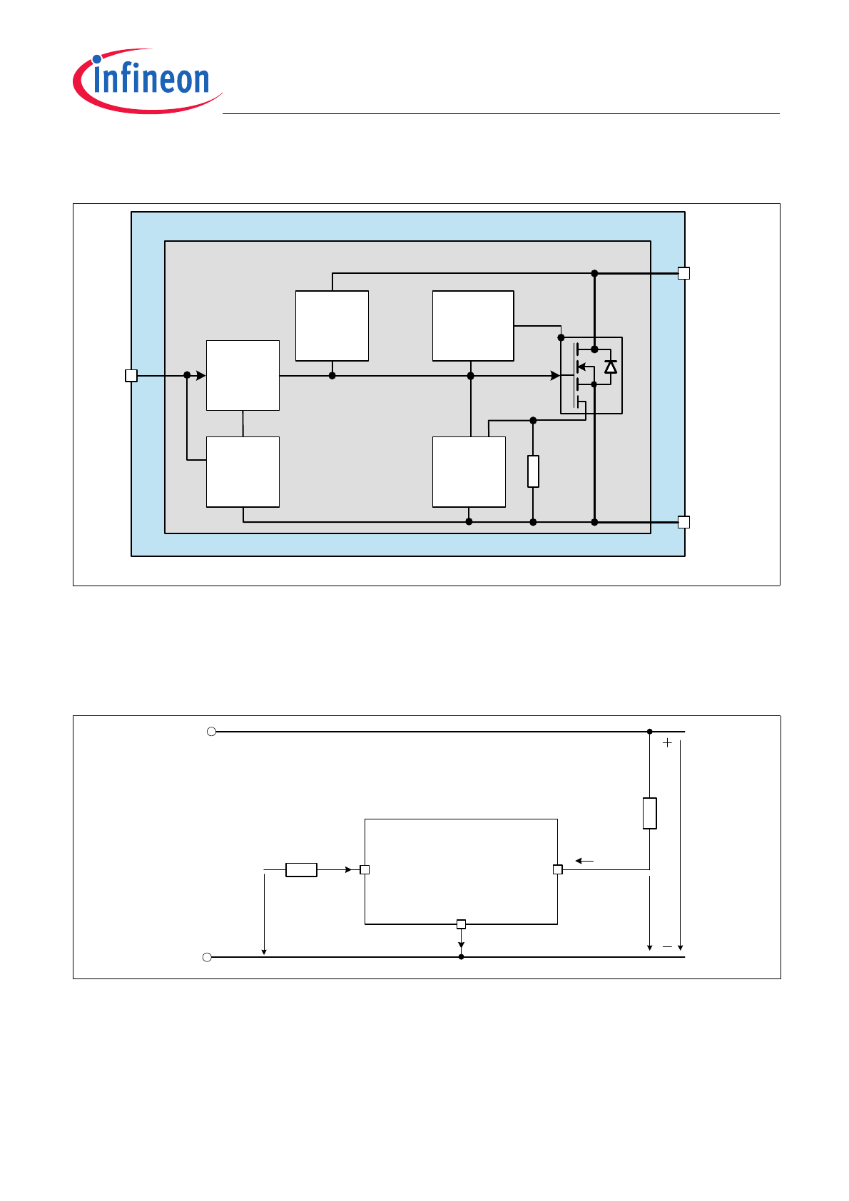
Figure 3
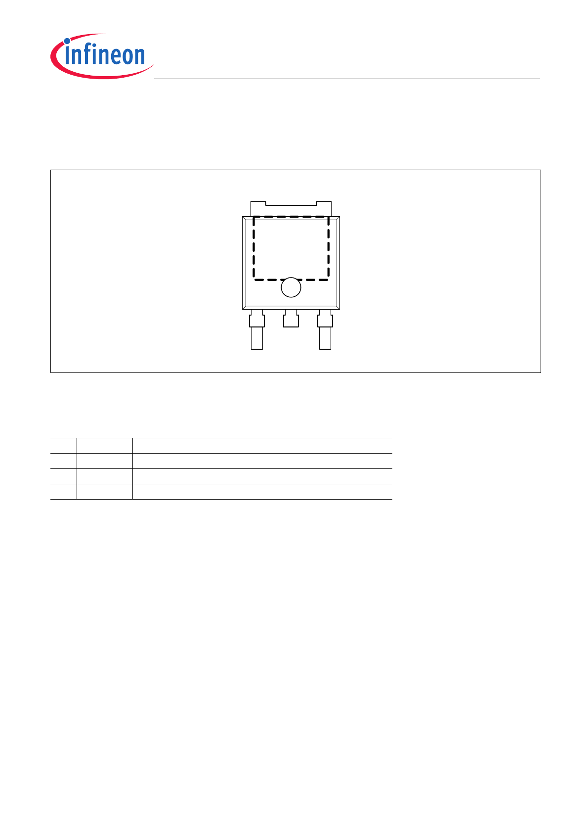
Pin Configuration PG-TO263-3-2
3.2
Pin Definitions and Functions
Table 2
Pin definition and functions
(top view )
4 (Tab)
1
3
2
Drain
Pin
Symbol
Function
1
IN
Input and fault feedback
2,4
Drain
Load connection for power DMOS
3
Source
Ground, Source of power DMOS

HITFET - BTS3018TC
Smart low side power switch
General Product Characteristics
Datasheet
7
Rev. 1.0, 2015-02-11
4
General Product Characteristics
4.1
Absolute Maximum Ratings
Note: Stresses above the ones listed here may cause permanent damage to the device. Exposure to absolute
maximum rating conditions for extended periods may affect device reliability.
Note: Integrated protection functions are designed to prevent IC destruction under fault conditions described in the
data sheet. Fault conditions are considered as “outside” normal operating range. Protection functions are
not designed for continuous repetitive operation
Absolute Maximum Ratings
1)
T
J
= -40
°C to +150 °C; all voltages with respect to ground, positive current flowing into pin
(unless otherwise specified)
Table 3
Absolute maximum ratings
1) Not subject to production test, specified by design.
Pos.
Parameter
Symbol Limit Values Unit
Test Conditions
Min.
Max.
Voltages
4.1.1
Output voltage
V
OUT
–
60
V
2)
V
IN
= 0 V,
I
L
= 10 mA
2) Active clamped.
4.1.2
Output voltage for short circuit protection
V
OUT(SC)
–
36
V
V
IN
= 5 V
4.1.3
Input Current
I
IN
self limited
mA
-0.2 V <
V
IN
< 10 V
-2
2
mA
V
IN
< -0.2 V
or
V
IN
> 10 V
4.1.4
Load Current
I
L
–
30
A
3)
3) Active limited
Energies
4.1.5
Unclamped single pulse inductive energy
single pulse
E
AS
–
1.9
J
I
L(0)
=
7.0A
V
BAT
= 28 V;
T
J(0)
= 150
°C
Temperatures
4.1.6
Operating temperature
T
J
-40
+150
°C
–
4.1.7
Storage temperature
T
STG
-55
+150
°C
–
ESD Susceptibility
4.1.8
ESD Resistivity
V
ESD
-2
2
kV
HBM
4)
4) ESD susceptibility, “JEDEC HBM” according to ANSI/ESDA/JEDEC JS001

Datasheet
8
Rev. 1.0, 2015-02-11
HITFET - BTS3018TC
Smart low side power switch
General Product Characteristics
4.2
Functional Range
Table 4
Functional range
Note: Within the functional range the IC operates as described in the circuit description. The electrical
characteristics are specified within the conditions given in the related electrical characteristics table.
4.3
Thermal Resistance
Note: This thermal data was generated in accordance with JEDEC JESD51 standards.
For more information, go to
www.jedec.org
.
Table 5
Thermal resistance
Pos.
Parameter
Symbol
Limit Values
Unit
Conditions
Min.
Max.
4.2.1
Input pin voltage (device ON)
V
IN
2
10
V
–
4.2.2
Output voltage
V
OUT
2.5
36
V
–
4.2.3
Input pin current consumption
I
IN(NOR)
–
30
µA
normal operation
4.2.4
Input pin feedback current
I
IN(FAULT)
–
1400
µA
fault indication
Pos.
Parameter
Symbol
Limit Values
Unit
Conditions
Min.
Typ.
Max.
4.3.5
Junction to Case
R
thJC
–
–
0.7
K/W
1)
2)
4.3.6
Junction to Ambient (2s2p)
R
thJA(2s2p)
–
25
–
K/W
1)
3)
4.3.7
Junction to Ambient
(1s0p+600mm
2
Cu)
R
thJA(1s0p)
–
45
–
K/W
1)
4)
1) Not subject to production test, specified by design
2) Specified
R
thJC
value is simulated at natural convection on a cold plate setup (all pins are fixed to ambient temperature).
T
a
= 25
°C. Device is loaded with 1W power.
3) Specified
R
thJA
value is according to Jedec JESD51-2,-7 at natural convection on FR4 2s2p board;
The product (Chip+Package) was simulated on a 76.2 x 114.3 x 1.5 mm board with 2 inner copper layers
(2 x 70
μm Cu, 2 x 35 μm Cu).
T
a
= 25
°C, Device is loaded with 1W power.
4) Specified
R
thJA
value is according to Jedec JESD51-2,-3 at natural convection on FR4 1s0p board;
The product (Chip+Package) was simulated on a 76.2 x 114.3 x 1.5 mm board with additional heatspreading copper area
of 600mm
2
and 70
μm thickness.
T
a
= 25
°C, Device is loaded with 1W power.
HITFET - BTS3018TC
Smart low side power switch
General Product Characteristics
Datasheet
9
Rev. 1.0, 2015-02-11
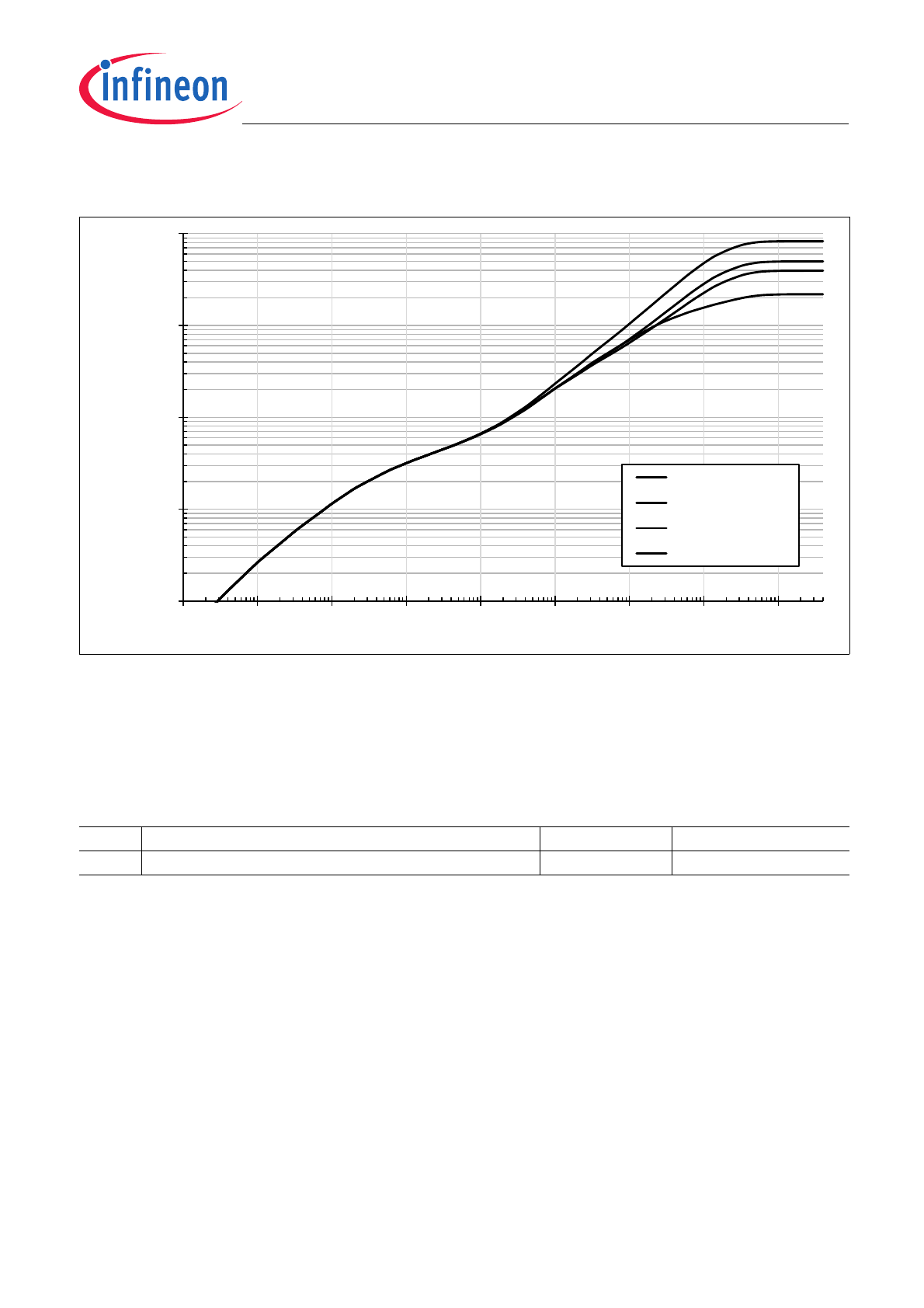
4.3.1
Transient Thermal Impedance
Figure 4
Typical transient thermal impedance Z
thJA
= f(t
p
) , T
a
= 25 °C
Value is according to Jedec JESD51-3,-5,-7 at natural convection on FR4 2s2p board;
4.4
Package
Table 6
.Package
0,01
0,10
1,00
10,00
100,00
0,00001
0,0001
0,001
0,01
0,1
1
10
100
1000
Z
thJ
A
[K/W]
time [sec]
(I) 1s0p-footprint
(II) 1s0p-300mm²
(III) 1s0p-600mm²
(IV) 2s2p
(I)
(II)
(III)
(IV)
Pos.
Parameter
Value
Test Conditions
4.4.1
Moisture Sensitivity Level
JESD20-D1
MSL1
–
Datasheet
10
Rev. 1.0, 2015-02-11
HITFET - BTS3018TC
Smart low side power switch
Input and Power Stage
5
Input and Power Stage
5.1
Input Circuit
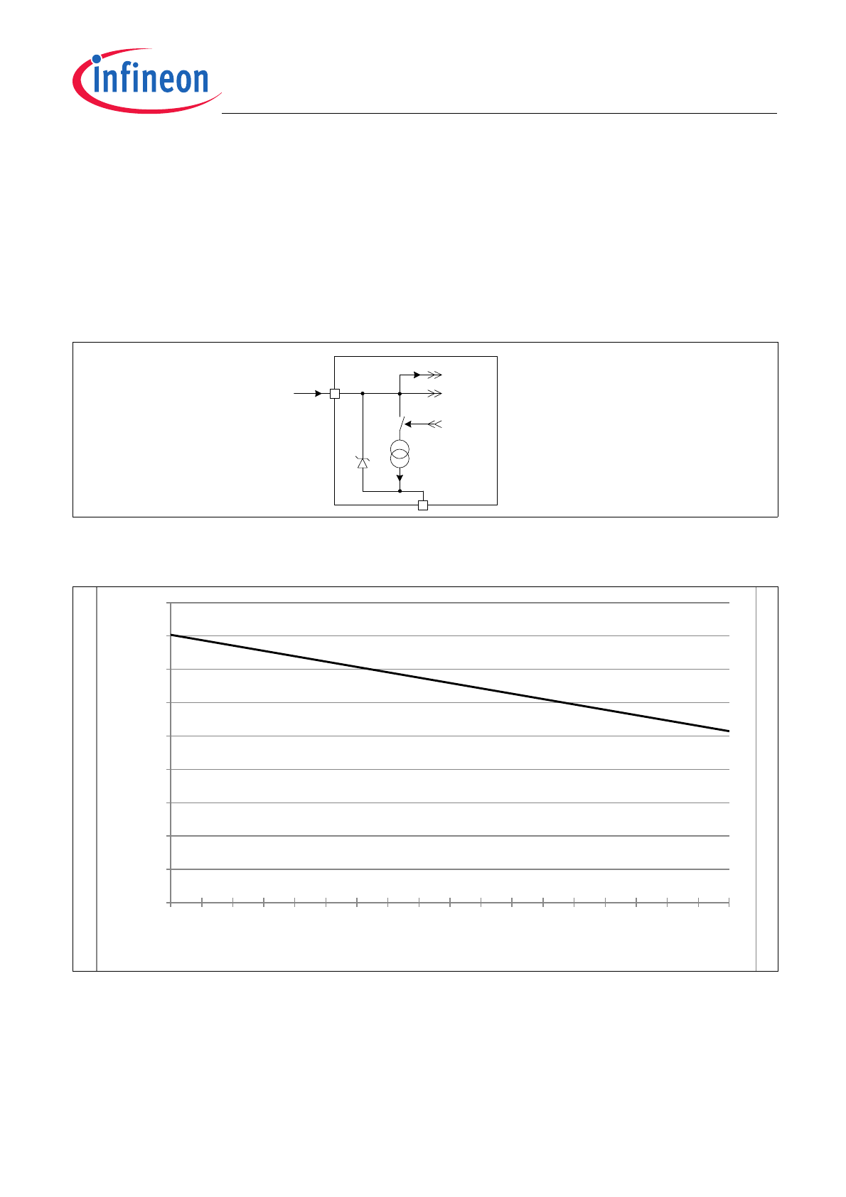
Figure 5
shows the input circuit of the BTS3018TC. The Zener Diode Z
D
protects the input circuit against ESD
pulses. The internal circuitry is powered via the input pin. During normal operation the Input is connected to the
Gate of the power MOSFET. During fault condition the device sinks the current
I
IN(FAULT)
to give the fault
information back to the driving circuit. The current handling capability of the driving circuit does not influence the
device behavior as long as the supply current
I
IN
is supplied.
Figure 5
Input Circuit
Figure 6
shows the typical input threshold voltage of the BTS3018TC.
Figure 6
Typical Input Threshold Voltage
V
IN(TH)
= f(
T
J
);
I
L
= 4.8mA ,
V
OUT
= 13.5V
Input .emf
Source
Z
D
IN
I
IN
Gate
Fault
condition
I
INf
I
IS
Logic
0
0,2
0,4
0,6
0,8
1
1,2
1,4
1,6
1,8
-40
-10
10
35
55
75
95
115
135
150
V
in(th)
[V]
Tj [°C]
V
IN(TH)
[V]