
Features
• Logic Level Input
• Input Protection (ESD)
•=Thermal shutdown with latch
• Overload protection
• Short circuit protection
• Overvoltage protection
•
Current limitation
• Status feedback with external input resistor
• Analog driving possible
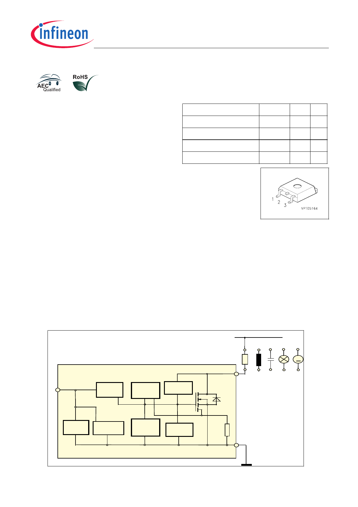
Product Summary
Drain source voltage
V
DS
60
V
On-state resistance
R
DS(on)
100 m
Ω
Current limit
I
D(lim)
7
A
Nominal load current
I
D(ISO)
3.5
A
Clamping energy
E
AS
1000 mJ
Application
• All kinds of resistive, inductive and capacitive loads in switching or
linear applications
• μC compatible power switch for 12 V and 24 V DC applications
• Replaces electromechanical relays and discrete circuits
General Description
N channel vertical power FET in Smart SIPMOS® chip on chip tech-
nology. Providing embedded protection functions.
p ro te c tio n
O v e rv o lta g e
D ra in
IN
E S D
H IT F E T
S o u rc e
C u rre n t
1
3
O v e r-
p ro te c tio n
te m p e ra tu re
S h o rt c irc u it
p ro te c tio n
+
d v /d t
lim ita tio n
lim ita tio n
V bb
S h o rt c irc u it
p ro te c tio n
L O A D
2
O v e rlo a d
p ro te c tio n
M
•
AEC qualified
• Green product (RoHS compliant)
Datasheet
1
Rev. 1.0, 2009-07-20
Smart Low Side Power Switch
HITFET BTS 117TC

Maximum Ratings at Tj = 25 °C unless otherwise specified
Parameter
Symbol
Value
Unit
Drain source voltage
V
DS
60
V
Drain source voltage for short circuit protection
V
DS(SC)
32
Continuous input current
1)
-0.2V
≤ V
IN
≤ 10V
V
IN
< -0.2V or
V
IN
> 10V
I
IN
no limit
|
I
IN
|
≤ 2
mA
Operating temperature
T
j
- 40 ... +150
°C
Storage temperature
T
stg
- 55 ... +150
Power dissipation
T
C
= 25 °C
P
tot
50
W
Unclamped single pulse inductive energy
I
D(ISO)
= 3.5 A
E
AS
1000
mJ
Electrostatic discharge voltage
(Human Body Model)
according to MIL STD 883D, method 3015.7 and
EOS/ESD assn. standard S5.1 - 1993
V
ESD
3000
V
Load dump protection
V
LoadDump
2)
=
V
A
+
V
S
V
IN
=low or high;
V
A
=13.5 V
t
d
= 400 ms,
R
I
= 2
Ω, I
D
=0,5*3.5A
t
d
= 400 ms,
R
I
= 2
Ω, I
D
= 3.5A
V
LD
75
70
Thermal resistance
junction - case:
R
thJC
2.5
K/W
junction - ambient:
R
thJA
75
SMD version, device on PCB:
3)
R
thJA
45
1In case of thermal shutdown a minimum sensor holding current of 500 μA has to be guaranteed (see also page 3).
2VLoaddump is setup without the DUT connected to the generator per ISO 7637-1 and DIN 40839
3 Device on 50mm*50mm*1.5mm epoxy PCB FR4 with 6cm 2 (one layer, 70μm thick) copper area for Drain connection.
PCB mounted vertical without blown air.
Datasheet
2
Rev. 1.0, 2009-07-20
Smart Low Side Power Switch
HITFET BTS 117TC

Electrical Characteristics
Parameter
Symbol
Values
Unit
at T
j
=25°C, unless otherwise specified
min.
typ.
max.
Characteristics
Drain source clamp voltage
T
j
= - 40 ...+ 150°C,
I
D
= 10 mA
V
DS(AZ)
60
-
73
V
Off state drain current
V
DS
= 32 V,
T
j
= -40...+150 °C,
V
IN
= 0 V
I
DSS
-
-
5
μA
Input threshold voltage
I
D
= 0.7 mA
V
IN(th)
1.3
1.7
2.2
V
Input current - normal operation,
I
D
<I
D(lim)
:
V
IN
= 10 V
I
IN(1)
-
30
60
μA
Input current - current limitation mode,
I
D
=
I
D(lim)
:
V
IN
= 10 V
I
IN(2)
-
120
300
Input current - after thermal shutdown,
I
D
=0 A:
V
IN
= 10 V
I
IN(3)
800
2200
4000
Input holding current after thermal shutdown
1)
T
j
= 25 °C
T
j
= 150 °C
I
IN(H)
500
300
-
-
-
-
On-state resistance
V
IN
= 5 V,
I
D
= 3.5 A,
T
j
= 25 °C
V
IN
= 5 V,
I
D
= 3.5 A,
T
j
= 150 °C
R
DS(on)
-
-
90
180
120
240
m
Ω
On-state resistance
V
IN
= 10 V,
I
D
= 3.5 A,
T
j
= 25 °C
V
IN
= 10 V,
I
D
= 3.5 A,
T
j
= 150 °C
R
DS(on)
-
-
80
160
100
200
Nominal load current (ISO 10483)
V
IN
= 10 V,
V
DS
= 0.5 V,
T
C
= 85 °C
I
D(ISO)
3.5
-
-
A
1If the input current is limited by external components, low drain currents can flow and heat the device.
Auto restart behaviour can occur.
Datasheet
3
Rev. 1.0, 2009-07-20
Smart Low Side Power Switch
HITFET BTS 117TC

Electrical Characteristics
Parameter
Symbol
Values
Unit
at T
j
=25°C, unless otherwise specified
min.
typ.
max.
Characteristics
Initial peak short circuit current limit
V
IN
= 10 V,
V
DS
= 12 V
I
D(SCp)
-
25
-
A
Current limit
1)
V
IN
= 10 V,
V
DS
= 12 V,
t
m
= 350 μs,
T
j
= -40...+150 °C
I
D(lim)
7
10
15
Dynamic Characteristics
Turn-on time
V
IN
to 90%
I
D
:
R
L
= 4.7
Ω, V
IN
= 0 to 10 V,
V
bb
= 12 V
t
on
-
40
70
μs
Turn-off time
V
IN
to 10%
I
D
:
R
L
= 4.7
Ω, V
IN
= 10 to 0 V,
V
bb
= 12 V
t
off
-
70
150
Slew rate on 70 to 50%
V
bb
:
R
L
= 4.7
Ω, V
IN
= 0 to 10 V,
V
bb
= 12 V
-dV
DS
/dt
on
-
1
3
V/μs
Slew rate off 50 to 70%
V
bb
:
R
L
= 4.7
Ω, V
IN
= 10 to 0 V,
V
bb
= 12 V
dV
DS
/dt
off
-
1
3
Protection Functions
Thermal overload trip temperature
T
jt
150
165
-
°C
Unclamped single pulse inductive energy
I
D
= 3.5 A,
T
j
= 25 °C,
V
bb
= 32 V
I
D
= 3.5 A,
T
j
= 150 °C,
V
bb
= 32 V
E
AS
1000
225
--
--
--
--
mJ
Inverse Diode
Inverse diode forward voltage
I
F
= 5*3.5A,
t
m
= 300
μS, V
IN
= 0 V
V
SD
-
1
-
V
2
)
1Device switched on into existing short circuit (see diagram Determination of I D(lim)). If the device is in on condition
and a short circuit occurs, these values might be exceeded for max. 50 μs.
2Integrated protection functions are designed to prevent IC destruction under fault conditions
described in the data sheet. Fault conditions are considered as "outside" normal operating range.
Protection functions are not designed for continuous repetitive operation.
Datasheet
4
Rev. 1.0, 2009-07-20
Smart Low Side Power Switch
HITFET BTS 117TC
Block Diagramm
Terms
Inductive and overvoltage output clamp
HITFET
IN
D
VIN
ID
VDS
1
IIN
S
Vbb
RL
2
3
HITFET
V
Z
D
S
Short circuit behaviour
V IN
I D
I D(SCp)
t 0
tm
t 2
I D(Lim)
t 1
Input circuit (ESD protection)
IN
ESD-ZD
I
Source
ESD zener diodes are not designed
for DC current > 2 mA @
V
IN
>10V.
t0: Turn on into a short circuit
tm: Measurementpoint for ID(lim)
t1: Activation of the fast temperature sensor and
regulation of the drain current to a level where
the junction temperature remains constant.
t2: Thermal shutdown caused by the second
temperature sensor, achieved by an
integrating measurement.
Datasheet
5
Rev. 1.0, 2009-07-20
Smart Low Side Power Switch
HITFET BTS 117TC
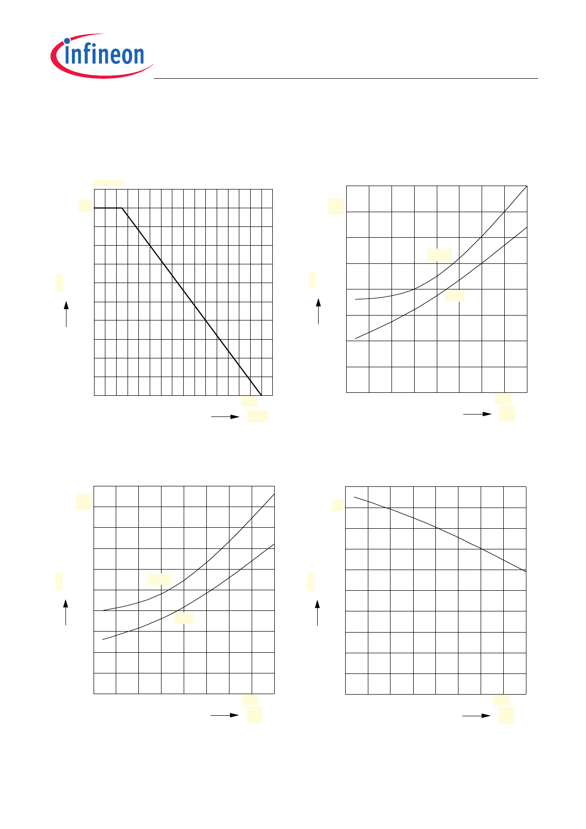
On-state resistance
R
ON
= f(T
j
); I
D
=3.5A; V
IN
=10V
-50
-25
0
25
50
75
100
°C
150
T
j
0
25
50
75
100
125
150
Ω
200
R
DS(on)
typ.
max.
Maximum allowable power dissipation
P
tot
= f(T
c
)
0
20
40
60
80
100
120
°C
160
150
0
5
10
15
20
25
30
35
40
45
W
55
BTS 117
P
tot
On-state resistance
R
ON
= f(T
j
); I
D
= 3.5A; V
IN
=5V
-50
-25
0
25
50
75
100
°C
150
T
j
0
25
50
75
100
125
150
175
200
Ω
250
R
DS(on)
typ.
max.
Typ. input threshold voltage
V
IN(th)
= f(T
j
); I
D
=0.7mA; V
DS
=12V
-50
-25
0
25
50
75
100
°C
150
T
j
0.0
0.2
0.4
0.6
0.8
1.0
1.2
1.4
1.6
V
2.0
V
IN(th)
Datasheet
6
Rev. 1.0, 2009-07-20
Smart Low Side Power Switch
HITFET BTS 117TC
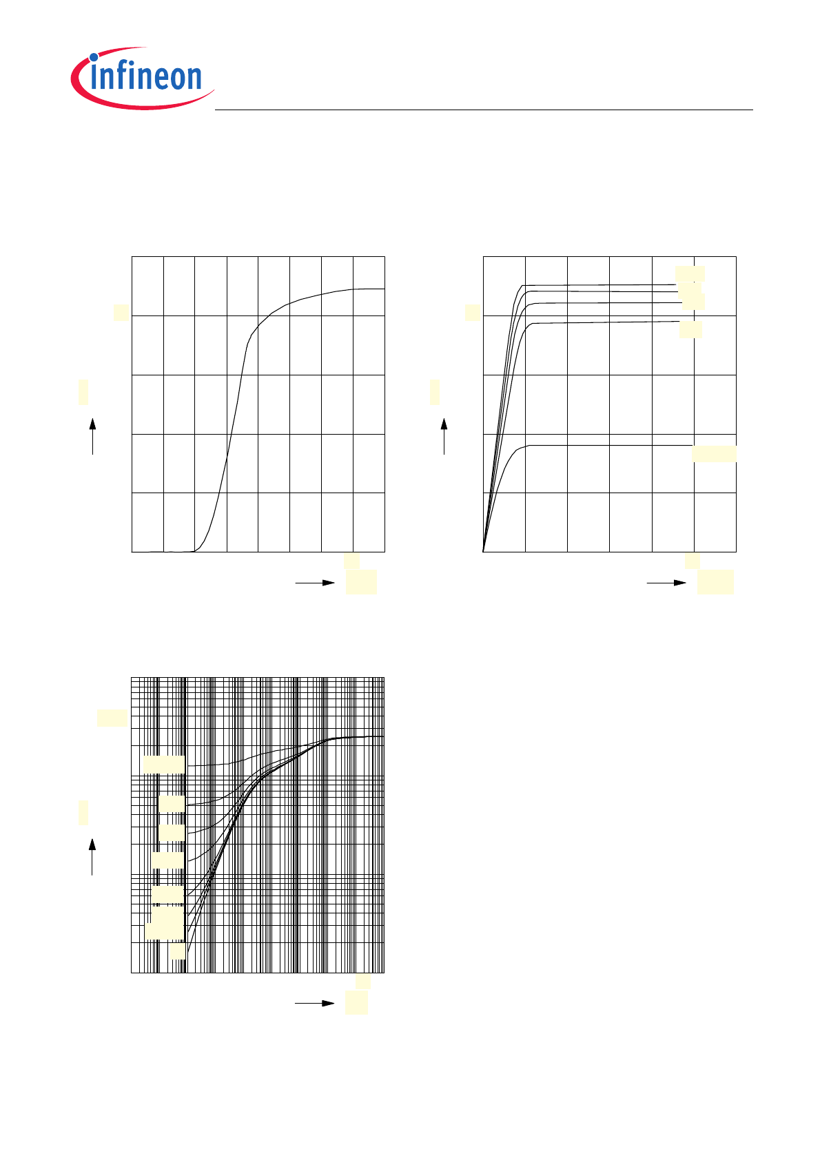
Typ. transfer characteristics
I
D
= f(V
IN
); V
DS
=12V; T
j
=25°C
0
1
2
3
4
5
6
V
8
V
IN
0
2
4
6
A
10
I
D
Typ. output characteristic
I
D
= f(V
DS
); T
j
=25°C
Parameter: V
IN
0
1
2
3
4
V
6
V
DS
0
2
4
6
A
10
I
D
Vin=3V
4V
5V
6V
10V
Transient thermal impedance
Z
thJC
=
f (t
p
)
parameter :
D = t
p
/
T
10
-7
10
-6
10
-5
10
-4
10
-3
10
-2
10
-1
10
0
10
2
s
t
P
-2
10
-1
10
0
10
1
10
K/W
R
thJC
0
0.005
0.01
0.02
0.05
0.1
0.2
D=0.5
Datasheet
7
Rev. 1.0, 2009-07-20
Smart Low Side Power Switch
HITFET BTS 117TC
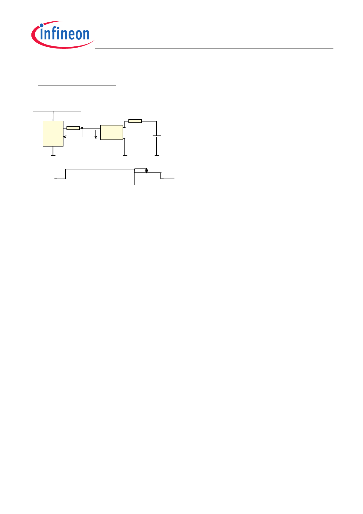
Application examples:
Status signal of thermal shutdown by
monitoring input current
D
S
IN
μC
V
bb
HITFET
V
IN
RSt
V
IN
thermal shutdown
Δ V
μC
ΔV = R
ST
*
I
IN(3)
Datasheet
8
Rev. 1.0, 2009-07-20
Smart Low Side Power Switch
HITFET BTS 117TC
Datasheet
9
Rev. 1.0, 2009-07-20
Smart Low Side Power Switch
HITFET BTS 117TC
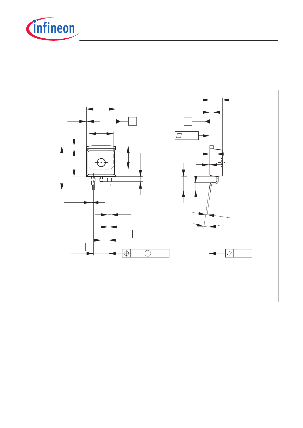
Package Outlines
1
Package Outlines
MAX.
B
A
0.25
M
±0.2
GPT09085
10
8.5
1)
7.55
1)
(15)
±0.2
9.25
±0.3
1
0...0.15
5.08
2.54
0.75
±0.1
1.05
±0.1
1.27
4.4
B
0.5
±0.1
±0.3
2.7
4.7
±0.5
±0.3
1.3
2.4
0...0.3
A
All metal surfaces tin plated, except area of cut.
Metal surface min. X = 7.25, Y = 6.9
Typical
1)
0.1 B
0.1
0.05
8˚
Figure 1
PG-TO263-3-2 (Plastic Dual Small Outline Package) (RoHS-Compliant)
To meet the world-wide customer requirements for environmentally friendly products and to be compliant with
government regulations the device is available as a green product. Green products are RoHS-Compliant (i.e Pb-
free finish on leads and suitable for Pb-free soldering according to IPC/JEDEC J-STD-020).
Please specify the package needed (e.g. green package) when placing an order
You can find all of our packages, sorts of packing and others in our
Infineon Internet Page “Products”:
http://www.infineon.com/products
.
Dimensions in mm

Datasheet
10
Rev. 1.0, 2009-07-20
Smart Low Side Power Switch
HITFET BTS 117TC
Revision History
2
Revision History
Version
Date
Changes
Rev. 1.0
2009-07-20
intial released Datasheet