

BTS4130QGA
Smart High-Side Power Switch
Data Sheet, Rev. 1.0, March 2008
Automotive Power

Datasheet
2
1.0, 2008-27-02
BTS 4130QGA
1
Overview 3
2
Block Diagram 5
3
Pin Configuration 6
3.1
Pin Assignment 6
3.2
Pin Definitions and Functions 6
3.3
Voltage and Current Definition 7
4
General Product Characteristics 8
4.1
Absolute Maximum Ratings 8
4.2
Functional Range 9
4.3
Thermal Resistance 9
5
Power Stage 10
5.1
Output ON-State Resistance 10
5.2
Turn ON / OFF Characteristics 10
5.3
Inductive Output Clamp 11
5.3.1
Maximum Load Inductance 12
5.4
Electrical Characteristics Power Stage 13
6
Protection Mechanisms 14
6.1
Loss of Ground Protection 14
6.2
Undervoltage Protection 14
6.3
Overvoltage Protection 14
6.4
Reverse Polarity Protection 15
6.5
Overload Protection 15
6.5.1
Current Limitation 16
6.6
Electrical Characteristics Protection Functions 17
7
Diagnostic Mechanism 18
7.1
ST 0/1/2/3 Pin 18
7.2
ST0/1/2/3 Signal in Case of Failures 18
7.2.1
Diagnostic in Open Load, Channel OFF 19
7.2.2
ST 0/1 Signal in case of Over Temperature 20
7.3
Electrical Characteristics Diagnostic Functions 21
8
Input Pins 22
8.1
Input Circuitry 22
8.2
Electrical Characteristics 22
9
Application Information 23
9.1
Further Application Information 23
10
Package Outlines 24
11
Revision History 25
PG-DSO-20-32
Type
Package
Marking
BTS4130QGA
PG-DSO-20-32
BTS4130QGA
Data Sheet
3
Rev. 1.0, 2008-03-18
Smart High-Side Power Switch
Four Channel Device
BTS4130QGA
1
Overview
Basic Features
•
Withstand low Cranking Voltage
•
Fit for 12V Application
•
Four Channel device
•
Very low Stand-by Current
•
CMOS Compatible Inputs
•
Electrostatic Discharge Protection (ESD)
•
Optimized Electromagnetic Compatibility
•
Logic ground independent from load ground
•
Very low Leakage Current from OUT to the load in OFF State
•
Green Product (RoHS compliant)
•
AEC Qualified
Description
The BTS4130QGA is a quad channel Smart High-Side Power Switch. It is embedded in a PG-DSO-20-32
package, providing protective functions and diagnostics. The power transistor is built by a N-channel power
MOSFET with charge pump. The device is monolithically integrated in Smart technology. It is specially designed
to drive relays as well as resistive loads in the harsh automotive environment.
Table 1
Electrical Parameters (short form)
Parameter
Symbol
Value
Operating voltage range
V
SOP
5.5V .... 20V
Undervoltage switch OFF at
T
j
= -40°C
V
s (USO)
3.2V
Maximum load per channel
P
BULB
2 * R5W, relays or LED
Over voltage protection
V
S (AZ)
43V
Max ON State resistance at
T
j
= 150°C per channel
R
DS(ON)
260m
Ω
Nominal load current (one channel active)
I
L (nom)
1.8A
Minimum current limitation
I
L_SCR
5A
Standby current for the whole device with load
I
S(off)
16µA
Maximum reverse battery voltage
-
V
s(REV)
32V

Data Sheet
4
Rev. 1.0, 2008-03-18
BTS4130QGA
Overview
Diagnostic Feature
•
Open load detection in OFF state
•
Feedback of the thermal shutdown in ON state
•
Diagnostic feedback with open drain output
Protection Functions
•
Short circuit protection
•
Overload protection
•
Current limitation
•
Thermal shutdown
•
Overvoltage protection (including load dump) with external resistor
•
Reverse battery protection with external resistor
•
Loss of ground and loss of
V
S
protection
•
Electrostatic discharge protection (ESD)
Application
•
All types of resistiv, inductive and capacitive loads
Data Sheet
5
Rev. 1.0, 2008-03-18
BTS4130QGA
Block Diagram
2
Block Diagram
Figure 1
Block diagram for the BTS4130QGA
Block diagram .emf
Channel 0
V
S
OUT 0
IN0
T
driver
logic
gate control
&
charge pump
open load detection
over
temperature
clamp for
inductive load
over current
switch off
voltage sensor
ESD
protection
ST 0/1
internal
power
supply
Channel 1
IN1
Control and protection circuit equivalent to channel 0
T
V
S
OUT 1
Channel 2
V
S
OUT 2
IN2
T
driver
logic
gate control
&
charge pump
open load detection
over
temperature
clamp for
inductive load
over current
switch off
voltage sensor
GND
ESD
protection
ST 2/3
internal
power
supply
Channel 3
IN3
Control and protection circuit equivalent to channel 0
T
V
S
OUT 3
Data Sheet
6
Rev. 1.0, 2008-03-18
BTS4130QGA
Pin Configuration
3
Pin Configuration
3.1
Pin Assignment
Figure 2
Pin Configuration
3.2
Pin Definitions and Functions
Pin
Symbol
Function
1, 10, 11,
12, 15, 16,
19, 20
V
S
Battery voltage; Design the wiring for the simultaneous maximum short circuit
currents from channel 0 and 1 and also for low thermal resistance
2
GND0/1
Ground; Ground connection for channel 0 and 1
3
IN0
Input channel 0; Input signal for channel 0. Activate the channel in case of logic
high level
4
ST 0/1
Diagnostic feedback; of channel 0/1. Open drain.
5
IN1
Input channel 1; Input signal for channel 1. Activate the channel in case of logic
high level
6
GND2/3
Ground; Ground connection for channel 2 and 3
7
IN2
Input channel 2; Input signal for channel 2. Activate the channel in case of logic
high level
8
ST 2/3
Diagnostic feedback; of channel 2/3. Open drain.
9
IN3
Input channel 3; Input signal for channel 3. Activate the channel in case of logic
high level
1
2
3
4
14
13
12
11
ST 0/1
GND0/1
IN0
Vs
5
6
7
IN1
17
16
15
OUT0
OUT1
Vs
GND2/3
Pinout SO20 shared diag.vsd
10
9
8
20
19
18
Vs
Vs
Vs
OUT3
OUT2
Vs
Vs
Vs
IN2
ST2/3
IN3
Data Sheet
7
Rev. 1.0, 2008-03-18
BTS4130QGA
Pin Configuration
3.3
Voltage and Current Definition
Figure 3
shows all terms used in this data sheet, with associated convention for positive values.
Figure 3
Voltage and current definition
13
OUT3
Output 3; Protected High side power output channel 3
14
OUT2
Output 2; Protected High side power output channel 2
17
OUT1
Output 1; Protected High side power output channel 1
18
OUT0
Output 0; Protected High side power output channel 0
Pin
Symbol
Function
V
S
IN0
IN1
ST 0/1
GND
OUT0
OUT1
I
IN 0
I
IN1
I
ST0/1
V
S
V
IN0
V
IN1
V
ST0 /1
I
S
I
GND
V
D S0
V
DS1
V
OUT0
V
OUT1
Voltage and current convention quad
shared diag.vsd
IN2
IN3
ST 2/3
I
IN 2
I
IN 3
I
ST2/3
OUT2
OUT3
V
OU T3
V
D S2
V
DS3
V
OUT2
I
OUT3
I
OU T0
I
OUT1
I
OU T2

Data Sheet
8
Rev. 1.0, 2008-03-18
BTS4130QGA
General Product Characteristics
4
General Product Characteristics
4.1
Absolute Maximum Ratings
Note: Stresses above the ones listed here may cause permanent damage to the device. Exposure to absolute
maximum rating conditions for extended periods may affect device reliability.
Absolute Maximum Ratings
1)
T
J
= 25°C; (unless otherwise specified)
1) Not subject to production test, specified by design
Pos.
Parameter
Symbol
Limit values
Unit
Conditions
Min.
Max.
Voltages
4.1.1
Supply voltage
V
S
-0.3
43
V
–
4.1.2
Reverse polarity Voltage
-
V
S(REV)
–
32
V
–
4.1.3
Supply voltage for short circuit protection
V
bat(SC)
0
20
V
R
ECU
= 20m
Ω,
R
Cable
= 16m
Ω
/m,
L
Cable
= 1µH/m,
l
= 0 or 5m
2)
see
Chapter 6
2) Set up in accordance to AEC Q100-012 and AEC Q101-006
Input pins
4.1.4
Voltage at INPUT pins
V
IN
-10
16
V
–
4.1.5
Current through INPUT pins
I
IN
-0.3
0.3
mA
–
4.1.6
Current through INPUT pins pulsed
I
IN
-5
5
mA
Only for testing
Status pin
4.1.7
Current through ST 0/1 pin
I
ST0/1
-5
5
mA
–
4.1.8
Current through ST 2/3 pin
I
ST2/3
-5
5
mA
–
Power stage
4.1.9
Load current
|
I
L
|
–
I
L(LIM)
A
–
4.1.10
Power dissipation (DC), all channel
active
P
TOT
–
1.4
W
T
A
= 85°C,
T
j
<150°C
4.1.11
Maximum Switchable energy, single
pulse
E
AS
–
76
mJ
I
L
= 2.3A,
V
S
= 12V
Temperatures
4.1.12
Junction Temperature
T
j
-40
150
°
C
–
4.1.13
Dynamic temperature increase while
switching
∆
T
j
–
60
K
–
4.1.14
Storage Temperature
T
stg
-55
150
°
C
–
ESD Susceptibility
4.1.15
ESD Resistivity IN pin
V
ESD
-1
1
kV
HBM
3)
3) ESD susceptibility HBM according to EIA/JESD 22-A 114B
4.1.16
ESD Resistivity ST 0/1, 2/3 pins
V
ESD
-4
4
kV
HBM
3)
4.1.17
ESD Resistivity OUT to all other pins
shorted
V
ESD
-5
5
kV
HBM
3)

Data Sheet
9
Rev. 1.0, 2008-03-18
BTS4130QGA
General Product Characteristics
Note: Integrated protection functions are designed to prevent IC destruction under fault conditions described in the
data sheet. Fault conditions are considered as “outside” normal operating range. Protection functions are
not designed for continuous repetitive operation.
4.2
Functional Range
T
j
= -40
°
C to +150
°
C; (unless otherwise specified)
Note: Within the functional range the IC operates as described in the circuit description. The electrical
characteristics are specified within the conditions given in the related electrical characteristics table.
4.3
Thermal Resistance
Pos.
Parameter
Symbol
Limit values
Unit
Conditions
Min.
Max.
4.2.1
Operating Voltage
V
SOP
5.5
20
V
V
IN
= 4.5V,
R
L
= 12
Ω,
V
DS
< 0.5V
4.2.2
Undervoltage switch OFF
V
SUV
–
3.2
V
-
1)
,
T
j
= -40°C,
V
DS
< 0.5V
1) Battery voltage is decreasing
4.2.3
Operating current
One channel active
Four channels active
I
GND
–
–
0.9
3.3
mA
V
IN
= 5V
4.2.4
Standby current for whole device
with load
I
S(OFF)
–
–
–
16
16
24
µA
T
j
= 25°C
T
j
= 85°C
2)
T
j
= 150°C,
V
s
= 12V,
R
L
= 12
Ω,
V
IN
= 0V
2) Not subject to production test. Specified by design
Pos.
Parameter
Symbol
Limit values
Unit
Conditions
Min.
Typ.
Max.
4.3.1
Junction to Soldering Point each
channel
R
thJSP
–
–
15
K/W
–
1)
1) Not subject to production test, specified by design
4.3.2
Junction to Ambient
R
thJA
–
45
–
K/W
with 6cm² cooling
area
1)
Data Sheet
10
Rev. 1.0, 2008-03-18
BTS4130QGA
Power Stage
5
Power Stage
The power stages are built by an N-channel vertical power MOSFET (DMOS) with charge pump.
5.1
Output ON-State Resistance
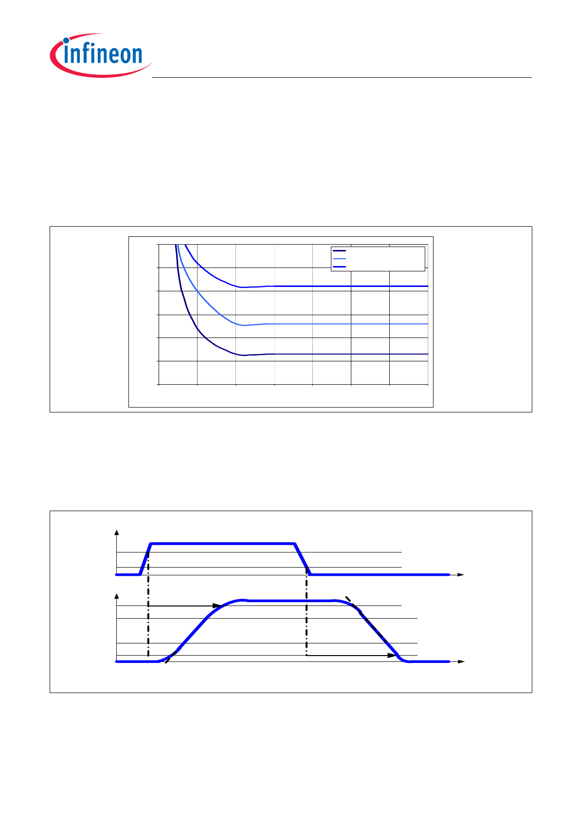
The ON-state resistance
R
DS(ON)
depends on the supply voltage as well as the junction temperature T
j
.
Figure 4
shows the dependencies for the typical ON-state resistance. The behavior in reverse polarity is described in
Chapter 6.4
.
Figure 4
Typical ON-state resistance
A high signal (See
Chapter 8
) at the input pin causes the power DMOS to switch ON with a dedicated slope, which
is optimized in terms of EMC emission.
5.2
Turn ON / OFF Characteristics
Figure 5
shows the typical timing when switching a resistive load.
Figure 5
Turn ON/OFF (resistive) timing
0
50
100
150
200
250
300
5
7
9
11
13
15
17
19
VS (V)
Rd
so
n
(
m
Oh
m
)
Rdson (mOhm) @ -40°C
Rdson (mOhm) @ +25°C
Rdson (mOhm) @ +150°C
ron.vsd
IN
t
V
OUT
t
ON
t
OFF
90% V
S
10% V
S
V
IN_H_min
V
IN_L_max
t
Switching times .vsd
30% V
S
70% V
S
dV/dt
ON
dV/dt
OFF