
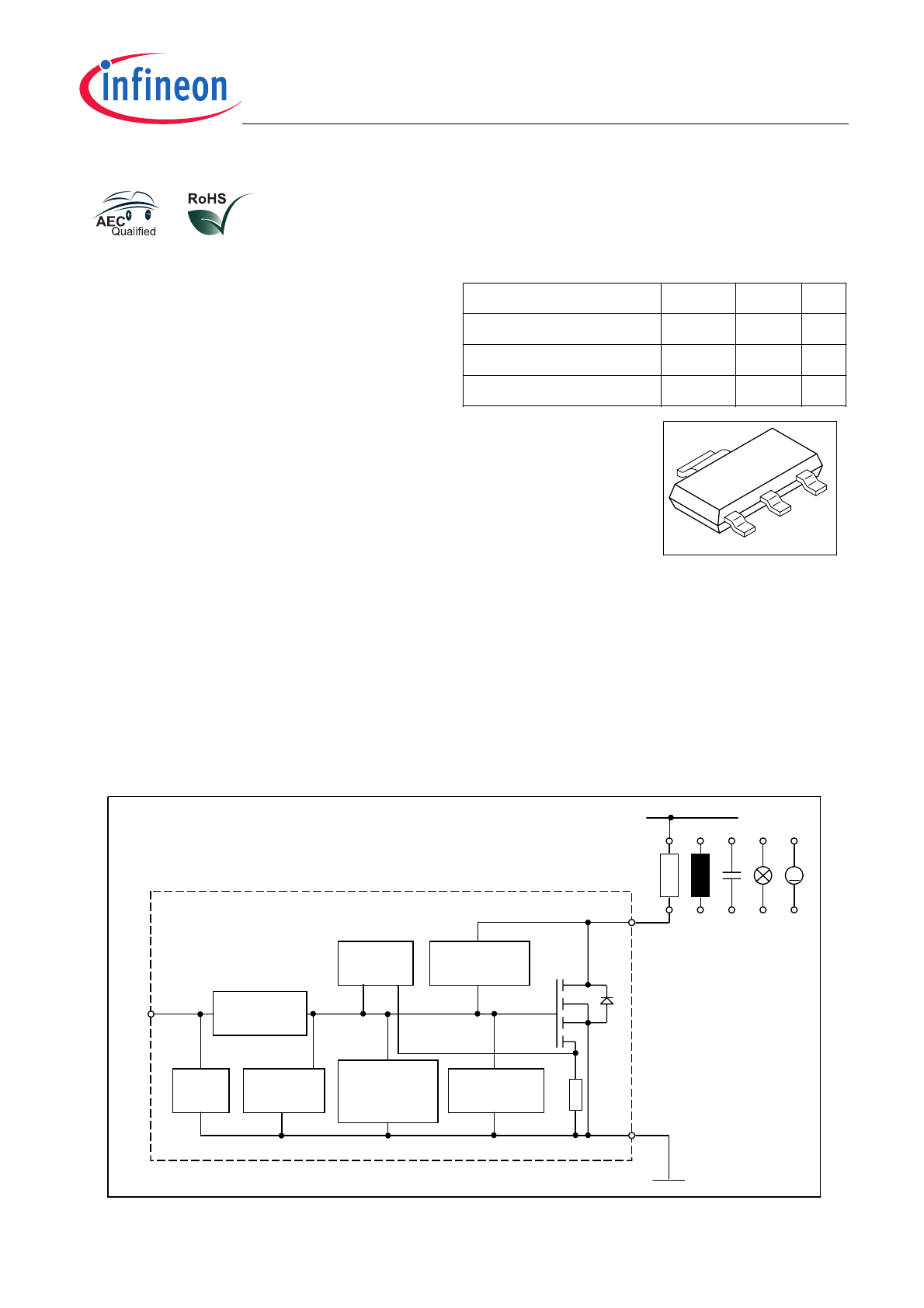
Product Summary
Drain source voltage
V
DS
42
V
On-state resistance
R
DS(on)
50
m
W
Nominal load current
I
D(Nom)
3
A
Clamping energy
E
AS
500
mJ
VPS05163
1
2
3
4
Application
· All kinds of resistive, inductive and capacitive loads in switching
or linear applications
· µC compatible power switch for 12 V DC applications
· Replaces electromechanical relays and discrete circuits
General Description
N channel vertical power FET in Smart SIPMOSÒ technology. Fully protected by embedded
protection functions.
Gate-Driving
Unit
ESD
Overload
Protection
Over-
temperature
Protection
Short circuit
Protection
Overvoltage-
Protection
Current
Limitation
M
V
bb
In
Source
Drain
HITFET
â
Pin 1
Pin 2 and 4 (TAB)
Pin 3
Complete product spectrum and additional information http://www.infineon.com/hitfet
Features
· Logic Level Input
· Input Protection (ESD)
· Thermal shutdown with auto restart
• Green product (RoHS compliant)
· Overload protection
· Short circuit protection
· Overvoltage protection
· Current limitation
· Analog driving possible
Datasheet
1
Rev. 1.3, 2008-04-14
Smart Low Side Power Switch
HITFET BSP 78

Maximum Ratings at T
j
= 25°C, unless otherwise specified
Parameter
Symbol
Value
Unit
Drain source voltage
V
DS
42
V
Supply voltage for full short circuit protection
V
bb(SC)
42
Continuous input voltage
1)
V
IN
-0.2
2)
... +10
Continuous input current
2)
-0.2V
£ V
IN
£ 10V
V
IN
< -0.2V or
V
IN
> 10V
I
IN
self limited
|
I
IN
|
£ 2
mA
Operating temperature
T
j
-40 ...+150
°C
Storage temperature
T
stg
-55 ... +150
Power dissipation
5)
T
C
= 85 °C
P
tot
3.8
W
Unclamped single pulse inductive energy
2)
E
AS
500
mJ
Load dump protection
V
LoadDump
2)3)
=
V
A
+
V
S
V
IN
= 0 and 10 V, t
d
= 400 ms,
R
I
= 2
W,
R
L
= 4.5
W, V
A
= 13.5 V
V
LD
53.5
V
V
ESD
2
kV
Thermal resistance
junction - ambient:
@ min. footprint
@ 6 cm
2
cooling area
4)
R
thJA
125
72
K/W
junction-soldering point:
R
thJS
17
K/W
1For input voltages beyond these limits I
IN
has to be limited.
2not subject to production test, specified by design
3VLoaddump is setup without the DUT connected to the generator per ISO 7637-1 and DIN 40839
4 Device on 50mm*50mm*1.5mm epoxy PCB FR4 with 6cm2 (one layer, 70µm thick) copper area for drain
connection. PCB mounted vertical without blown air.
5not subject to production test, calculated by R
thJA and Rds(on)
Electrostatic discharge voltage
2)
(Human Body Model)
according to
Jedec norm
EIA/JESD22-A114-B, Section 4
Datasheet
2
Rev. 1.3, 2008-04-14
Smart Low Side Power Switch
HITFET BSP 78

Electrical Characteristics
Parameter
Symbol
Values
Unit
at
T
j
= 25°C, unless otherwise specified
min.
typ.
max.
Characteristics
Drain source clamp voltage
T
j
= - 40 ...+ 150,
I
D
= 10 mA
V
DS(AZ)
42
-
55
V
Off-state drain current
T
j
= -40...+85 °C,
V
DS
= 32 V ,
V
IN
= 0 V
T
j
= 150 °C
I
DSS
-
-
1.5
5
8
15
µA
Input threshold voltage
I
D
=
1.4 mA, T
j
= 25 °C
I
D
=
1.4 mA, T
j
= 150 °C
V
IN(th)
1.3
0.8
1.7
-
2.2
-
V
On state input current
I
IN(on)
-
10
30
µA
On-state resistance
V
IN
= 5 V,
I
D
= 3 A,
T
j
= 25 °C
V
IN
= 5 V,
I
D
= 3 A,
T
j
= 150 °C
R
DS(on)
-
-
45
75
60
100
m
W
On-state resistance
V
IN
= 10 V,
I
D
= 3 A,
T
j
= 25 °C
V
IN
= 10 V,
I
D
= 3 A,
T
j
= 150 °C
R
DS(on)
-
-
35
65
50
90
Nominal load current
5)
V
DS
= 0.5 V,
T
j
< 150°C,
V
IN
= 10 V,
T
A
= 85 °C
I
D(Nom)
3
4
-
A
Current limit (active if
V
DS
>2.5 V)
1)
V
IN
= 10 V,
V
DS
= 12 V,
t
m
= 200 µs
I
D(lim)
18
24
30
1Device switched on into existing short circuit (see diagram Determination of ID(lim)). If the device is in on condit
and a short circuit occurs, these values might be exceeded for max. 50 µs.
5not subject to production test, calculated by R
thJA and Rds(on)
Datasheet
3
Rev. 1.3, 2008-04-14
Smart Low Side Power Switch
HITFET BSP 78

Electrical Characteristics
Parameter
Symbol
Values
Unit
at
T
j
= 25°C, unless otherwise specified
min.
typ.
max.
Dynamic Characteristics
Turn-on time
V
IN
to 90%
I
D
:
R
L
= 4.7
W, V
IN
= 0 to 10 V,
V
bb
= 12 V
t
on
-
60
100
µs
Turn-off time
V
IN
to 10%
I
D
:
R
L
= 4.7
W, V
IN
= 10 to 0 V,
V
bb
= 12 V
t
off
-
60
100
Slew rate on 70 to 50%
V
bb
:
R
L
= 4.7
W, V
IN
= 0 to 10 V,
V
bb
= 12 V
-dV
DS
/dt
on
-
0.3
1.5
V/µs
Slew rate off 50 to 70%
V
bb
:
R
L
= 4.7
W, V
IN
= 10 to 0 V,
V
bb
= 12 V
dV
DS
/dt
off
-
0.7
1.5
Protection Functions
1)
Thermal overload trip temperature
T
jt
150
175
-
°C
Thermal hysteresis
2)
DT
jt
-
10
-
K
Input current protection mode
T
j
= 150 °C
I
IN(Prot)
-
130
300
µA
Unclamped single pulse inductive energy
2)
I
D
= 3 A,
T
j
= 25 °C,
V
bb
= 12 V
E
AS
500
-
-
mJ
Inverse Diode
Inverse diode forward voltage
I
F
= 15 A,
t
m
= 250 µs,
V
IN
= 0 V,
t
P
= 300 µs
V
SD
-
1
1.5
V
1Integrated protection functions are designed to prevent IC destruction under fault conditions
described in the data sheet. Fault conditions are considered as "outside" normal operating range.
Protection functions are not designed for continuous repetitive operation.
2not subject to production test, specified by design
Datasheet
4
Rev. 1.3, 2008-04-14
Smart Low Side Power Switch
HITFET BSP 78
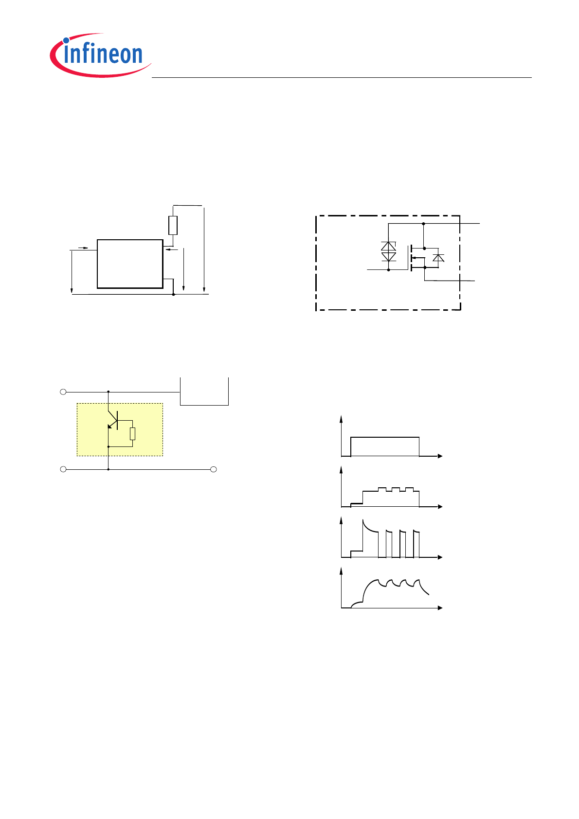
Block diagram
Inductive and overvoltage
output clamp
Terms
HITFET
IN
D
VIN
I D
VDS
1
IIN
S
Vbb
RL
2
3
HITFET
V
Z
D
S
Short circuit behaviour
Input circuit (ESD protection)
Gate Drive
Source/
Ground
Input
V
IN
I
IN
I
DS
T
j
Datasheet
5
Rev. 1.3, 2008-04-14
Smart Low Side Power Switch
HITFET BSP 78
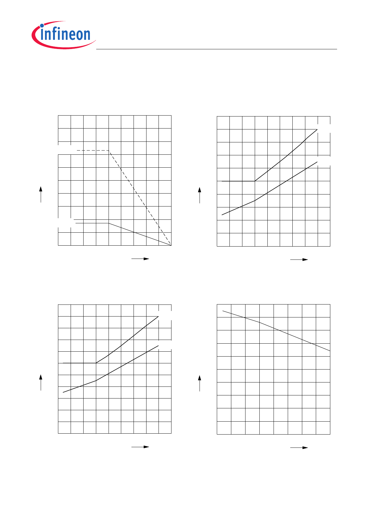
1 Maximum allowable power dissipation
P
tot
= f(T
S
) resp.
P
tot
= f(T
A
) @ R
thJA
=72 K/W
-75
-50
-25
0
25
50
75
100
°C
150
T
S
;
T
A
0
1
2
3
4
5
6
7
8
W
10
P
tot
6cm2
max.
2 On-state resistance
R
ON
= f(T
j
); I
D
=3A; V
IN
=10V
-50
-25
0
25
50
75
100
125
°C
175
T
j
0
10
20
30
40
50
60
70
80
m
W
100
R
DS(on)
typ.
max.
3 On-state resistance
R
ON
= f(T
j
); I
D
= 3A; V
IN
=5V
-50
-25
0
25
50
75
100
125
°C
175
T
j
0
10
20
30
40
50
60
70
80
90
m
W
110
R
DS(on)
typ.
max.
4 Typ. input threshold voltage
V
IN(th)
= f(T
j
);
I
D
= 0.7 mA; V
DS
= 12V
-50
-25
0
25
50
75
100
°C
150
T
j
0
0.2
0.4
0.6
0.8
1
1.2
1.4
1.6
V
2
V
GS(th)
Datasheet
6
Rev. 1.3, 2008-04-14
Smart Low Side Power Switch
HITFET BSP 78
5 Typ. transfer characteristics
I
D
=f(V
IN
); V
DS
=12V; T
Jstart
=25°C
0
1
2
3
4
5
6
7
8
V
10
V
IN
0
5
10
15
20
A
30
I
D
6 Typ. short circuit current
I
D(lim)
= f(T
j
); V
DS
=12V
Parameter: V
IN
-50
-25
0
25
50
75
100
125
°C
175
T
j
0
5
10
15
20
A
30
I
D
5V
Vin=10V
7 Typ. output characteristics
I
D
=f(V
DS
); T
Jstart
=25°C
Parameter: V
IN
0
1
2
3
4
V
6
V
DS
0
5
10
15
20
25
A
35
I
D
Vin=3V
4V
5V
6V
10V
7V
8 Off-state drain current
I
DSS
= f(
T
j
)
-40
-15
10
35
60
85
110
135
°C
185
T
j
0
2
4
6
8
10
12
µA
16
I
DSS
typ.
max.
Datasheet
7
Rev. 1.3, 2008-04-14
Smart Low Side Power Switch
HITFET BSP 78
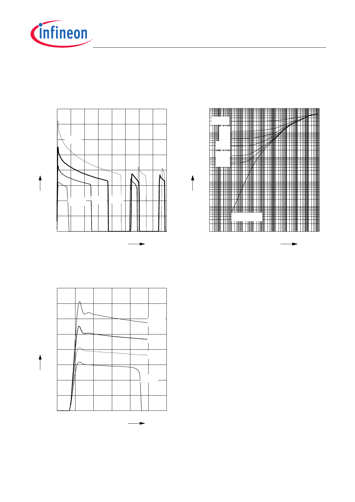
9 Typ. overload current
I
D(lim)
= f(
t), V
bb
=12 V, no heatsink
Parameter:
T
jstart
0
0.5
1
1.5
2
2.5
3
ms
4
t
0
5
10
15
20
25
30
A
40
I
D(lim)
-40°C
25°C
85°C
150°C
10 Typ. transient thermal impedance
Z
thJA
=f(
t
p
) @ 6 cm
2
cooling area
Parameter:
D=t
p
/
T
10
-7
10
-6
10
-5
10
-4
10
-3
10
-2
10
-1
10
0
10
1
10
3
s
t
p
-3
10
-2
10
-1
10
0
10
1
10
2
10
K/W
Z
thJA
Single pulse
0.01
0.02
0.05
0.1
0.2
D=0.5
11 Determination of
I
D(lim)
I
D(lim)
= f(
t); t
m
= 200µs
Parameter:
T
Jstart
0
0.1
0.2
0.3
0.4
ms
0.6
t
0
5
10
15
20
25
30
A
40
I
D(lim)
-40°C
25°C
85°C
150°C
Datasheet
8
Rev. 1.3, 2008-04-14
Smart Low Side Power Switch
HITFET BSP 78
Datasheet
9
Rev. 1.3, 2008-04-14
Smart Low Side Power Switch
HITFET BSP 78
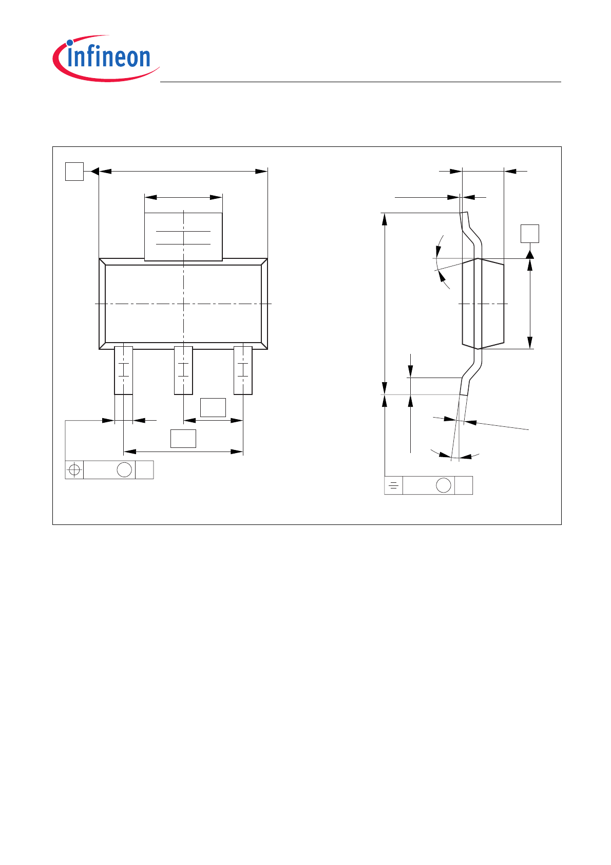
Package Outlines
1
Package Outlines
GPS05560
1
2
3
3
4
±0.1
±0.04
0.5 MIN.
0.28
0.1 MAX.
15˚ MAX.
6.5
±0.2
A
4.6
2.3
0.7
±0.1
0.25
M
A
1.6
±0.1
7
±0.3
B
0.25
M
±0.2
3.5
B
0...10˚
Figure 1
PG-SOT223-4 (Plastic Green Small Outline Transistor Package)
Green Product (RoHS compliant)
To meet the world-wide customer requirements for environmentally friendly products and to be compliant with
government regulations the device is available as a green product. Green products are RoHS-Compliant (i.e Pb-
free finish on leads and suitable for Pb-free soldering according to IPC/JEDEC J-STD-020).
Please specify the package needed (e.g. green package) when placing an order
You can find all of our packages, sorts of packing and others in our
Infineon Internet Page “Products”:
http://www.infineon.com/products
.
Dimensions in mm

Datasheet
10
Rev. 1.3, 2008-04-14
Smart Low Side Power Switch
HITFET BSP 78
Revision History
2
Revision History
Version
Date
Changes
Rev. 1.3
2008-04-14
Package information updated to SOT223-4
Rev. 1.2
2007-02-15
released automotive green version
Package parameter (humidity and climatic) removed in Maximum ratings
AEC icon added
RoHS icon added
Green product (RoHS-compliant) added to the feature list
Package information updated to green
Green explanation added
Rev. 1.1
2004-03-05
released production version