
Data Sheet Rev. 1.4
1
2008-07-10
Smart Lowside Power Switch
HITFET
BSP 75N
Data Sheet Rev. 1.4
Features
• Logic Level Input
• Input protection (ESD)
• Thermal shutdown with auto restart
• Overload protection
• Short circuit protection
• Overvoltage protection
• Current limitation
• Green Product (RoHS compliant)
• AEC Stress Test Qualification
Application
• All kinds of resistive, inductive and capacitive loads in switching applications
•
µC compatible power switch for 12 V and 24 V DC applications and for 42 Volt
Powernet
• Replaces electromechanical relays and discrete circuits
General Description
N channel vertical power FET in Smart Power Technology. Fully protected by embedded
protection functions.
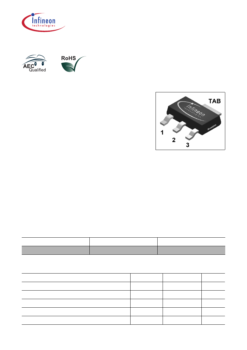
Type
Ordering Code
Package
HITFET
BSP 75N
on request
PG-SOT223-4
Product Summary
Parameter
Symbol
Value
Unit
Continuous drain source voltage
V
DS
60
V
On-state resistance
R
DS(ON)
550
m
Ω
Current limitation
I
D(lim)
1
A
Nominal load current
I
D(Nom)
0.7
A
Clamping energy
E
AS
550
mJ
HITFET
Logic
OUTPUT
Stage
Over voltage
Protection
IN
DRAIN
V
bb
dV/dt
limitation
SOURCE
ESD
Short circuit
Protection
Current
Limitation
Over
temperature
Protection
M
HITFET
BSP 75N
Data Sheet Rev. 1.4
2
2008-07-10
Figure 1
Block Diagram
1
2
3
TAB
IN
DRAIN
SOURCE
S
O
URCE
Figure 2
Pin Configuration
Pin Definitions and Functions
Pin No.
Symbol
Function
1
IN
Input; activates output and supplies internal logic
2
DRAIN
Output to the load
3 + TAB
SOURCE
Ground; pin3 and TAB are internally connected

Data Sheet Rev. 1.4
3
2008-07-10
HITFET
BSP 75N
Circuit Description
The BSP 75N is a monolithic power switch in Smart Power Technology (SPT) with a
logic level input, an open drain DMOS output stage and integrated protection functions.
It is designed for all kind of resistive and inductive loads (relays, solenoid) in automotive
and industrial applications.
Protection Functions
• Over voltage protection: An internal clamp limits the output voltage at
V
DS(AZ)
(min.
60V) when inductive loads are switched off.
• Current limitation: By means of an internal current measurement the drain current is
limited at
I
D(lim)
(1.4 - 1.5 A typ.). If the current limitation is active the device operates
in the linear region, so power dissipation may exceed the capability of the heatsink.
This operation leads to an increasing junction temperature until the over temperature
threshold is reached.
• Over temperature and short circuit protection: This protection is based on sensing
the chip temperature. The location of the sensor ensures a fast and accurate junction
temperature detection. Over temperature shutdown occurs at minimum 150
°C. A
hysteresis of typ. 10 K enables an automatic restart by cooling.
The device is ESD protected according Human Body Model (4 kV) and load dump
protected (see Maximum Ratings).

Absolute Maximum Ratings
T
j
= 25
°C, unless otherwise specified
Parameter
Symbol
Values
Unit Remarks
Continuous drain source voltage
1)
See also
Figure 7
and
Figure 10
.
1)
V
DS
60
V
–
Drain source voltage for
short circuit protection
V
DS
36
V
–
Continuous input voltage
V
IN
-0.2 … +10 V
–
Peak input voltage
V
IN
-0.2 … +20 V
–
Continuous Input Current
-0.2V
≤
V
IN
≤ 10V
V
IN
<-0.2V or
V
IN
>10V
I
IN
no limit
|
I
IN
|≤ 2mA
mA
–
Operating temperature range
Storage temperature range
T
j
T
stg
-40 … +150
-55 … +150
°C
°C
–
Power dissipation (DC)
P
tot
1.8
W
–
Unclamped single pulse inductive energy
E
AS
550
mJ
I
D(ISO)
= 0.7 A;
V
bb
=32V
Load dump protection
2)
V
LoadDump
is setup without DUT connected to the generator per ISO 7637-1 and DIN 40 839. See also
page 7
.
2)
IN = low or high (8 V);
R
L
= 50
Ω
IN = high (8 V);
R
L
= 22
Ω
V
LoadDump
80
47
V
V
LoadDump
=
V
P
+
V
S
;
V
P
= 13.5 V
R
3)
R
I
= internal resistance of the load dump test pulse generator LD200.
I
3)
= 2
Ω;
t
d
= 400 ms;
Electrostatic discharge voltage (Human
Body Model)
according to MIL STD 883D, method
3015.7 and EOS/ESD assn. standard
S5.1 - 1993
V
ESD
4000
V
–
Thermal Resistance
Junction soldering point
R
thJS
≤ 10
K/W –
Junction - ambient
4)
Device on epoxy pcb 40 mm
× 40 mm × 1.5 mm with 6 cm
2
copper area for pin 4 connection.
4)
R
thJA
≤ 70
K/W –
HITFET
BSP 75N
Data Sheet Rev. 1.4
4
2008-07-10

Data Sheet Rev. 1.4
5
2008-07-10
HITFET
BSP 75N
Electrical Characteristics
T
j
= 25
°C, unless otherwise specified
Parameter
Sym-
bol
Limit Values
Unit Test Conditions
min. typ.
max.
Static Characteristics
Drain source clamp voltage
V
DS(AZ)
60
–
75
V
I
D
= 10 mA,
T
j
= -40 … +150
°C
Off state drain current
I
DSS
–
–
5
µA
V
IN
= 0 V,
V
DS
= 32 V,
T
j
= -40 … +150
°C
Input threshold voltage
V
IN(th)
1
1.8
2.5
V
I
D
= 10 mA
Input current:
normal operation,
I
D
<
I
D(lim)
:
current limitation mode,
I
D
=
I
D(lim)
:
After thermal shutdown,
I
D
= 0 A:
I
IN(1)
I
IN(2)
I
IN(3)
–
–
1000
100
250
1500
200
400
2000
µA
V
IN
= 5 V
On-state resistance
T
j
= 25
°C
T
j
= 150
°C
R
DS(on)
–
–
490
850
675
1350
m
Ω
I
D
= 0.7 A,
V
IN
= 5 V
On-state resistance
T
j
= 25
°C
T
j
= 150
°C
R
DS(on)
–
–
430
750
550
1000
m
Ω
I
D
= 0.7 A,
V
IN
= 10 V
Nominal load current
I
D(Nom)
0.7
–
–
A
V
BB
= 12 V,
V
DS
= 0.5 V,
T
S
= 85
°C,
T
j
< 150
°C
Current limit
I
D(lim)
1
1.5
1.9
A
V
IN
= 10 V,
V
DS
= 12 V
Dynamic Characteristics
1)
Turn-on time
V
IN
to 90%
I
D
:
t
on
–
10
20
µs
R
L
= 22
Ω,
V
IN
= 0 to 10 V,
V
BB
= 12 V
Turn-off time
V
IN
to 10%
I
D
:
t
off
–
10
20
µs
R
L
= 22
Ω,
V
IN
= 10 to 0 V,
V
BB
= 12 V

HITFET
BSP 75N
Data Sheet Rev. 1.4
6
2008-07-10
Slew rate on
70 to 50%
V
BB
: -d
V
DS
/
d
t
on
–
5
10
V/
µs
R
L
= 22
Ω,
V
IN
= 0 to 10 V,
V
BB
= 12 V
Slew rate off
50 to 70%
V
BB
: d
V
DS
/
d
t
off
–
10
15
V/
µs
R
L
= 22
Ω,
V
IN
= 10 to 0 V,
V
BB
= 12 V
Protection Functions
2)
Thermal overload trip
temperature
T
jt
150
165
180
°C
–
Thermal hysteresis
∆
T
jt
–
10
–
Κ
–
Unclamped single pulse inductive
energy
T
j
= 25
°C
T
j
= 150
°C
E
AS
550
200
–
–
–
–
mJ
I
D(ISO)
= 0.7 A,
V
BB
= 32 V
Inverse Diode
Continuous source drain voltage
V
SD
–
1
–
V
V
IN
= 0 V,
-
I
D
= 2
× 0.7 A
1)
See also
Figure 9
.
2)
Integrated protection functions are designed to prevent IC destruction under fault conditions described in the
datasheet. Fault conditions are considered as “outside” normal operating range. Protection functions are not
designed for continuous, repetitive operation.
Electrical Characteristics (cont’d)
T
j
= 25
°C, unless otherwise specified
Parameter
Sym-
bol
Limit Values
Unit Test Conditions
min. typ.
max.

Data Sheet Rev. 1.4
7
2008-07-10
HITFET
BSP 75N
EMC-Characteristics
The following EMC-Characteristics outline the behavior of typical devices. They are not
part of any production test.
Table 1
Test Conditions
Parameter
Symbol
Value
Unit
Remark
Temperature
T
A
23
±5
°C
–
Supply Voltage
V
S
13.5
V
–
Load
R
L
27
Ω
ohmic
Operation mode
PWM
DC
–
–
–
–
f
INx
=100Hz, D=0.5
ON / OFF
DUT specific
V
IN
(’HIGH’)=5V
Fast electrical transients
acc. to ISO 7637
1)
The test pulses are applied at V
S
Test
1)
Pulse
1
-200V
C
C
500ms ; 10
Ω
2
+200V
C
C
500ms ; 10
Ω
3a
-200V
C
C
100ms ; 50
Ω
3b
+200V
C
C
100ms ; 50
Ω
4
-7V
C
C
0.01
Ω
5
175V
E(65V)
E(75V)
400ms ; 2
Ω
Definition of functional status
Class
Content
C
All functions of the device are performed as designed after exposure to
disturbance.
E
One or more function of a device does not perform as designed after
exposure and can not be returned to proper operation without repairing
or replacing the device. The value after the character shows the limit.
Max.
Test
Level
Test Result
Pulse Cycle Time
and Generator
Impedance
OUT
x
stressed
ON
OFF
BSP75N
SOURCE
DRAIN
IN
V
BB
R
L
PULSE
HITFET
BSP 75N
Data Sheet Rev. 1.4
8
2008-07-10
Figure 3
Test circuit for ISO pulse
Conducted Emissions
Acc. IEC 61967-4 (1
Ω/150Ω method)
Typ. V
bb
Emissions at PWM-mode with
150
Ω-matching network
-20
-10
0
10
20
30
40
50
60
70
80
90
100
0,1
1
10
100
1000
f / MHz
dB
µV
Noise level
BSP75N
150ohm Class6
150ohm Class1
150
Ω / 8-H
150
Ω / 13-N
150
Ω-Network
BSP75N
SOURCE
DRAIN
IN
V
BB
R
L
Figure 4
Test circuit for conducted
emission
1)
Conducted Susceptibility
Acc. 47A/658/CD IEC 62132-4 (Direct
Power Injection)
Direct Power Injection: Forward Power
CW
Failure Criteria: Amplitude or frequency
variation max. 10% at OUT
Typ. V
bb
Susceptibility at DC-ON/OFF
and at PWM
0
5
10
15
20
25
30
35
40
1
10
100
1000
f / MHz
dB
m
Limit
OUT, ON
OUT, OFF
OUT, PWM
HF
BSP75N
SOURCE
DRAIN
IN
V
BB
R
L
B A N
Test circuit for conducted susceptibility
2)
1)
For defined de coupling and high reproducibility a
defined choke (5
µH at 1MHz) is inserted in the
Vbb-Line.
2)
Broadband Artificial Network (short: BAN) consists
of the same choke (5
µH at 1MHz) and the same
150 Ohm-matching network as for emission
measurement for defined de coupling and high
reproducibility.
HITFET
BSP 75N
Data Sheet Rev. 1.4
9
2008-07-10
Block diagram
I
IN
V
IN
V
bb
I
D
HITFET
SOURCE
DRAIN
IN
V
DS
Figure 5
Terms
IN
SOURCE
Figure 6
Input Circuit (ESD
protection)
ESD zener diodes are not designed for DC
current.
Source
Drain
V
DS
I
D
V
AZ
Power
DMOS
LOAD
Figure 7
Inductive and Over
voltage Output Clamp
BSP75N
SOURCE
D
IN
V
BB
uC V
cc
GND
Px.1
Figure 8
Application Circuit
HITFET
BSP 75N
Data Sheet Rev. 1.4
10
2008-07-10
Timing diagrams
t
V
DS
t
I
D
t
on
t
off
0.9*I
D
0.1*I
D
V
IN
t
Figure 9
Switching a Resistive
Load
t
V
DS
t
I
D
V
BB
V
DS(AZ)
V
IN
t
Figure 10
Switching an Inducitve
Load
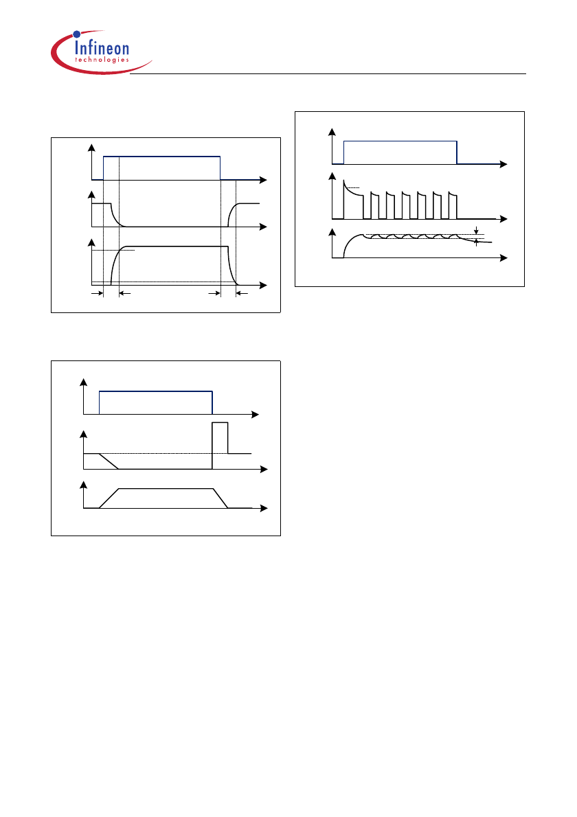
t
ϑ
j
I
D
t
thermal hysteresis
V
IN
t
I
D(lim)
Figure 11
Short circuit