

R F & P r o t e c t i o n D e v i c e s
P r e l i m i n a r y D a t a s h e e t
Rev. 1.3, 2013-03-29
B G S F 1 1 0 G N 2 6
SP10T Antenna Switch Module with integrated GPIO controller, 2 GSM-TX and 8
TRX Ports for multi-mode GSM/EDGE, WCDMA or LTE applications

Edition 2013-03-29
Published by
Infineon Technologies AG
81726 Munich, Germany
©
2013
Infineon Technologies AG
All Rights Reserved.
Legal Disclaimer
The information given in this document shall in no event be regarded as a guarantee of conditions or
characteristics. With respect to any examples or hints given herein, any typical values stated herein and/or any
information regarding the application of the device, Infineon Technologies hereby disclaims any and all warranties
and liabilities of any kind, including without limitation, warranties of non-infringement of intellectual property rights
of any third party.
Information
For further information on technology, delivery terms and conditions and prices, please contact the nearest
Infineon Technologies Office (
www.infineon.com
).
Warnings
Due to technical requirements, components may contain dangerous substances. For information on the types in
question, please contact the nearest Infineon Technologies Office.
Infineon Technologies components may be used in life-support devices or systems only with the express written
approval of Infineon Technologies, if a failure of such components can reasonably be expected to cause the failure
of that life-support device or system or to affect the safety or effectiveness of that device or system. Life support
devices or systems are intended to be implanted in the human body or to support and/or maintain and sustain
and/or protect human life. If they fail, it is reasonable to assume that the health of the user or other persons may
be endangered.

BGSF110GN26
SP10T Antenna Switch Module
Confidential
Preliminary Datasheet
3
Rev. 1.3, 2013-03-29
Trademarks of Infineon Technologies AG
AURIX™, C166™, CanPAK™, CIPOS™, CIPURSE™, EconoPACK™, CoolMOS™, CoolSET™,
CORECONTROL™, CROSSAVE™, DAVE™, DI-POL™, EasyPIM™, EconoBRIDGE™, EconoDUAL™,
EconoPIM™, EconoPACK™, EiceDRIVER™, eupec™, FCOS™, HITFET™, HybridPACK™, I²RF™,
ISOFACE™, IsoPACK™, MIPAQ™, ModSTACK™, my-d™, NovalithIC™, OptiMOS™, ORIGA™,
POWERCODE™; PRIMARION™, PrimePACK™, PrimeSTACK™, PRO-SIL™, PROFET™, RASIC™,
ReverSave™, SatRIC™, SIEGET™, SINDRION™, SIPMOS™, SmartLEWIS™, SOLID FLASH™, TEMPFET™,
thinQ!™, TRENCHSTOP™, TriCore™.
Other Trademarks
Advance Design System™ (ADS) of Agilent Technologies, AMBA™, ARM™, MULTI-ICE™, KEIL™,
PRIMECELL™, REALVIEW™, THUMB™, µVision™ of ARM Limited, UK. AUTOSAR™ is licensed by AUTOSAR
development partnership. Bluetooth™ of Bluetooth SIG Inc. CAT-iq™ of DECT Forum. COLOSSUS™,
FirstGPS™ of Trimble Navigation Ltd. EMV™ of EMVCo, LLC (Visa Holdings Inc.). EPCOS™ of Epcos AG.
FLEXGO™ of Microsoft Corporation. FlexRay™ is licensed by FlexRay Consortium. HYPERTERMINAL™ of
Hilgraeve Incorporated. IEC™ of Commission Electrotechnique Internationale. IrDA™ of Infrared Data
Association Corporation. ISO™ of INTERNATIONAL ORGANIZATION FOR STANDARDIZATION. MATLAB™ of
MathWorks, Inc. MAXIM™ of Maxim Integrated Products, Inc. MICROTEC™, NUCLEUS™ of Mentor Graphics
Corporation. MIPI™ of MIPI Alliance, Inc. MIPS™ of MIPS Technologies, Inc., USA. muRata™ of MURATA
MANUFACTURING CO., MICROWAVE OFFICE™ (MWO) of Applied Wave Research Inc., OmniVision™ of
OmniVision Technologies, Inc. Openwave™ Openwave Systems Inc. RED HAT™ Red Hat, Inc. RFMD™ RF
Micro Devices, Inc. SIRIUS™ of Sirius Satellite Radio Inc. SOLARIS™ of Sun Microsystems, Inc. SPANSION™
of Spansion LLC Ltd. Symbian™ of Symbian Software Limited. TAIYO YUDEN™ of Taiyo Yuden Co.
TEAKLITE™ of CEVA, Inc. TEKTRONIX™ of Tektronix Inc. TOKO™ of TOKO KABUSHIKI KAISHA TA. UNIX™
of X/Open Company Limited. VERILOG™, PALLADIUM™ of Cadence Design Systems, Inc. VLYNQ™ of Texas
Instruments Incorporated. VXWORKS™, WIND RIVER™ of WIND RIVER SYSTEMS, INC. ZETEX™ of Diodes
Zetex Limited.
Last Trademarks Update 2011-11-11
BGSF110GN26 SP10T Antenna Switch Module with integrated GPIO controller, 2 GSM-TX and 8 TRX Ports
for multi-mode GSM/EDGE, WCDMA or LTE applications
Confidential
Revision History: 2013-03-29, Rev. 1.3
Previous Revision:1.1
Page
Subjects (major changes since last revision)
12
Electrical charakteristics updated
15
Package outline drawing added
Product Name
Package
Marking
BGSF110GN26
PG-TSNP-26-2
F10G
SP10T Antenna Switch Module
BGSF110GN26
Preliminary Datasheet
4
Rev. 1.3, 2013-03-29
Confidential
1
Features
Main Features
•
Suitable for multi-mode GSM / EDGE / C2K / WCDMA / LTE
applications
•
0.1 to 3.8 GHz coverage
•
Ultra-low insertion loss and harmonics generation
•
Integrated GSM transmit filters
•
2 high-linearity GSM TX paths
•
8 high-linearity, interchangeable WCDMA TRX ports
•
2 TRX ports also function as high-linearity GSM RX ports
•
High port-to-port isolation
•
Integrated GPIO decoder supporting logic levels from 1.35 V to 3.1 V
•
No decoupling DC capacitors required, if no DC applied on RF lines
•
Small form factor 3.4 mm x 2.6 mm x 0.73 mm
•
1kV HBM ESD protection
Description
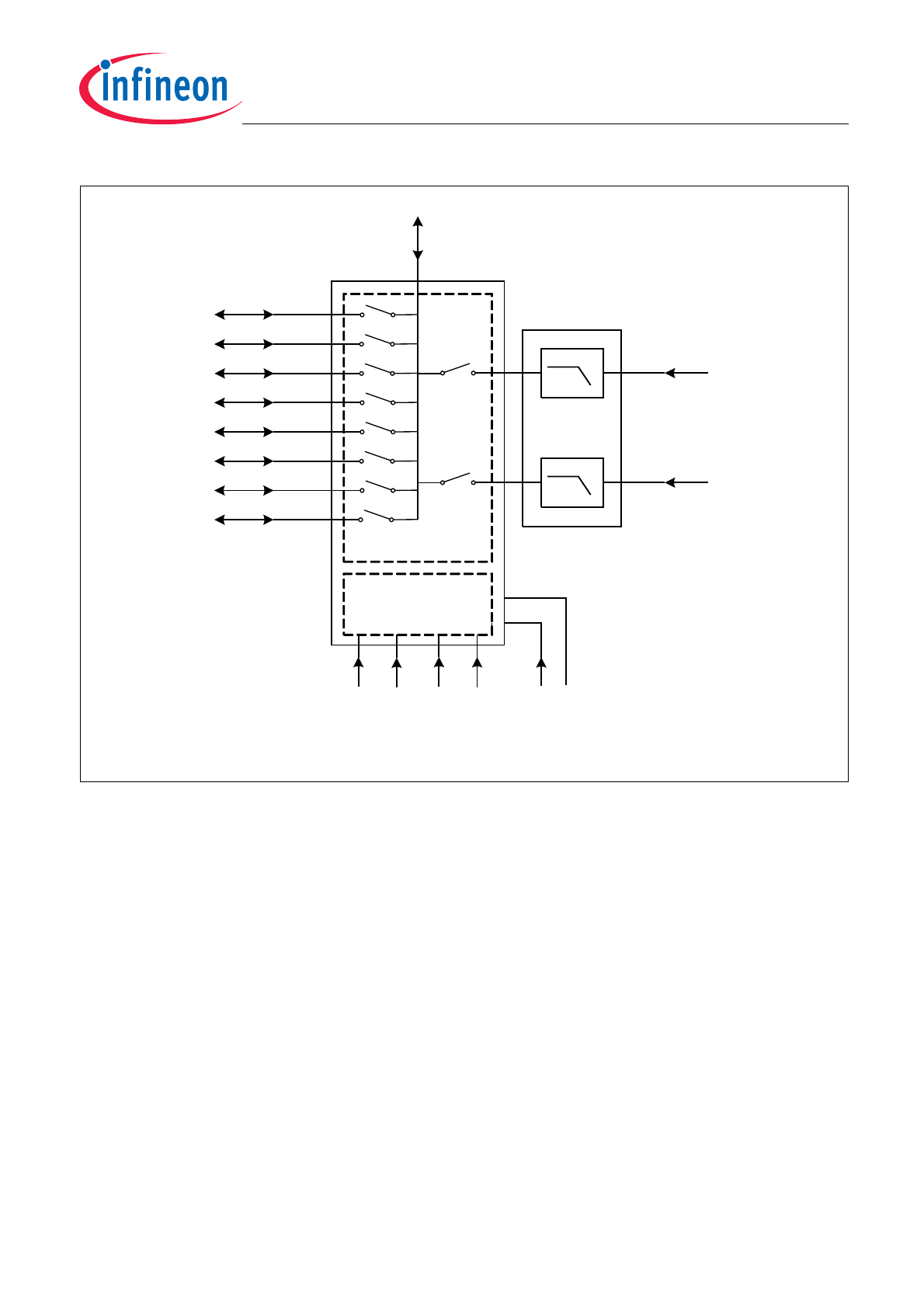
The BGSF110GN26 is a Single Pole Ten Throw (SP10T) Antenna Switch Module (ASM) optimized for wireless
applications up to 3.8 GHz. It is a perfect solution for multi-mode handsets based on quadband GSM, WCDMA
and LTE. The switch module configuration is shown in
Figure 1
.
The module comes in a miniature TSNP package and comprises of a high power CMOS SP10T switch with
integrated GPIO controller and harmonic filters for GSM high and low band transmit paths. The on-chip controller
integrates CMOS logic and level shifters, driven by control inputs from 1.35 to 3.1 V.
No external DC blocking capacitors are required in typical applications as long as no DC is applied to any RF port.
BGSF110GN26
SP10T Antenna Switch Module
Features
Confidential
Preliminary Datasheet
5
Rev. 1.3, 2013-03-29
Figure 1
Functional diagram
BGSF110G_Functional _Diagram.vsd
TX_HB
TX_LB
GPIO
Controller
Harmonic
Filters
V1
V2
VD
D
GN
D
V3
ANT
TRX1
TRX2
TRX3
TRX4
TRX5
TRX8
SP10T
TRX6
TRX7
V4
BGSF110GN26
SP10T Antenna Switch Module
Maximum Ratings
Confidential
Preliminary Datasheet
6
Rev. 1.3, 2013-03-29
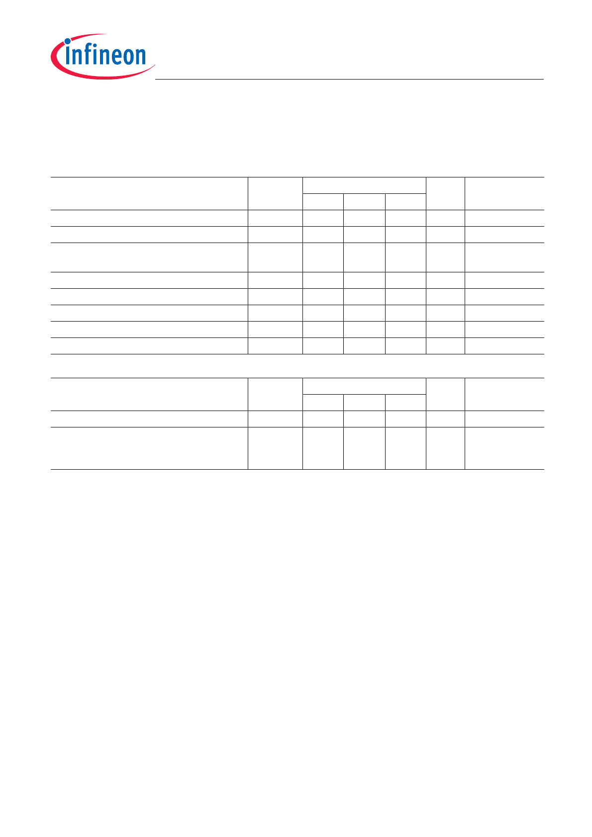
2
Maximum Ratings
Attention: Stresses above the max. values listed here may cause permanent damage to the device.
Exposure to absolute maximum rating conditions for extended periods may affect device
reliability. Maximum ratings are absolute ratings; exceeding only one of these values may
cause irreversible damage to the integrated circuit.
Table 1
Maximum Ratings
Parameter
Symbol
Values
Unit
Note /
Test Condition
Min.
Typ.
Max.
Supply voltage
V
dd
-0.5
–
3.6
V
–
GPIO control voltage levels
V
CtrlX
-0.7
–
V
dd
+0.7 V
–
Maximum DC-voltage on RF-ports and RF-
grounds
V
RFDC
0
–
0
V
–
Storage Temperature Range
T
stg
-65
–
150
°C
–
Junction temperature
T
j
–
–
125
°C
–
Thermal resistance junction - soldering point
R
thJS
–
32
–
K/W
–
RF input power at all GSM TX ports
P
RF_TX
–
–
36
dBm
CW
RF input power at all TRX ports
P
RF_TRX
–
–
30
dBm
CW
Table 2
ESD Ratings
Parameter
Symbol
Values
Unit
Note /
Test Condition
Min.
Typ.
Max.
ESD capability Human Body Model
V
ESD_HBM
–
1000
–
V
–
ESD capability ANT port (according IEC
6100-4-2 contact)
V
ESD_ANT
–
tbd
–
V
Using external
shunt inductor
on ANT port
BGSF110GN26
SP10T Antenna Switch Module
Operation Ranges
Confidential
Preliminary Datasheet
7
Rev. 1.3, 2013-03-29
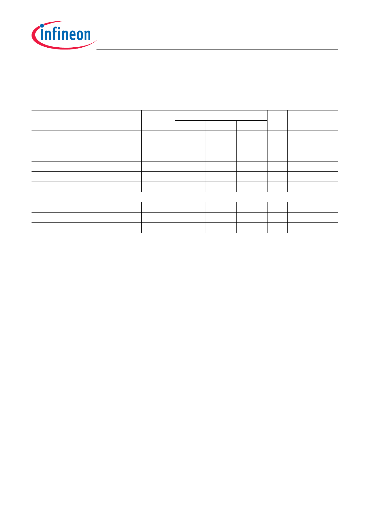
3
Operation Ranges
Table 3
Operation Ranges
Parameter
Symbol
Values
Unit
Note /
Test Condition
Min.
Typ.
Max.
Supply Voltage
V
dd
2.4
3.0
3.3
V
–
Supply current
I
dd
–
100
200
μA
–
Ambient temperature range
T
A
-30
–
+85
°C
–
Extended temperature range
T
E
-40
–
+95
°C
Functional only
Control voltage High
V
CtrlH
1.35
1.8
V
dd
V
–
Control voltage Low
V
CtrlL
0
–
0.45
V
–
Input Power
TRX ports
P
in_TRX
–
–
27
dBm
–
GSM TX LB port
P
in_GSM_LB
–
–
36
dBm
50% duty cycle
GSM TX HB port
P
in_GSM_HB
–
–
34
dBm
50% duty cycle
BGSF110GN26
SP10T Antenna Switch Module
Electrical Characteristics
Confidential
Preliminary Datasheet
8
Rev. 1.3, 2013-03-29
4
Electrical Characteristics
Terminating port impedance:
Z
0
= 50
Ω
Temperature:
T
= -25 °C – +85 °C
Supply voltage:
V
dd
= 2.4 V.. 3.3 V
Unless otherwise specified
Table 4
RF Characteristics
Parameter
Symbol
Values
Unit
Note / Test Condition
Min.
Typ.
Max.
Insertion Loss
TRX1-8
IL
–
0.50
0.70
dB
698 to 960 MHz
–
0.58
0.78
dB
1428 to 1990 MHz
–
0.62
0.82
dB
1990 to 2170 MHz
–
0.75
1.00
dB
2170 to 2690 MHz
–
1.12
1.42
dB
2690 to 3500 MHz
–
1.35
1.63
dB
3600 to 3800 MHz
TXLB
IL
–
0.90
1.20
dB
824 to 915 MHz
TXHB
IL
–
1.00
1.30
dB
1710 to 1910 MHz
Return Loss
RL
25
30
–
dB
698 to 960 MHz
23
27
–
dB
1710 to 1990 MHz
21
25
–
dB
1990 to 2170 MHz
18
23
–
dB
2170 to 2690 MHz
13
16
–
dB
2690 to 3500 MHz
Isolation (f = 698-2690 MHz unless noted otherwise)
ISO
32
40
–
dB
TRX1,2,3,7,8 to TRX4,5,6 (f = 698 - 2400 MHz)
28
32
–
dB
TRX1,2,3,7,8 to TRX4,5,6 (f = 2400- 2690
MHz)
37
46
–
dB
TX1 to all TRXports (f = 824-915 MHz)
37
40
–
dB
TX2 to all TRXports (f = 1710-1910 MHz)
27
37
–
dB
TRX4 to TRX6
19
25
–
dB
TRX1 to TRX2, TRX2 to TRX3, TRX4 to TRX5,
TRX5 to TRX6
34
35
–
dB
ANT to TRX7 (RX1) (active path: ANT - TRX8)
(f = 1805-1910 MHz)
37
40
–
dB
ANT to TRX8 (RX2) (active path: ANT - TRX7)
(f = 1805-1910 MHz)
Switching Time
On/Off
t
on/off
–
1
–
μs
90% OFF to 90% ON; 90% ON to 90% OFF
BGSF110GN26
SP10T Antenna Switch Module
Electrical Characteristics
Confidential
Preliminary Datasheet
9
Rev. 1.3, 2013-03-29
Note: All electrical characteristics are measured with all RF ports terminated in 50
Ω
and recommended circuit.
Boost Converter
Settling Time
t
BC
–
–
25
μs
After power down mode
Intermodulation Distortion (UMTS Band 1, Band 5)
IMD2, low
IMD2 low
–
-102
-97
dBm
Tx = 20 dBm, Interferer = -15 dBm
IMD2, high
IMD2 high
–
-105
-97
dBm
Tx = 20 dBm, Interferer = -15 dBm
IMD3
IMD3
–
-115
-97
dBm
Tx = 20 dBm, Interferer = -15 dBm
Harmonic Generation up to 12.75 GHz
TXLB, H2
P
Harm
77
88
–
dBc
35 dBm, 50
Ω, 50% duty cycle
TXLB, H3
86
100
–
dBc
35 dBm, 50
Ω, 50% duty cycle
TXHB, H2
82
98
–
dBc
32 dBm, 50
Ω, 50% duty cycle
TXHB, H3
77
82
–
dBc
32 dBm, 50
Ω, 50% duty cycle
TRX1-8, H2
81
88
–
dBc
25 dBm, 50
Ω
TRX1-8, H3
85
97
–
dBc
25 dBm, 50
Ω
Harmonic Attenuation
TXLB
P
att
27
38
–
dB
1648 to 1830 MHz
27
33
–
dB
2472 to 2745 MHz
20
27
–
dB
2746 to 12750 MHz
TXHB
27
38
–
dB
3420 to 3820 MHz
25
30
–
dB
5130 to 5730 MHz
23
27
–
dB
5731 to 12750 MHz
Table 4
RF Characteristics (cont’d)
Parameter
Symbol
Values
Unit
Note / Test Condition
Min.
Typ.
Max.

BGSF110GN26
SP10T Antenna Switch Module
Pin Definition and Package Outline
Confidential
Preliminary Datasheet
10
Rev. 1.3, 2013-03-29
5
Pin Definition and Package Outline
Table 5
Pin Configuration
Pin No.
Name
Pin
Type
Buffer
Type
Function
0
GND
GND
Ground, Die Pad
1
GND
GND
RF Ground
2
TRX4
I/O
WCDMA TRX-Port
3
TRX5
I/O
WCDMA TRX-Port
4
TRX6
I/O
WCDMA TRX-Port
5
GND
GND
RF Ground
6
GND
GND
RF Ground
7
ANT
I/O
Antenna Port
8
GND
GND
RF Ground
9
GND
GND
RF Ground
10
TX2
I
GSM HB-Port
11
GND
GND
RF Ground
12
GND
GND
RF Ground
13
TX1
I
GSM LB-Port
14
GND
GND
RF Ground
15
TRX8
I/O
WCDMA TRX-Port (GSM RX-Port)
16
GND
GND
RF Ground
17
TRX7
I/O
WCDMA TRX-Port (GSM RX-Port)
18
TRX1
I/O
WCDMA TRX-Port
19
TRX2
I/O
WCDMA TRX-Port
20
TRX3
I/O
WCDMA TRX-Port
21
GND
GND
DC Ground
22
VDD
PWR
Supply Voltage
23
V4
I
GPIO Control Ping
24
V3
I
GPIO Control Pin
25
V2
I
GPIO Control Pin
26
V1
I
GPIO Control Pin
Table 6
Mechanical Data
Parameter
Symbol
Value
Unit
Package size
Size
3.4 x 2.6
mm
Package height
H
0.73
mm