

R F & P r o t e c t i o n D e v i c e s
D a t a S h e e t
Revision 3.1, 2013-01-31
B G A 7 5 1 N 7
SiGe Bipolar 3G/3.5G/4G Single-Band LNA

Edition 2013-01-31
Published by
Infineon Technologies AG
81726 Munich, Germany
©
2013
Infineon Technologies AG
All Rights Reserved.
Legal Disclaimer
The information given in this document shall in no event be regarded as a guarantee of conditions or
characteristics. With respect to any examples or hints given herein, any typical values stated herein and/or any
information regarding the application of the device, Infineon Technologies hereby disclaims any and all warranties
and liabilities of any kind, including without limitation, warranties of non-infringement of intellectual property rights
of any third party.
Information
For further information on technology, delivery terms and conditions and prices, please contact the nearest
Infineon Technologies Office (
www.infineon.com
).
Warnings
Due to technical requirements, components may contain dangerous substances. For information on the types in
question, please contact the nearest Infineon Technologies Office.
Infineon Technologies components may be used in life-support devices or systems only with the express written
approval of Infineon Technologies, if a failure of such components can reasonably be expected to cause the failure
of that life-support device or system or to affect the safety or effectiveness of that device or system. Life support
devices or systems are intended to be implanted in the human body or to support and/or maintain and sustain
and/or protect human life. If they fail, it is reasonable to assume that the health of the user or other persons may
be endangered.
BGA751N7
SiGe Bipolar 3G/3.5G/4G Single-Band LNA
Data Sheet
3
Revision 3.1, 2013-01-31
Trademarks of Infineon Technologies AG
AURIX™, C166™, CanPAK™, CIPOS™, CIPURSE™, EconoPACK™, CoolMOS™, CoolSET™,
CORECONTROL™, CROSSAVE™, DAVE™, DI-POL™, EasyPIM™, EconoBRIDGE™, EconoDUAL™,
EconoPIM™, EconoPACK™, EiceDRIVER™, eupec™, FCOS™, HITFET™, HybridPACK™, I²RF™,
ISOFACE™, IsoPACK™, MIPAQ™, ModSTACK™, my-d™, NovalithIC™, OptiMOS™, ORIGA™,
POWERCODE™; PRIMARION™, PrimePACK™, PrimeSTACK™, PRO-SIL™, PROFET™, RASIC™,
ReverSave™, SatRIC™, SIEGET™, SINDRION™, SIPMOS™, SmartLEWIS™, SOLID FLASH™, TEMPFET™,
thinQ!™, TRENCHSTOP™, TriCore™.
Other Trademarks
Advance Design System™ (ADS) of Agilent Technologies, AMBA™, ARM™, MULTI-ICE™, KEIL™,
PRIMECELL™, REALVIEW™, THUMB™, µVision™ of ARM Limited, UK. AUTOSAR™ is licensed by AUTOSAR
development partnership. Bluetooth™ of Bluetooth SIG Inc. CAT-iq™ of DECT Forum. COLOSSUS™,
FirstGPS™ of Trimble Navigation Ltd. EMV™ of EMVCo, LLC (Visa Holdings Inc.). EPCOS™ of Epcos AG.
FLEXGO™ of Microsoft Corporation. FlexRay™ is licensed by FlexRay Consortium. HYPERTERMINAL™ of
Hilgraeve Incorporated. IEC™ of Commission Electrotechnique Internationale. IrDA™ of Infrared Data
Association Corporation. ISO™ of INTERNATIONAL ORGANIZATION FOR STANDARDIZATION. MATLAB™ of
MathWorks, Inc. MAXIM™ of Maxim Integrated Products, Inc. MICROTEC™, NUCLEUS™ of Mentor Graphics
Corporation. MIPI™ of MIPI Alliance, Inc. MIPS™ of MIPS Technologies, Inc., USA. muRata™ of MURATA
MANUFACTURING CO., MICROWAVE OFFICE™ (MWO) of Applied Wave Research Inc., OmniVision™ of
OmniVision Technologies, Inc. Openwave™ Openwave Systems Inc. RED HAT™ Red Hat, Inc. RFMD™ RF
Micro Devices, Inc. SIRIUS™ of Sirius Satellite Radio Inc. SOLARIS™ of Sun Microsystems, Inc. SPANSION™
of Spansion LLC Ltd. Symbian™ of Symbian Software Limited. TAIYO YUDEN™ of Taiyo Yuden Co.
TEAKLITE™ of CEVA, Inc. TEKTRONIX™ of Tektronix Inc. TOKO™ of TOKO KABUSHIKI KAISHA TA. UNIX™
of X/Open Company Limited. VERILOG™, PALLADIUM™ of Cadence Design Systems, Inc. VLYNQ™ of Texas
Instruments Incorporated. VXWORKS™, WIND RIVER™ of WIND RIVER SYSTEMS, INC. ZETEX™ of Diodes
Zetex Limited.
Last Trademarks Update 2011-11-11
BGA751N7 SiGe Bipolar 3G/3.5G/4G Single-Band LNA
Revision History: 2013-01-31, Revision 3.1
Previous Revision: 2012-10-31, Revision 3.0
Page
Subjects (major changes since last revision)
37
Footprint recommendation drawing added
38
Marking pattern drawing updated

BGA751N7
SiGe Bipolar 3G/3.5G/4G Single-Band LNA
Table of Contents
Data Sheet
4
Revision 3.1, 2013-01-31
Table of Contents . . . . . . . . . . . . . . . . . . . . . . . . . . . . . . . . . . . . . . . . . . . . . . . . . . . . . . . . . . . . . . . . 4
List of Figures . . . . . . . . . . . . . . . . . . . . . . . . . . . . . . . . . . . . . . . . . . . . . . . . . . . . . . . . . . . . . . . . . . . 5
List of Tables . . . . . . . . . . . . . . . . . . . . . . . . . . . . . . . . . . . . . . . . . . . . . . . . . . . . . . . . . . . . . . . . . . . . 6
1
Features . . . . . . . . . . . . . . . . . . . . . . . . . . . . . . . . . . . . . . . . . . . . . . . . . . . . . . . . . . . . . . . . . . . . . . . . 7
2
Electrical Characteristics . . . . . . . . . . . . . . . . . . . . . . . . . . . . . . . . . . . . . . . . . . . . . . . . . . . . . . . . . . 9
2.1
Absolute Maximum Ratings . . . . . . . . . . . . . . . . . . . . . . . . . . . . . . . . . . . . . . . . . . . . . . . . . . . . . . . . . 9
2.2
Thermal Resistance . . . . . . . . . . . . . . . . . . . . . . . . . . . . . . . . . . . . . . . . . . . . . . . . . . . . . . . . . . . . . . . 9
2.3
ESD Integrity . . . . . . . . . . . . . . . . . . . . . . . . . . . . . . . . . . . . . . . . . . . . . . . . . . . . . . . . . . . . . . . . . . . . . 9
2.4
DC Characteristics . . . . . . . . . . . . . . . . . . . . . . . . . . . . . . . . . . . . . . . . . . . . . . . . . . . . . . . . . . . . . . . 10
2.5
Gain Mode Select Truth Table . . . . . . . . . . . . . . . . . . . . . . . . . . . . . . . . . . . . . . . . . . . . . . . . . . . . . . 10
2.6
Switching Times . . . . . . . . . . . . . . . . . . . . . . . . . . . . . . . . . . . . . . . . . . . . . . . . . . . . . . . . . . . . . . . . . 10
2.7
Supply Current Characteristics . . . . . . . . . . . . . . . . . . . . . . . . . . . . . . . . . . . . . . . . . . . . . . . . . . . . . . 11
2.8
Logic Signal Characteristics . . . . . . . . . . . . . . . . . . . . . . . . . . . . . . . . . . . . . . . . . . . . . . . . . . . . . . . . 12
2.9
Measured RF Characteristics 700 MHz Band . . . . . . . . . . . . . . . . . . . . . . . . . . . . . . . . . . . . . . . . . . 13
2.10
Measured RF Characteristics 750 MHz Band . . . . . . . . . . . . . . . . . . . . . . . . . . . . . . . . . . . . . . . . . . 14
2.11
Measured RF Characteristics 800 MHz Band . . . . . . . . . . . . . . . . . . . . . . . . . . . . . . . . . . . . . . . . . . 15
2.12
Measured RF Characteristics 880 MHz Band . . . . . . . . . . . . . . . . . . . . . . . . . . . . . . . . . . . . . . . . . . 16
2.13
Measured RF Characteristics 900 MHz band . . . . . . . . . . . . . . . . . . . . . . . . . . . . . . . . . . . . . . . . . . . 17
2.14
Measured RF Characteristics 1100 MHz band . . . . . . . . . . . . . . . . . . . . . . . . . . . . . . . . . . . . . . . . . . 18
2.15
Measured Performance Band 13 Application High Gain Mode vs. Frequency . . . . . . . . . . . . . . . . . . 19
2.16
Measured Performance Band 13 Application High Gain Mode vs. Temperature . . . . . . . . . . . . . . . . 20
2.17
Measured Performance Band 13 Application Low Gain Mode vs. Frequency . . . . . . . . . . . . . . . . . . 21
2.18
Measured Performance Band 13 Application Low Gain Mode vs. Temperature . . . . . . . . . . . . . . . . 22
2.19
Measured Performance Band 5 Application High Gain Mode vs. Frequency . . . . . . . . . . . . . . . . . . . 23
2.20
Measured Performance Band 5 Application High Gain Mode vs. Temperature . . . . . . . . . . . . . . . . . 25
2.21
Measured Performance Band 5 Application Low Gain Mode vs. Frequency . . . . . . . . . . . . . . . . . . . 26
2.22
Measured Performance Band 5 Application Low Gain Mode vs. Temperature . . . . . . . . . . . . . . . . . 28
3
Application Circuit and Block Diagram . . . . . . . . . . . . . . . . . . . . . . . . . . . . . . . . . . . . . . . . . . . . . 29
3.1
700 MHz Band Application Circuit Schematic . . . . . . . . . . . . . . . . . . . . . . . . . . . . . . . . . . . . . . . . . . 29
3.2
750 MHz Band Application Circuit Schematic . . . . . . . . . . . . . . . . . . . . . . . . . . . . . . . . . . . . . . . . . . 30
3.3
800 MHz Band Application Circuit Schematic . . . . . . . . . . . . . . . . . . . . . . . . . . . . . . . . . . . . . . . . . . 31
3.4
880 MHz Band Application Circuit Schematic . . . . . . . . . . . . . . . . . . . . . . . . . . . . . . . . . . . . . . . . . . 32
3.5
900 MHz Band Application Circuit Schematic . . . . . . . . . . . . . . . . . . . . . . . . . . . . . . . . . . . . . . . . . . 33
3.6
1100 MHz Band Application Circuit Schematic . . . . . . . . . . . . . . . . . . . . . . . . . . . . . . . . . . . . . . . . . 34
3.7
Pin Definition . . . . . . . . . . . . . . . . . . . . . . . . . . . . . . . . . . . . . . . . . . . . . . . . . . . . . . . . . . . . . . . . . . . . 34
3.8
Application Board . . . . . . . . . . . . . . . . . . . . . . . . . . . . . . . . . . . . . . . . . . . . . . . . . . . . . . . . . . . . . . . . 35
4
Physical Characteristics . . . . . . . . . . . . . . . . . . . . . . . . . . . . . . . . . . . . . . . . . . . . . . . . . . . . . . . . . 37
4.1
Package Footprint . . . . . . . . . . . . . . . . . . . . . . . . . . . . . . . . . . . . . . . . . . . . . . . . . . . . . . . . . . . . . . . . 37
4.2
Package Dimensions . . . . . . . . . . . . . . . . . . . . . . . . . . . . . . . . . . . . . . . . . . . . . . . . . . . . . . . . . . . . . 38
4.3
Product Marking Pattern . . . . . . . . . . . . . . . . . . . . . . . . . . . . . . . . . . . . . . . . . . . . . . . . . . . . . . . . . . . 38
Table of Contents

BGA751N7
SiGe Bipolar 3G/3.5G/4G Single-Band LNA
List of Figures
Data Sheet
5
Revision 3.1, 2013-01-31
Figure 1
Block Diagram of Single-Band LNA . . . . . . . . . . . . . . . . . . . . . . . . . . . . . . . . . . . . . . . . . . . . . . . . . 8
Figure 2
Application Circuit with Chip Outline (top view) . . . . . . . . . . . . . . . . . . . . . . . . . . . . . . . . . . . . . . . 29
Figure 3
Application Circuit with Chip Outline (top view) . . . . . . . . . . . . . . . . . . . . . . . . . . . . . . . . . . . . . . . 30
Figure 4
Application Circuit with Chip Outline (top view) . . . . . . . . . . . . . . . . . . . . . . . . . . . . . . . . . . . . . . . 31
Figure 5
Application Circuit with Chip Outline (top view) . . . . . . . . . . . . . . . . . . . . . . . . . . . . . . . . . . . . . . . 32
Figure 6
Application Circuit with Chip Outline (top view) . . . . . . . . . . . . . . . . . . . . . . . . . . . . . . . . . . . . . . . 33
Figure 7
Application Circuit with Chip Outline (top view) . . . . . . . . . . . . . . . . . . . . . . . . . . . . . . . . . . . . . . . 34
Figure 8
Application Board Layout on 3-layer FR4 . . . . . . . . . . . . . . . . . . . . . . . . . . . . . . . . . . . . . . . . . . . . 35
Figure 9
Cross-Section view of Application Board . . . . . . . . . . . . . . . . . . . . . . . . . . . . . . . . . . . . . . . . . . . . 35
Figure 10
Detail of Application Board Layout . . . . . . . . . . . . . . . . . . . . . . . . . . . . . . . . . . . . . . . . . . . . . . . . . 36
Figure 11
Footprint Recommendation 1 for the TSNP-7-1 Package . . . . . . . . . . . . . . . . . . . . . . . . . . . . . . . 37
Figure 12
Footprint Recommendation 2 for the TSNP-7-1 Package . . . . . . . . . . . . . . . . . . . . . . . . . . . . . . . 37
Figure 13
Package Outline (top, side and bottom view) . . . . . . . . . . . . . . . . . . . . . . . . . . . . . . . . . . . . . . . . . 38
Figure 14
Tape & Reel Dimensions . . . . . . . . . . . . . . . . . . . . . . . . . . . . . . . . . . . . . . . . . . . . . . . . . . . . . . . . 38
Figure 15
Marking Pattern (top view) . . . . . . . . . . . . . . . . . . . . . . . . . . . . . . . . . . . . . . . . . . . . . . . . . . . . . . . 38
List of Figures

BGA751N7
SiGe Bipolar 3G/3.5G/4G Single-Band LNA
List of Tables
Data Sheet
6
Revision 3.1, 2013-01-31
Table 1
Absolute Maximum Ratings . . . . . . . . . . . . . . . . . . . . . . . . . . . . . . . . . . . . . . . . . . . . . . . . . . . . . . . 9
Table 2
Thermal Resistance . . . . . . . . . . . . . . . . . . . . . . . . . . . . . . . . . . . . . . . . . . . . . . . . . . . . . . . . . . . . . 9
Table 3
ESD Integrity . . . . . . . . . . . . . . . . . . . . . . . . . . . . . . . . . . . . . . . . . . . . . . . . . . . . . . . . . . . . . . . . . . 9
Table 4
DC Characteristics,
T
A
= 25 °C . . . . . . . . . . . . . . . . . . . . . . . . . . . . . . . . . . . . . . . . . . . . . . . . . . . 10
Table 5
Truth Table . . . . . . . . . . . . . . . . . . . . . . . . . . . . . . . . . . . . . . . . . . . . . . . . . . . . . . . . . . . . . . . . . . 10
Table 6
Typical switching times;
T
A
= -30 ... 85 °C . . . . . . . . . . . . . . . . . . . . . . . . . . . . . . . . . . . . . . . . . . . 10
Table 7
Typical Characteristics 700 MHz Band,
T
A
= 25 °C,
V
CC
= 2.8 V,
R
REF
= 5.6 k
Ω . . . . . . . . . . . . . . 13
Table 8
Typical Characteristics 750 MHz Band,
T
A
= 25 °C,
V
CC
= 2.8 V,
R
REF
= 5.6 k
Ω . . . . . . . . . . . . . . 14
Table 9
Typical Characteristics 800 MHz Band,
T
A
= 25 °C,
V
CC
= 2.8 V,
R
REF
= 5.6 k
Ω . . . . . . . . . . . . . . 15
Table 10
Typical Characteristics 880 MHz Band,
T
A
= 25 °C,
V
CC
= 2.8 V,
R
REF
= n/c . . . . . . . . . . . . . . . . 16
Table 11
Typical Characteristics 900 MHz Band,
T
A
= 25 °C,
V
CC
= 2.8 V,
R
REF
= n/c . . . . . . . . . . . . . . . . . 17
Table 12
Typical Characteristics 1100 MHz Band,
T
A
= 25 °C,
V
CC
= 2.8 V,
R
REF
= 8.2 k
Ω . . . . . . . . . . . . . 18
Table 13
Parts List . . . . . . . . . . . . . . . . . . . . . . . . . . . . . . . . . . . . . . . . . . . . . . . . . . . . . . . . . . . . . . . . . . . . 29
Table 14
Parts List . . . . . . . . . . . . . . . . . . . . . . . . . . . . . . . . . . . . . . . . . . . . . . . . . . . . . . . . . . . . . . . . . . . . 30
Table 15
Parts List . . . . . . . . . . . . . . . . . . . . . . . . . . . . . . . . . . . . . . . . . . . . . . . . . . . . . . . . . . . . . . . . . . . . 31
Table 16
Parts List . . . . . . . . . . . . . . . . . . . . . . . . . . . . . . . . . . . . . . . . . . . . . . . . . . . . . . . . . . . . . . . . . . . . 32
Table 17
Parts List . . . . . . . . . . . . . . . . . . . . . . . . . . . . . . . . . . . . . . . . . . . . . . . . . . . . . . . . . . . . . . . . . . . . 33
Table 18
Parts List . . . . . . . . . . . . . . . . . . . . . . . . . . . . . . . . . . . . . . . . . . . . . . . . . . . . . . . . . . . . . . . . . . . . 34
Table 19
Pin Definition and Function . . . . . . . . . . . . . . . . . . . . . . . . . . . . . . . . . . . . . . . . . . . . . . . . . . . . . . 34
List of Tables
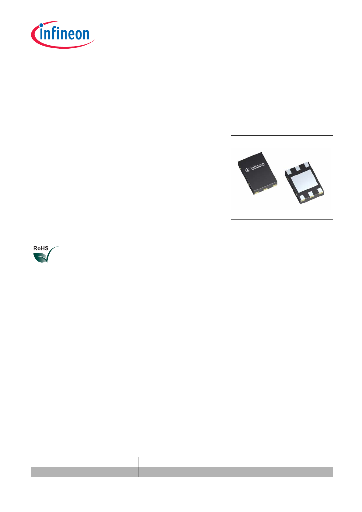
Product Name
Package
Chip
Marking
BGA751N7
TSNP-7-1
T1533
B5
SiGe Bipolar 3G/3.5G/4G Single-Band LNA
BGA751N7
Data Sheet
7
Revision 3.1, 2013-01-31
1
Features
Main features:
•
Gain: 16 / -8 dB in high / low gain mode (f.e. at 850MHz)
•
Noise figure: 1.05 dB in high gain mode (f.e. at 850MHz)
•
Supply current: 3.3 / 0.5 mA in high / low gain mode
•
Standby mode (< 2
μA typ.)
•
Output internally matched to 50
Ω
•
Inputs pre-matched to 50
Ω
•
2 kV HBM ESD protection
•
Low external component count
•
Small leadless TSNP-7-1 package (2.0 x 1.3 x 0.39 mm)
•
Pb-free (RoHS compliant) package
Description
The BGA751N7 is a low current single-band low noise amplifier MMIC for 3G, 3.5G and 4G. The LNA is based
upon Infineon’s proprietary and cost-effective SiGe:C technology and comes in a low profile TSNP-7-1 leadless
green package. Because the matching is off chip, the RFpath can be easily converted into a 700MHz to 1150MHz
path by optimizing the input and output matching network. This document specifies the electrical parameters,
pinout, application circuit and packaging of the chip.
BGA751N7
SiGe Bipolar 3G/3.5G/4G Single-Band LNA
Features
Data Sheet
8
Revision 3.1, 2013-01-31
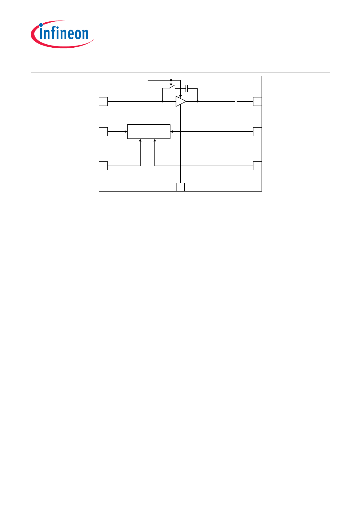
Figure 1
Block Diagram of Single-Band LNA
BGA751N7_Chip_BlD.vsd
3
2
1
4
5
6
Biasing & Logic
Circuitry
RFOUT
RREF
VCC
RFIN
VEN
7
GND
VGS
BGA751N7
SiGe Bipolar 3G/3.5G/4G Single-Band LNA
Electrical Characteristics
Data Sheet
9
Revision 3.1, 2013-01-31
2
Electrical Characteristics
2.1
Absolute Maximum Ratings
Attention: Stresses above the max. values listed here may cause permanent damage to the device.
Exposure to absolute maximum rating conditions for extended periods may affect device
reliability. Maximum ratings are absolute ratings; exceeding only one of these values may
cause irreversible damage to the integrated circuit.
2.2
Thermal Resistance
2.3
ESD Integrity
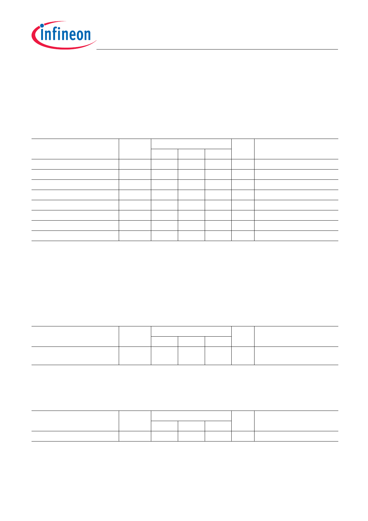
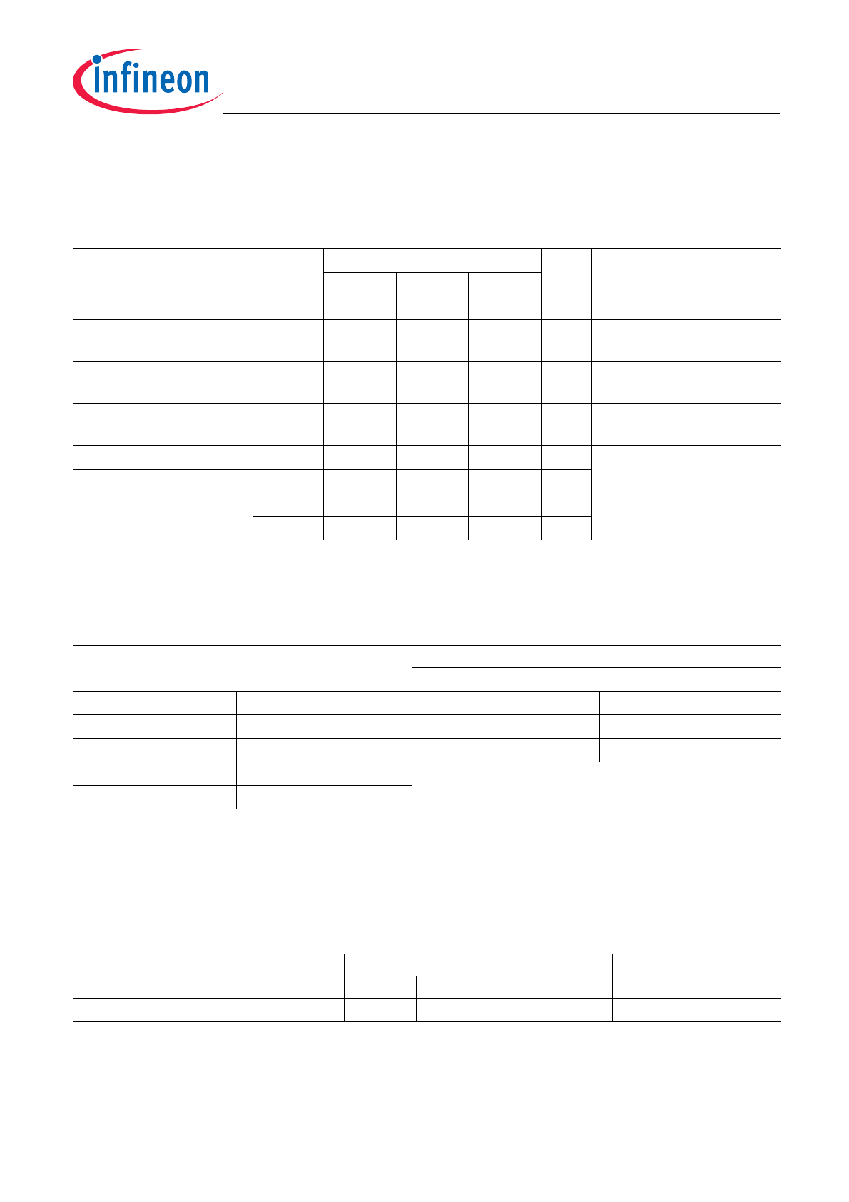
Table 1
Absolute Maximum Ratings
Parameter
Symbol
Values
Unit
Note / Test Condition
Min.
Typ.
Max.
Supply voltage
V
CC
-0.3
–
3.6
V
–
Supply current
I
CC
–
–
10
mA
–
Pin voltage
V
PIN
-0.3
–
V
CC
+0.3 V
All pins except RF input pins.
Pin voltage RF Input Pins
V
RFIN
-0.3
–
0.9
V
–
RF input power
P
RFIN
–
–
4
dBm
–
Junction temperature
T
j
–
–
150
°C
–
Ambient temperature range
T
A
-30
–
85
°C
–
Storage temperature range
T
stg
-65
–
150
°C
–
Table 2
Thermal Resistance
Parameter
Symbol
Values
Unit
Note / Test Condition
Min.
Typ.
Max.
Thermal resistance junction to
soldering point
R
thJS
–
150
–
K/W
–
Table 3
ESD Integrity
Parameter
Symbol
Values
Unit
Note / Test Condition
Min.
Typ.
Max.
ESD hardness HBM
1)
1) According to JESD22-A114
V
ESD-HBM
–
2000
–
V
All pins
BGA751N7
SiGe Bipolar 3G/3.5G/4G Single-Band LNA
Electrical Characteristics
Data Sheet
10
Revision 3.1, 2013-01-31
2.4
DC Characteristics
2.5
Gain Mode Select Truth Table
2.6
Switching Times
Table 4
DC Characteristics,
T
A
= 25 °C
Parameter
Symbol
Values
Unit
Note / Test Condition
Min.
Typ.
Max.
Supply voltage
V
CC
2.6
2.8
3.0
V
–
Supply current high gain
mode
I
CCHG
–
3.3
–
mA
Typical value without
reference resistor
Supply current low gain
mode
I
CCLG
–
0.5
–
mA
Supply current standby
mode
I
CCOFF
–
0.1
2.0
μA
–
Logic level high
V
HI
1.4
2.8
–
V
All logic pins
Logic level low
V
LO
-0.2
0.0
0.5
V
Logic currents
I
LO
–
–
0.1
μA
All logic pins
I
HI
–
5.0
6.0
μA
Table 5
Truth Table
Control Voltage
State
All Bands
VEN
VGS
HG
LG
H
L
OFF
ON
H
H
ON
OFF
L
L
STANDBY
1)
1) In order to achieve minimum standby current it is encouraged to apply logic low-level at the VGS pin in standby mode al-
though this is not mandatory. Details see section 2.4.
L
H
Table 6
Typical switching times;
T
A
= -30 ... 85 °C
Parameter
Symbol
Values
Unit
Note / Test Condition
Min.
Typ.
Max.
Settling time gainstep
t
GS
–
1
–
μs
Switching LG
↔ HG