
AUIRS2191S
1
www.irf.com
© 2012 International Rectifier
Submit Datasheet Feedback
November 18, 2013
Features
• Floating channel designed for bootstrap operation.
• Fully operational up to +600V
• Tolerant to negative transient voltage, dV/dt immune
• Gate drive supply range from 10V to 20V
• Independent low and high side channels.
• Input logic HIN/LIN active high
• Undervoltage lockout for both channels
• 3.3V, 5V, and 15V input logic compatible
• CMOS Schmitt-triggered inputs with pull-down
• Matched propagation delay for two channels
• Lead-Free and RoHS Compliant
• Automotive qualified*
Typical Applications
• Automotive AC/DC and DC/DC converters
• High power DC-DC SMPS converters
• Other high frequency applications
Product Summary
V
OFFSET
≤ 600V
V
OUT
10 – 20V
I
o+
& I
o-
(typical)
3.5A & 3.5A
t
ON
& t
OFF
(typical)
90ns & 90ns
Delay Matching (max)
25ns
Package Options
16-Lead SOIC Narrow Body
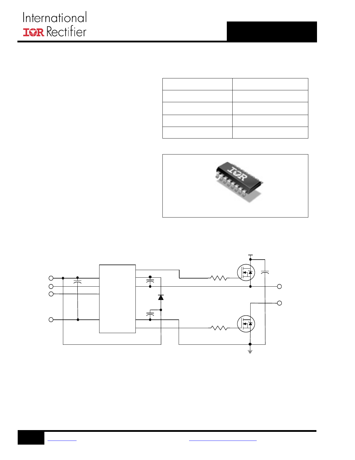
Typical Connection Diagram
(Refer to Lead Assignments for correct pin configuration). This/These
diagram(s) show electrical connections only. Please refer to our
Application Notes and Design Tips for proper circuit board layout.
2181
O
O
Vcc
HIN
LIN
COM
HO
LO
Up to 600V
Vcc
LIN
HIN
AUIRS21814
TO
LOAD
Vss
Vss
n
m(s) show
o our
oper
V
B
V
S
AUIRS2191S
2
www.irf.com
© 2012 International Rectifier
Submit Datasheet Feedback
November 18, 2013
Table of Contents
Page
Description
3
Qualification Information
4
Absolute Maximum Ratings
5
Recommended Operating Conditions
5
Static Electrical Characteristics
6
Dynamic Electrical Characteristics
6
Functional Block Diagram
7
Input/Output Pin Equivalent Circuit Diagram
8
Lead Definitions
9
Lead Assignments
9
Timing diagram
10
Parameter Temperature Trends
11, 13
Package Details
14, 15
Part Marking Information
16
Ordering Information
16
Important Notice
17

AUIRS2191S
3
www.irf.com
© 2012 International Rectifier
Submit Datasheet Feedback
November 18, 2013
Description
The AUIRS2191S is a high power, high voltage, high speed power MOSFET and IGBT driver with independent high and low side
referenced output channels, designed for Automotive AC/DC and DC/DC converter applications. Logic inputs are compatible with
standard CMOS or LSTTL output, down to 3.3V logic. The output drivers feature a high pulse current buffer stage designed for
minimum driver cross-conduction. Propagation delays are matched to simplify use in high frequency applications. The floating
channel can be used to drive an N-channel power MOSFET or IGBT in the high side configuration which operates up to 600V.
Proprietary HVIC and latch immune CMOS technologies enable ruggedized monolithic construction.
AUIRS2191S
4
www.irf.com
© 2012 International Rectifier
Submit Datasheet Feedback
November 18, 2013
Qualification Information
†
Qualification Level
Automotive
(per AEC-Q100
††
)
Comments: This family of ICs has passed an Automotive
qualification. IR’s Industrial and Consumer qualification
level is granted by extension of the higher Automotive
level.
Moisture Sensitivity Level
MSL3
††
260°C
(per IPC/JEDEC J-STD-020)
ESD
Machine Model
Class M1 (100V)
(per AEC-Q100-003)
Human Body Model
Class H1B (1000V)
(per AEC-Q100-002)
Charged Device Model
Class C4 (1000V)
(per AEC-Q100-011)
IC Latch-Up Test
Class II Level A
(per AEC-Q100-004)
RoHS Compliant
Yes
†
Qualification standards can be found at International Rectifier’s web site
http://www.irf.com/
†† Higher MSL ratings may be available for the specific package types listed here. Please contact your
International Rectifier sales representative for further information.
AUIRS2191S
5
www.irf.com
© 2012 International Rectifier
Submit Datasheet Feedback
November 18, 2013
Absolute Maximum Ratings
Absolute maximum ratings indicate sustained limits beyond which permanent damage to the device may occur. These are stress
ratings only, functional operation of the device at these or any other condition beyond those indicated in the “Recommended
Operating Condition” is not implied. Exposure to absolute maximum-rated conditions for extended periods may affect device
reliability. All voltage parameters are absolute voltages referenced to COM unless otherwise stated in the table. The thermal
resistance and power dissipation ratings are measured under board mounted and still air conditions.
Symbol
Definition
Min
Max
Units
V
B
High side floating supply voltage
-0.3
620
V
V
S
High side floating supply offset voltage
V
B
– 20
V
B
+ 0.3
V
HO
High side floating output voltage
V
S
– 0.3
V
B
+ 0.3
V
CC
Low side fixed supply voltage
-0.3
20
V
LO
Low-side output voltage
-0.3
V
CC
+ 0.3
V
IN
Logic input voltage (HIN & LIN)
V
SS
– 0.3
V
CC
+ 0.3
V
SS
Logic ground
V
CC
– 20
V
CC
+ 0.3
dV
S
/dt
Allowable V
S
offset supply transient
---
50
V/ns
P
D
Package power dissipation @ T
A
≤+25 ºC
---
1.0
W
R
ΘJA
Thermal resistance, junction to ambient
---
100
ºC/W
T
J
Junction temperature
---
150
ºC
T
S
Storage temperature
-55
150
T
L
Lead temperature (soldering, 10 seconds)
---
300
Recommended Operating Conditions
The input/output logic timing diagram is shown in Figure 1. For proper operation the device should be used within the
recommended conditions. The VS, VSS, and COM offset ratings are tested with all supplies biased at 15V differential.
Symbol
Definition
Min
Max
Units
V
B
High side floating supply absolute voltage
V
S
+ 10
V
S
+ 20
V
V
S
High side floating supply offset voltage
†
600
V
HO
High side floating output voltage
V
S
V
B
V
CC
Low side fixed supply voltage
10
20
V
LO
Low side output voltage
0
V
CC
V
IN
Logic input voltage (HIN & LIN)
V
SS
V
CC
V
SS
Logic ground
-5
5
T
A
Ambient temperature
-40
125
ºC
†
Logic operation for V
S
of –5 V to 600 V. Logic state held for V
S
of –5 V to –V
BS
.
(Please refer to Design Tip DT97-3 for more details)
AUIRS2191S
6
www.irf.com
© 2012 International Rectifier
Submit Datasheet Feedback
November 18, 2013
Static Electrical Characteristics
Unless otherwise noted, these specifications apply for an operating junction temperature range of -40°C
≤ Tj ≤ 125°C with bias
conditions of V
BIAS
(VCC or VBS) = 15V. The VIN, VTH parameters are referenced to VSS and are applicable to all logic input
leads: HIN and LIN. The VO parameters are referenced to COM and are applicable to the respective output leads: HO or LO.
Symbol
Definition
Min
Typ
Max
Unit
s
Test Conditions
V
IH
Logic “1” input voltage
2.5
---
---
V
V
CC
= 9.8V – 20V
V
IL
Logic “0” input voltage
---
---
0.8
V
OH 2mA
High level output voltage, V
BIAS
-V
O
---
---
2.5
I
o
= 2 mA
V
OH 20mA
High level output voltage, V
BIAS
-V
O
---
---
3.3
I
o
= 20 mA
V
OL
Low level output voltage, V
O
---
---
0.1
I
o
= 2 mA
I
LK
Offset supply leakage current
---
---
50
µA
V
B
= V
S
= 600 V
I
QBS
Quiescent V
BS
supply current
---
100
200
V
IN
= 0V or 3.3V
I
QCC
Quiescent V
CC
supply current
---
150
300
V
IN
= 0V or 3.3V
I
QBS18
Quiescent V
BS
supply current
---
180
300
V
IN
= 0V or 3.3V
V
BS
=18V
I
QCC18
Quiescent V
CC
supply current
---
300
450
V
IN
= 0V or 3.3V
V
CC
=18V
I
QBS20
Quiescent V
BS
supply current
---
850
1500
V
IN
= 0V or 3.3V
V
BS
=20V
I
QCC20
Quiescent V
CC
supply current
---
1500
2500
V
IN
= 0V or 3.3V
V
CC
=20V
I
IN+
Logic “1” input bias current
---
3.5
7
V
IN
= 3.3V
I
IN-
Logic “0” input bias current
---
---
1.0
V
IN
= 0V
V
BSUV+
V
BS
supply undervoltage positive going threshold
8.0
8.9
9.8
V
V
BSUV-
V
BS
supply undervoltage negative going
threshold
7.4
8.2
8.8
V
BSUVHYS
V
BS
supply undervoltage hysteresis
0.3
0.7
---
V
CCUV+
V
CC
supply undervoltage positive going threshold
8.0
8.9
9.8
V
CCUV-
V
CC
supply undervoltage negative going
threshold
7.4
8.2
9.0
V
CCUVHYS
V
CC
supply undervoltage hysteresis
0.3
0.7
---
I
O+
Output high short circuit pulsed current
(†)
2.6
3.5
---
A
V
O
= 0 V,
PW
≤ 10 μs,
Tj = 25°C
I
O-
Output low short circuit pulsed current
(†)
2.6
3.5
---
V
O
= 15 V,
PW
≤ 10 μs
Tj = 25°C
I
O+
Output high short circuit pulsed current
(†)
1.8
3.5
---
A
V
O
= 0 V,
PW
≤ 10 μs,
I
O-
Output low short circuit pulsed current
(†)
1.8
3.5
---
V
O
= 15 V,
PW
≤ 10 μs
(†)
Guaranteed by design
Dynamic Electrical Characteristics
Unless otherwise noted, these specifications apply for an operating junction temperature range of -40°C
≤ Tj ≤125°C with bias
conditions of V
BIAS
(VCC, VBS) = 15V, CL = 1000 pF. The dynamic electrical characteristics are measured using the test
definitions shown in Figure 3.
Symbol
Definition
Min
Typ
Max
Units
Test Conditions
t
ON
Turn-on propagation delay
50
90
175
ns
V
S
= 0V
AUIRS2191S
7
www.irf.com
© 2012 International Rectifier
Submit Datasheet Feedback
November 18, 2013
t
OFF
Turn-off propagation delay
50
90
175
V
S
= 0V or 600V
t
R
Turn-on rise time
5
15
60
t
F
Turn-off fall time
5
15
60
MT
Delay matching, HS & LS turn-on/off
---
---
25
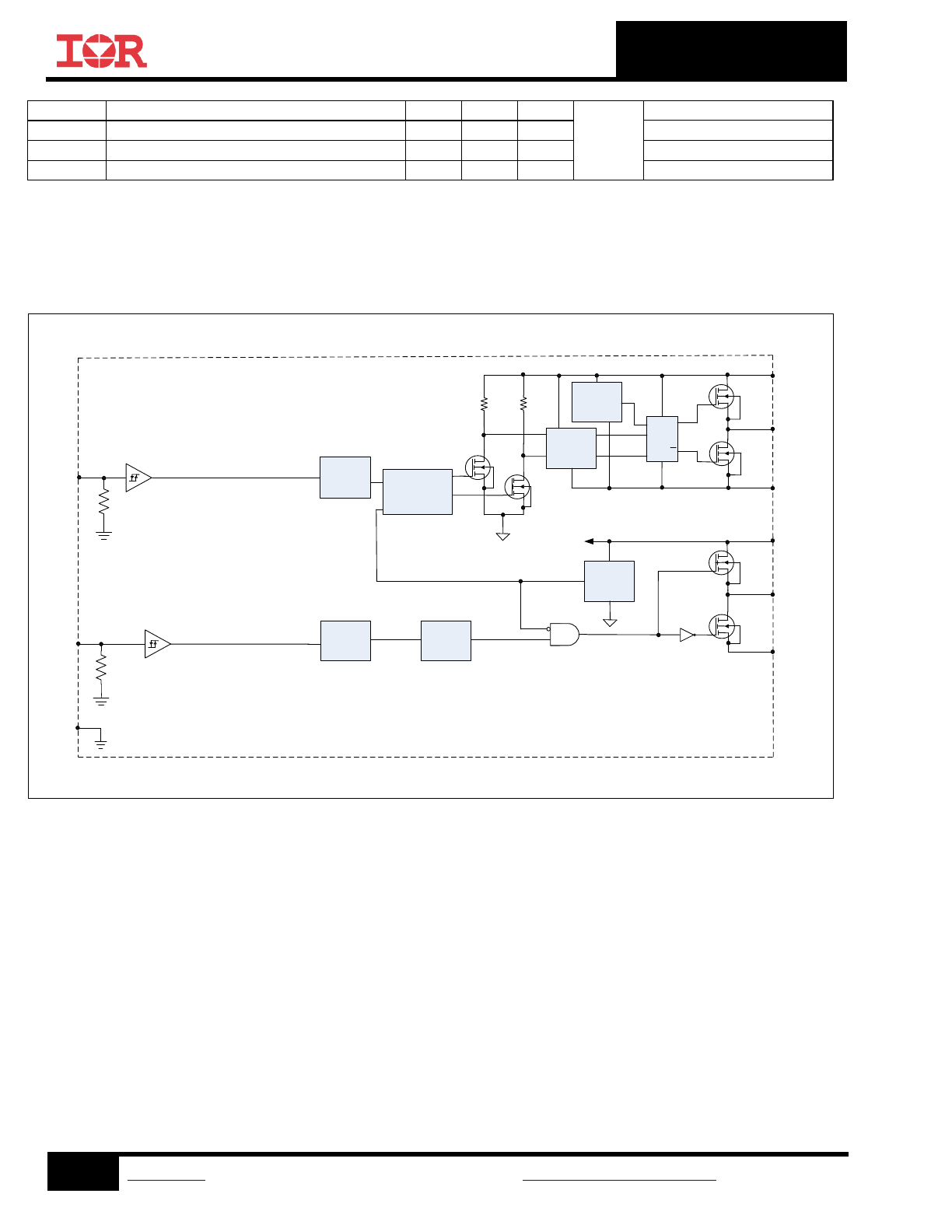
Functional Block Diagram
UV
DETECT
PULSE
GENERATOR
VSS/COM
LEVEL
SHIFT
PULSE
FILTER
HV
LEVEL
SHIFTER
Q
V
S
HO
V
B
S
R
R
VSS/COM
LEVEL
SHIFT
UV
DETECT
DELAY
V
CC
LO
COM
HIN
LIN
Q
V
SS
AUIRS2191S
8
www.irf.com
© 2012 International Rectifier
Submit Datasheet Feedback
November 18, 2013
Input/Output Pin Equivalent Circuit
Diagrams: AUIRS2191
V
CC
COM
LO
ESD
Diode
ESD
Diode
V
B
V
S
HO
ESD
Diode
ESD
Diode
20V
20V
600V
V
SS
20V
V
CC
V
SS
HIN
LIN
ESD
Diode
ESD
Diode
R
ESD
R
PD
AUIRS2191S
9
www.irf.com
© 2012 International Rectifier
Submit Datasheet Feedback
November 18, 2013
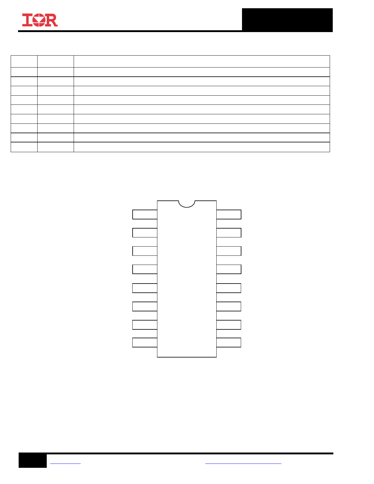
Lead Definitions: AUIRS2191
Pin#
Symbol
Description
1
VB
High-side floating supply
6
HIN
Logic inputs for high-side gate driver output (HO), in phase (referenced to V
SS
)
7
LIN
Logic inputs for low-side gate driver output (LO), in phase (referenced to V
SS
)
8
VSS
Low-side logic return
9
COM
Low-side return
11
LO
Low-side gate drive output
12
VCC
Low-side supply voltage
15
VS
High voltage floating supply return
16
HO
High-side gate drive output
Lead Assignments
16 Lead SOIC
16
15
14
13
VB
HO
1
2
3
4
VS
12
11
10
VCC
HIN
5
6
7
LO
LIN
9
8
COM
VSS
NC
NC
NC
NC
NC
NC
NC

AUIRS2191S
10
www.irf.com
© 2012 International Rectifier
Submit Datasheet Feedback
November 18, 2013
Application Information and Additional Details
HIN
LIN
HO
LO
Figure 1. Input/Output Timing Diagram
50%
10%
90%
t
r
LO
90%
10%
50%
t
f
t
on
t
off
HO
HIN
LIN
Figure 2. Switching Time Waveform Definitions
50%
10%
90%
MT
LO
HO
50%
HO
MT
LO
HIN
LIN
Figure 3. Delay Matching Waveform Definitions