
AUIRS2181(4)S
1
www.irf.com
© 2014 International Rectifier
Submit Datasheet Feedback
January 10, 2014
Features
• Floating channel designed for bootstrap operation
• Fully operational to +600 V
• Tolerant to negative transient voltage, dV/dt immune
• Gate drive supply range from 10 V to 20 V
• Undervoltage lockout for both channels
• 3.3 V and 5 V input logic compatible
• Matched propagation delay for both channels
• Logic and power ground +/- 5 V offset
• Lower di/dt gate driver for better noise immunity
• Output source/sink current capability (typical) 1.9 A /2.3 A
• Leadfree, RoHS compliant
• Automotive qualified*
Typical Applications
• Piezo/ common rail Injection
• Starter/Alternator
• Electric Power Steering
• Fan and compressor
Product Summary
Topology
High and Low Side Driver
V
OFFSET
≤ 600 V
V
OUT
10 V – 20 V
I
o+
& I
o-
(typical)
1.9 A &2.3 A
t
ON
& t
OFF
(typical)
160 ns & 200 ns
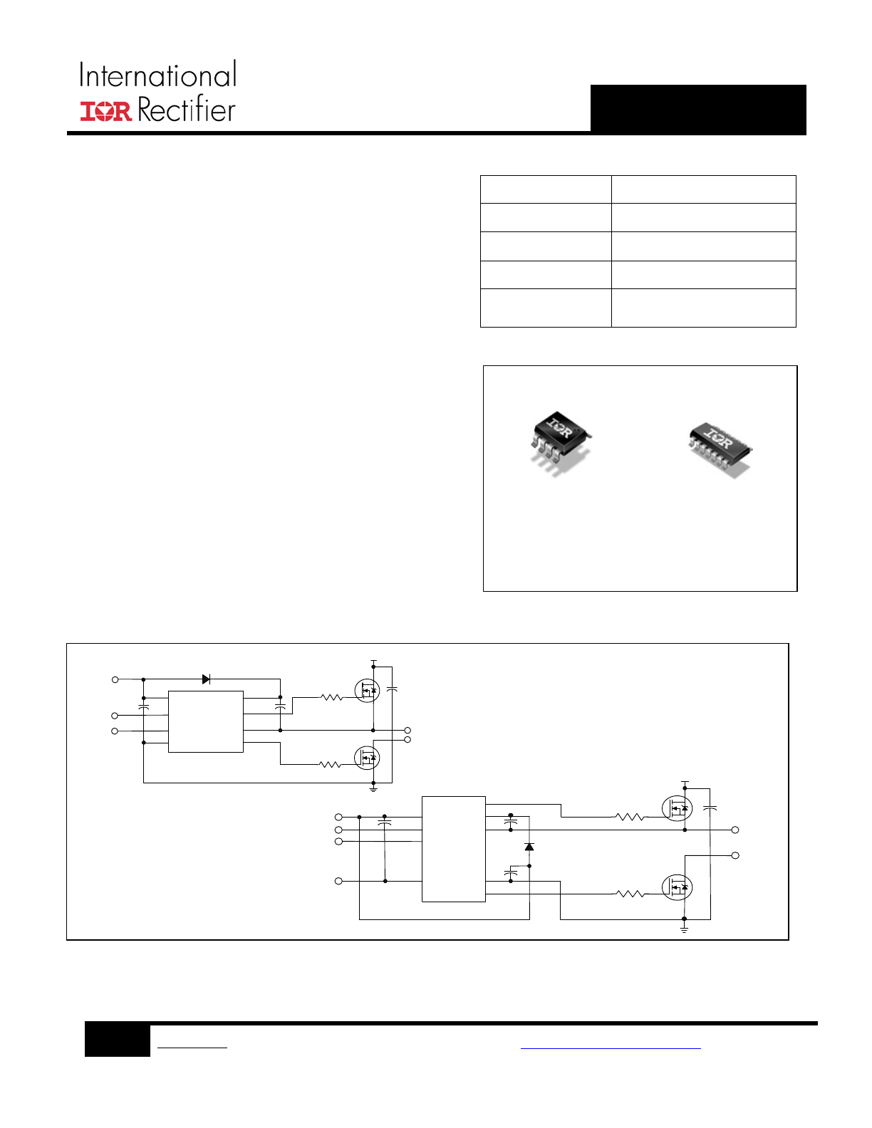
Package Options
Typical Connection
8-Lead SOIC 14-Lead SOIC
AUIRS2181S Narrow Body
AUIRS21814S
Vcc
HIN
LIN
COM
HO
LO
Up to 600V
Vcc
HIN
LIN
AUIRS2181
TO
LOAD
Vcc
HIN
LIN
COM
HO
LO
Up to 600V
Vcc
LIN
HIN
AUIRS21814
TO
LOAD
Vss
Vss
(Refer to Lead Assignments for correct pin
configuration). This/These diagram(s) show
electrical connections only. Please refer to our
Application Notes and Design Tips for proper
circuit board layout.
V
B
V
S
V
B
V
S
AUIRS2181(4)S
2
www.irf.com
© 2014 International Rectifier
Submit Datasheet Feedback
January 10, 2014
Ordering Information
Base Part Number
Package Type
Standard Pack
Complete Part Number
Form
Quantity
AUIRS2181S
SOIC8
Tube/Bulk
95
AUIRS2181S
Tape and Reel
2500
AUIRS2181STR
AUIRS21814S
SOIC14N
Tube/Bulk
55
AUIRS21814S
Tape and Reel
2500
AUIRS21814STR
AUIRS2181(4)S
3
www.irf.com
© 2014 International Rectifier
Submit Datasheet Feedback
January 10, 2014
Description
The AUIRS2181(4)(S) are high voltage, high speed power MOSFET and IGBT drivers with independent high
and low-side referenced output channels. Proprietary HVIC and latch immune CMOS technologies enable
ruggedized monolithic construction. The logic input is compatible with standard CMOS or LSTTL output,
down to 3.3 V logic. The output drivers feature a high pulse current buffer stage designed for minimum driver
cross-conduction. The floating channel can be used to drive an N-channel power MOSFET or IGBT in the
high-side configuration which operates up to 600 V.
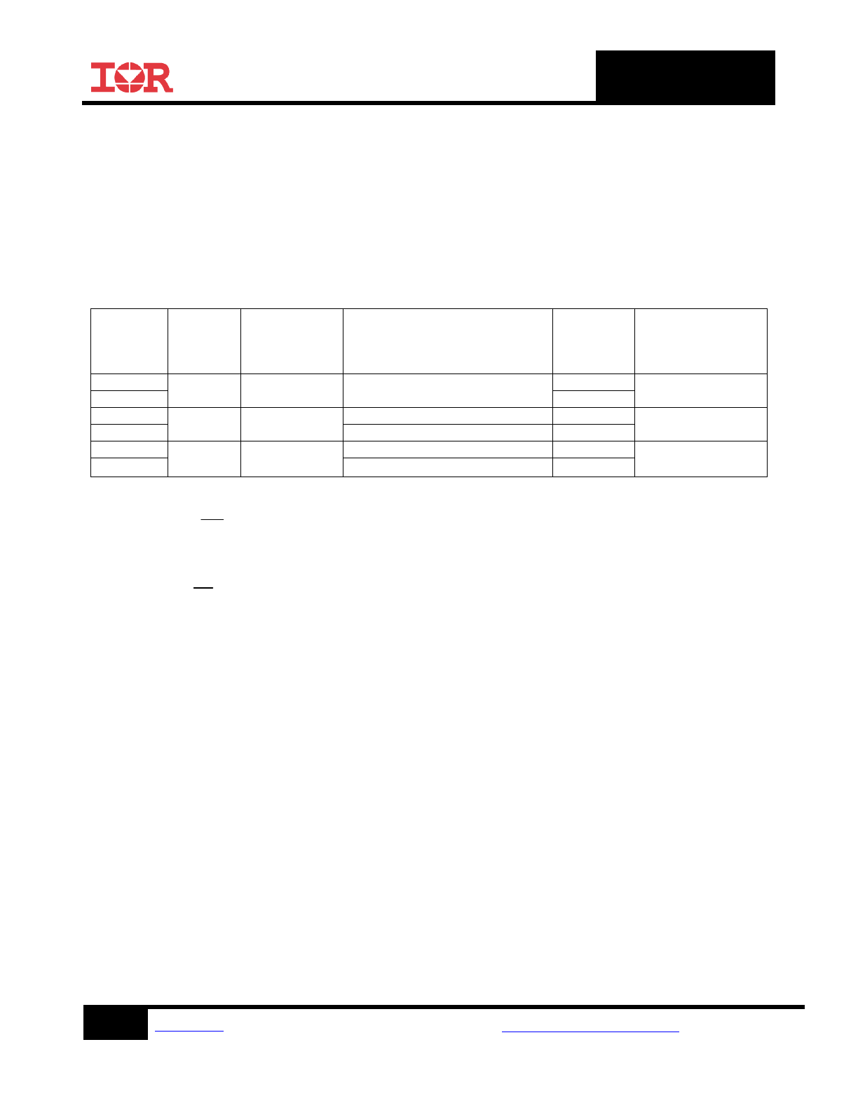
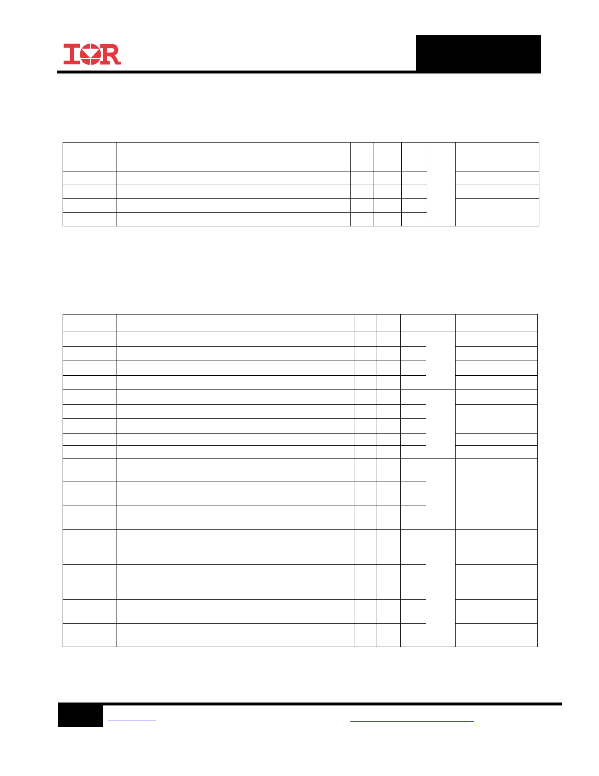
Feature Comparison: AUIRS2181/AUIRS2183/AUIRS2184
Part
Input
Logic
Cross-
Conduction
Prevention
logic
Dead-Time
Ground
Pins
Ton/Toff
2181
HIN/LIN
no
none
COM
160/200 ns
21814
V
SS
/COM
2183
HIN/LIN
yes
Internal 500ns
COM
160/200 ns
21834
Programmable 0.4 – 5 us
V
SS
/COM
2184
IN/SD
yes
Internal 500ns
COM
600/230 ns
21844
Programmable 0.4 – 5 us
V
SS
/COM
AUIRS2181(4)S
4
www.irf.com
© 2014 International Rectifier
Submit Datasheet Feedback
January 10, 2014
Absolute Maximum Ratings
Absolute Maximum Ratings indicate sustained limits beyond which damage to the device may occur. All
voltage parameters are absolute voltages referenced to COM lead. Stresses beyond those listed under "
Absolute Maximum Ratings" may cause permanent damage to the device. These are stress ratings only;
and functional operation of the device at these or any other condition beyond those indicated in the
“Recommended Operating Conditions” is not implied. Exposure to absolute-maximum-rated conditions for
extended periods may affect device reliability. The thermal resistance and power dissipation ratings are
measured under board mounted and still air conditions. Ambient temperature (T
A
) is 25°C, unless otherwise
specified.
Symbol
Definition
Min
Max
Units
V
B
High-side floating absolute voltage
-0.3
625
V
V
S
High-side floating supply offset voltage
V
B
- 25
V
B
+ 0.3
V
HO
High-side floating output voltage
V
S
- 0.3
V
B
+ 0.3
V
CC
Low-side and logic fixed supply voltage
-0.3
20
(†)
V
LO
Low-side output voltage
-0.3
V
CC
+ 0.3
V
IN
Logic input voltage (HIN &LIN)
V
SS
-0.3
V
CC
+ 0.3
V
SS
Logic ground (AUIRS21814(S) only)
V
CC
- 20
V
CC
+ 0.3
dV
S
/dt
Allowable offset supply voltage transient
—
50
V/ns
P
D
Package power dissipation @ TA ≤ 25°C
(8 lead SOIC)
—
0.625
W
(14 lead SOIC)
—
1.0
Rth
JA
Thermal resistance, junction to ambient
(8 lead SOIC)
—
200
°C/W
(14 lead SOIC)
—
120
T
J
Junction temperature
—
150
°C
T
S
Storage temperature
-50
150
T
L
Lead temperature (soldering, 10 seconds)
—
300
† All supplies are fully tested at 25 V and an internal 20 V clamp exists for each supply.
Recommended Operating Conditions
The input/output logic timing diagram is shown in figure 1. For proper operation the device should be used
within the recommended conditions. The V
S
and V
SS
offset rating are tested with all supplies biased at 15 V
differential.
†† Logic operational for V
S
of -5 V to +600 V. Logic state held for V
S
of -5 V to –V
BS
. (Please refer to the
Design Tip DT97-3 for more details).
Symbol
Definition
Min
Max
Units
V
B
High-side floating supply absolute voltage
V
S
+10
V
S
+20
V
V
S
High-side floating supply offset voltage
(††)
600
V
HO
High-side floating output voltage
V
S
V
B
V
CC
Low-side and logic fixed supply voltage
10
20
V
LO
Low-side output voltage
0
V
CC
V
IN
Logic input voltage
V
SS
V
CC
DT
Programmable deadtime pin voltage
V
SS
V
CC
V
SS
Logic ground
-5
5
T
A
Ambient temperature
-40
125
°C
AUIRS2181(4)S
5
www.irf.com
© 2014 International Rectifier
Submit Datasheet Feedback
January 10, 2014
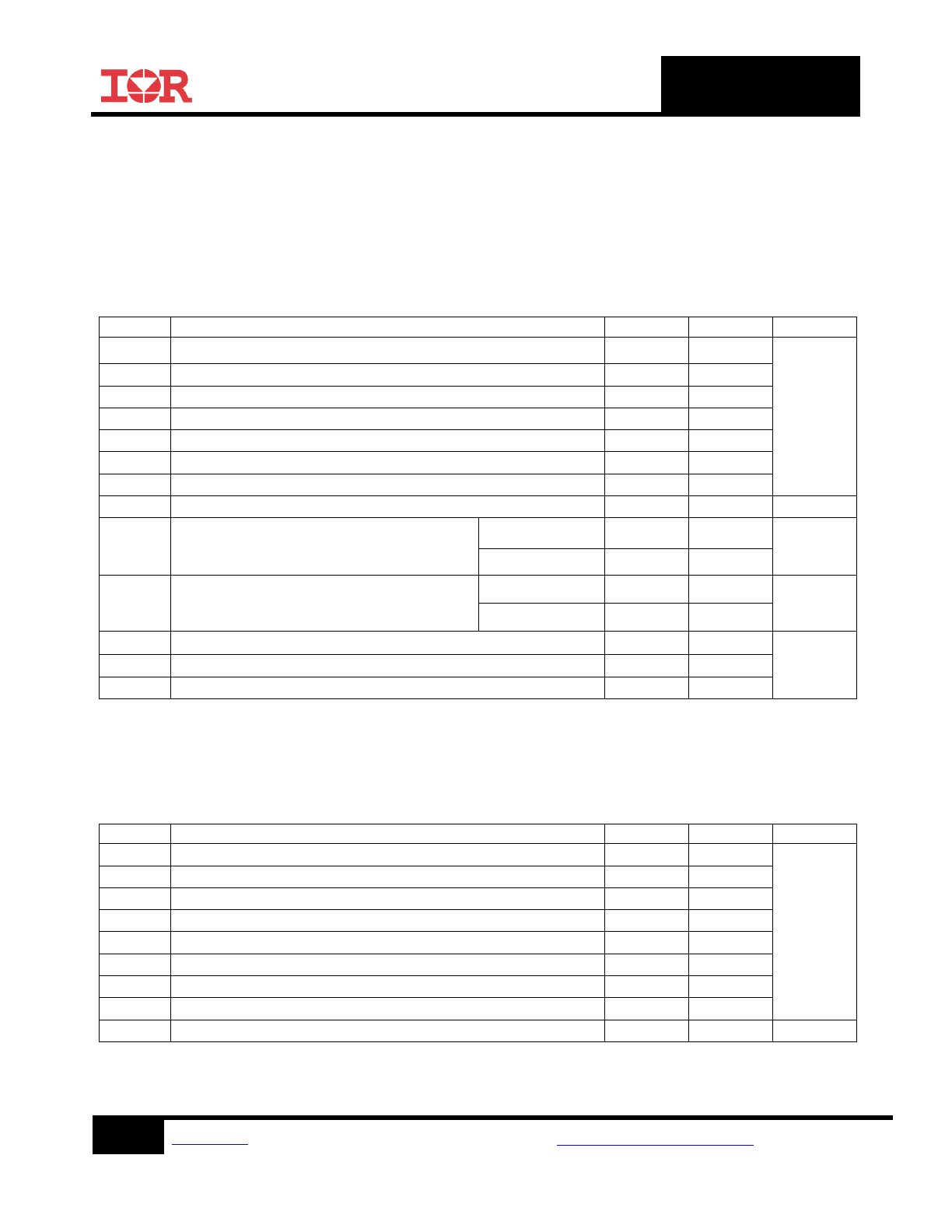
Dynamic Electrical Characteristics
Unless otherwise noted, these specifications apply for an operating junction temperature range of -40°C
≤ Tj
≤ 125°C with bias conditions of V
BIAS
(V
CC
, V
BS
) = 15 V, V
SS
= COM, C
L
= 1000 pF.
Symbol
Definition
Min Typ Max Units Test Conditions
t
on
Turn-on propagation delay
—
160 270
ns
V
S
= 0 V
t
off
Turn-off propagation delay
—
200 330
V
S
= 0 V or 600 V
MT
Delay matching, HS & LS turn-on/off
—
—
35
t
r
Turn-on rise time
—
15
60
V
S
= 0 V
t
f
Turn-off fall time
—
15
35
Static Electrical Characteristics
Unless otherwise noted, these specifications apply for an operating junction temperature range of -40°C
≤ Tj
≤ 125°C with bias conditions of V
BIAS
(V
CC
, V
BS
) = 15 V, V
SS
= COM. The V
IL,
V
IH
and I
IN
parameters are
referenced to V
SS
/COM and are applicable to the respective input leads: HIN and LIN. The V
O,
I
O
and Ron
parameters are referenced to COM and are applicable to the respective output leads: HO and LO.
(†) Guaranteed by design
(††) I
O+
and I
O-
decrease with rising temperature
Symbol
Definition
Min Typ Max Units Test Conditions
V
IH
Logic “1” input voltage
2.5 —
—
V
V
CC
= 10 V to 20 V
V
IL
Logic “0” input voltage
—
—
0.8
V
CC
= 10 V to 20 V
V
OH
High level output voltage, V
BIAS
-
V
O
—
—
1.4
I
O
= 0 mA
V
OL
Low level output voltage, V
O
—
—
0.2
I
O
= 20 mA
I
LK
Offset supply leakage current
—
—
50
µA
V
B
=
V
S
= 600 V
I
QBS
Quiescent V
BS
supply current
15
60 150
V
IN
= 0 V or 5 V
I
QCC
Quiescent V
CC
supply current
15 120 240
I
IN+
Logic “1” input bias current
—
25
60
V
IN
= 5 V
I
IN-
Logic “0” input bias current
—
—
5.0
V
IN
= 0 V
V
CCUV+
V
BSUV+
V
CC
and V
BS
supply undervoltage positive
going threshold
8.0 8.9 9.8
V
V
CCUV-
V
BSUV-
V
CC
and V
BS
supply undervoltage negative
going threshold
7.4 8.2 9.0
V
CCUVH
V
BSUVH
V
CC
and V
BS
supply undervoltage Hysteresis
0.3 0.7
—
I
O25+
(†)
Output high short circuit pulsed current
1.4 1.9
—
A
V
O
= 0V,
PW ≤ 10us,
T
J
= 25°C
I
O25-
(†)
Output low short circuit pulsed current
1.8 2.3
—
V
O
= 15V,
PW ≤ 10us,
T
J
= 25°C
I
O+
(†)(††)
Output high short circuit pulsed current
1.2 —
—
V
O
= 0 V,
PW ≤ 10 us
I
O-
(†)(††)
Output low short circuit pulsed current
1.5 —
—
V
O
= 15 V,
PW ≤ 10 us
AUIRS2181(4)S
6
www.irf.com
© 2014 International Rectifier
Submit Datasheet Feedback
January 10, 2014
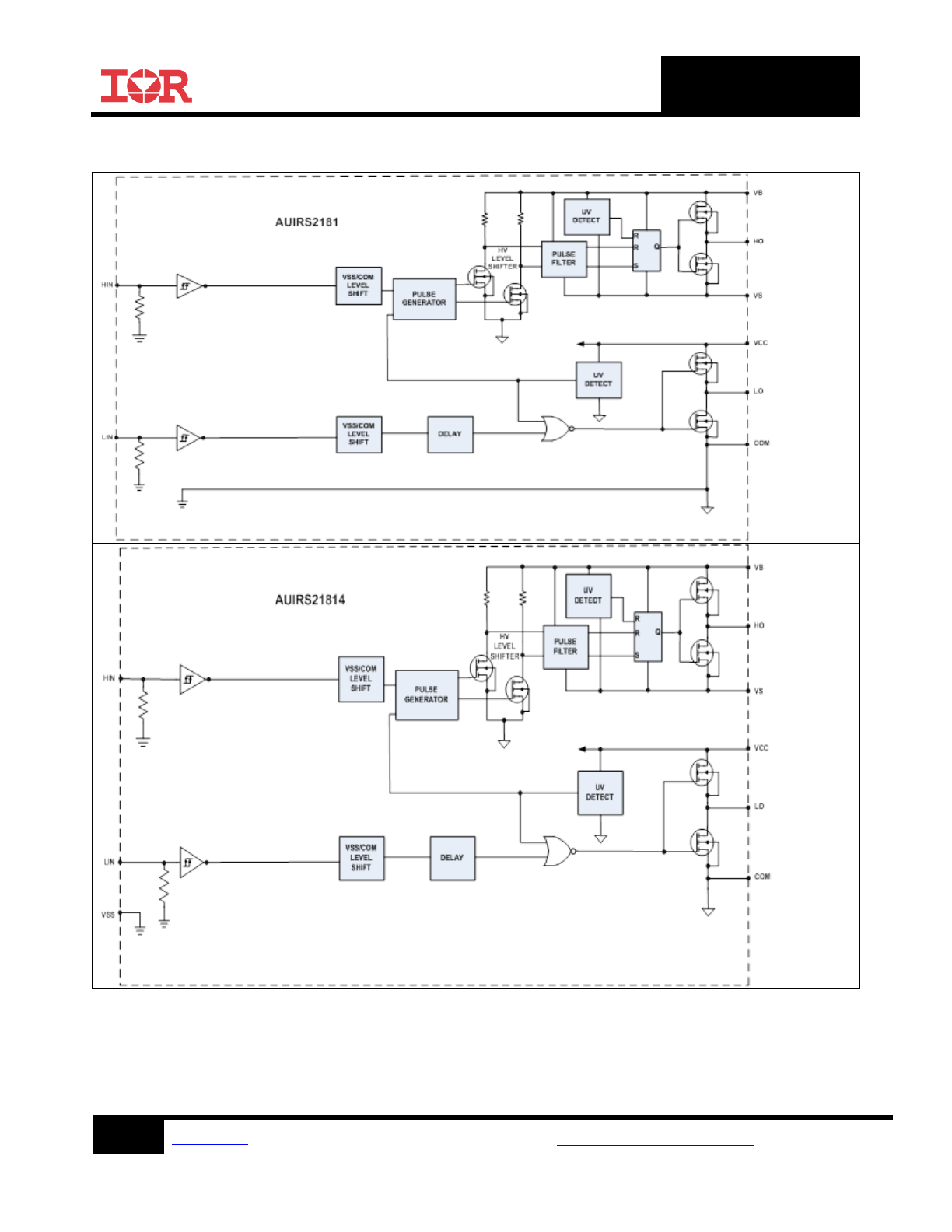
Functional Block Diagrams: AUIRS2181, AUIRS21814
AUIRS2181(4)S
7
www.irf.com
© 2014 International Rectifier
Submit Datasheet Feedback
January 10, 2014
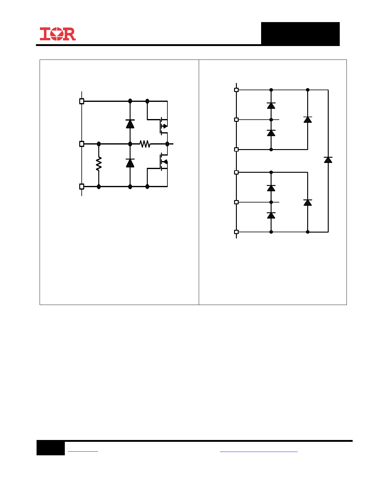
Input/Output Pin Equivalent Circuit
Diagrams: AUIRS2181S
V
CC
V
SS
HIN
LIN
ESD
Diode
ESD
Diode
R
ESD
R
PD
V
CC
COM/V
SS
LO
ESD
Diode
ESD
Diode
V
B
V
S
HO
ESD
Diode
ESD
Diode
20V
20V
600V
AUIRS2181(4)S
8
www.irf.com
© 2014 International Rectifier
Submit Datasheet Feedback
January 10, 2014
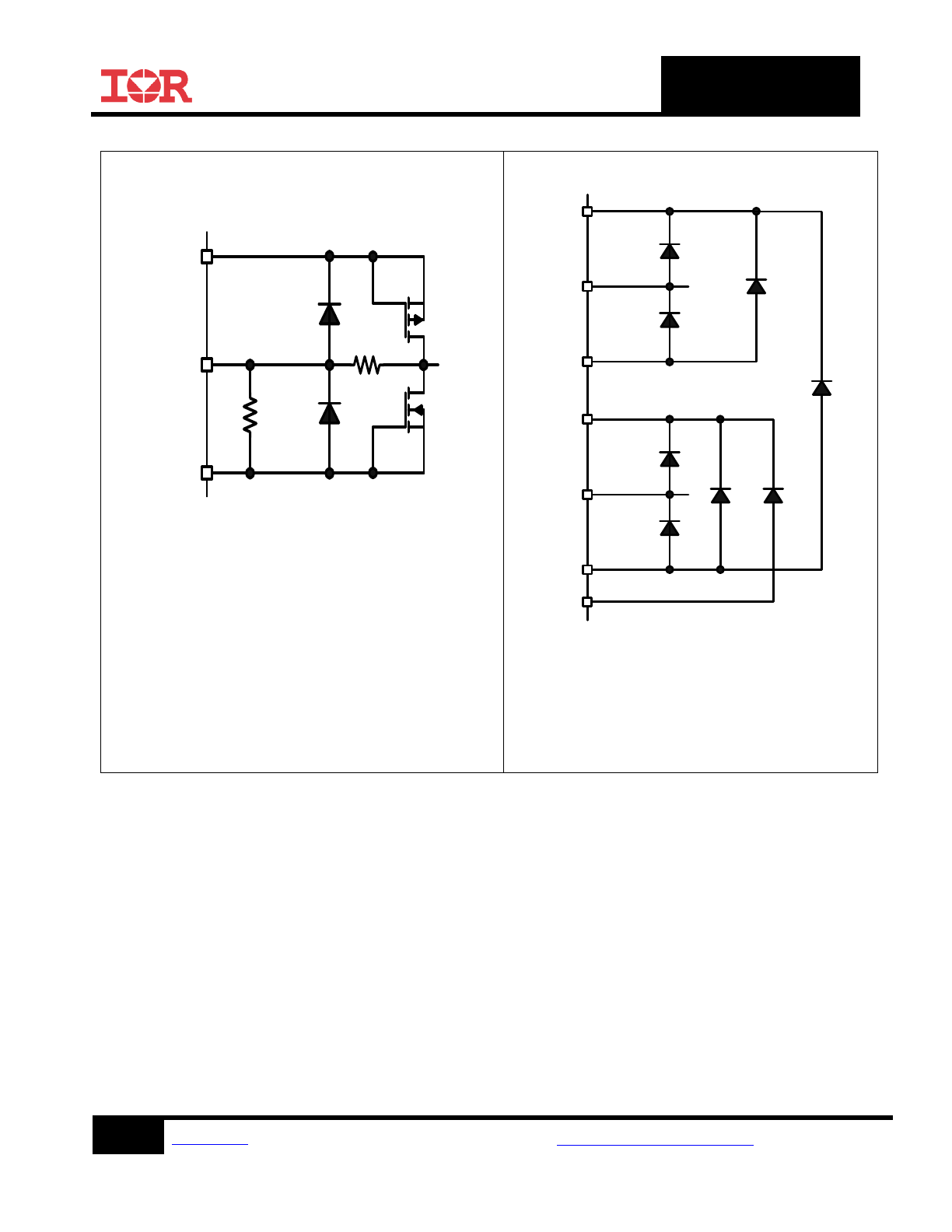
Input/Output Pin Equivalent Circuit
Diagrams: AUIRS21814S
V
CC
V
SS
HIN
LIN
ESD
Diode
ESD
Diode
R
ESD
R
PD
V
CC
COM
LO
ESD
Diode
ESD
Diode
V
B
V
S
HO
ESD
Diode
ESD
Diode
20V
20V
600V
V
SS
20V
AUIRS2181(4)S
9
www.irf.com
© 2014 International Rectifier
Submit Datasheet Feedback
January 10, 2014
Lead Definitions: AUIRS2181(4)S
Symbol
Description
HIN
Logic input for high-side gate driver output (HO), in phase
LIN
Logic input for low-side driver output (LO), in phase
V
SS
Logic ground (AUIRS21814 only)
V
B
High-side floating supply
HO
High-side gate drive output
V
S
High-side floating supply return
V
CC
Low-side and logic fixed supply
LO
Low-side gate drive output
COM
Low-side return
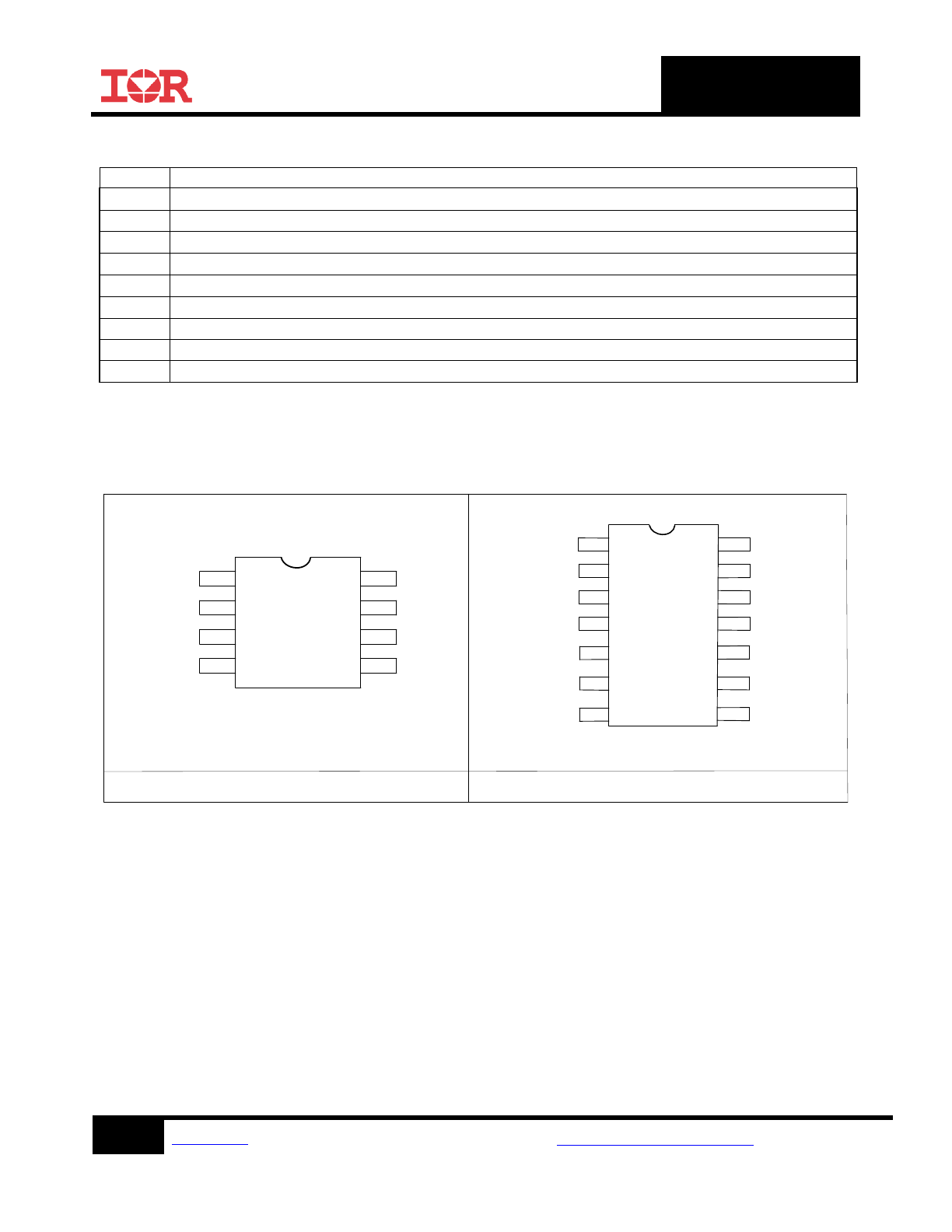
Lead Assignments: AUIRS2181(4)S
8 Lead SOIC
8
7
6
5
V
CC
V
B
HIN
1
2
3
4
V
S
HO
LO
LIN
COM
14
13
12
V
CC
V
B
HIN
1
V
S
HO
LIN
COM
4
5
7
6
2
3
LO
V
SS
11
10
9
8
AUIRS2181S
AUIRS21814S
14 Lead SOIC
Narrow Body

AUIRS2181(4)S
10
www.irf.com
© 2014 International Rectifier
Submit Datasheet Feedback
January 10, 2014
Application Information and Additional Details
HIN
LIN
HO
LO
50%
10%
90%
t
r
HIN
HO
90%
10%
50%
t
f
t
on
t
off
LIN
LO
50%
10%
90%
MT
LIN
LO
HO
50%
HO
MT
HIN
LO
Figure 1. Input/Output Timing Diagram
Figure 2. Switching Time Waveform Definitions
Figure 3. Delay Matching Waveform Definitions