
1
www.irf.com
© 2014 International Rectifier
Submit Datasheet Feedback
July 15, 2014
AUIRS211(7,8)S
SINGLE CHANNEL DRIVER
Features
Floating channel designed for bootstrap operation
Fully operational to +600 V
Tolerant to negative transient voltage - dV/dt immune
Gate drive supply range from 10 V to 20 V
Undervoltage lockout
CMOS Schmitt-triggered inputs with pull-down
(AUIRS2117) or pull-up (AUIRS2118)
Output in phase with input (AUIRS2117) or out of
Phase with input (AUIRS2118)
Leadfree, RoHS compliant
Automotive qualified*
Typical Applications
Direct/Piezo injection
BLDC Motor Drive
MOSFET and IGBT drivers
Product Summary
Topology
Single High Side
V
OFFSET
≤ 600 V
V
OUT
10 V
– 20 V
I
o+
& I
o-
(typical)
290 mA & 600 mA
t
ON
& t
OFF
(typical)
140 ns & 140 ns
Package Options
8-Lead SOIC
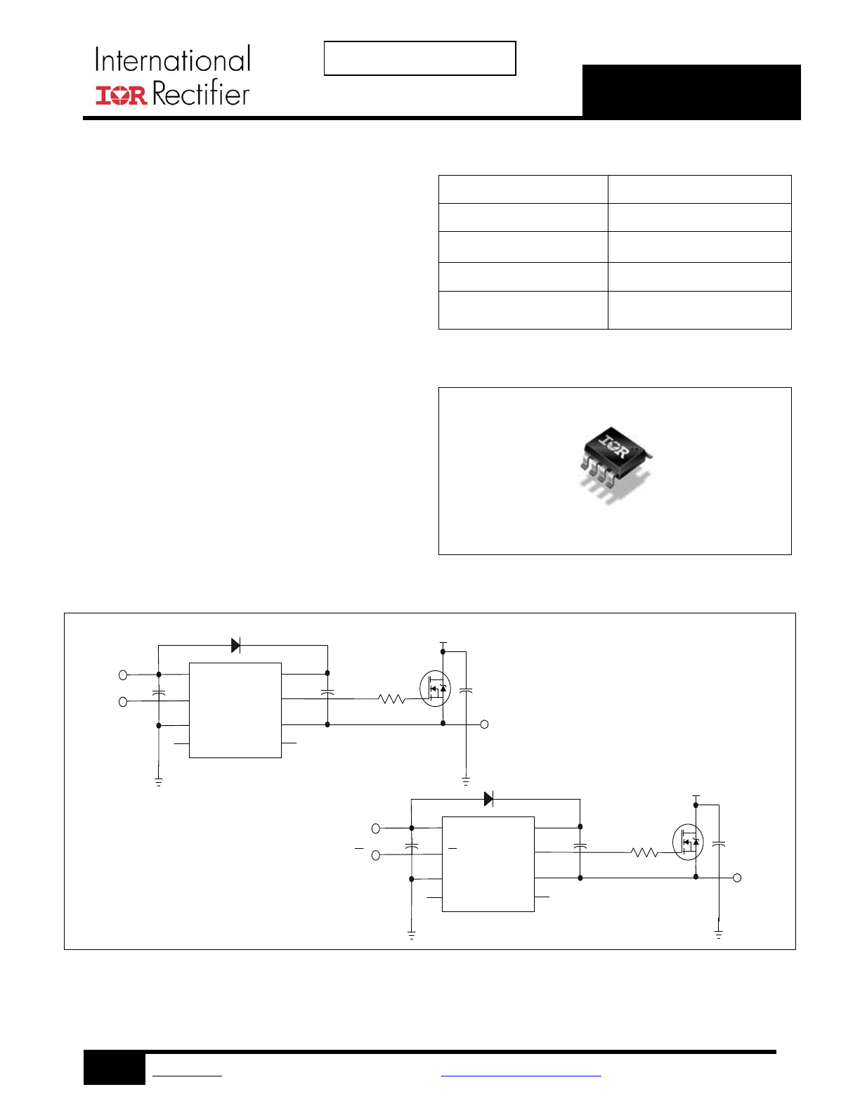
Typical Connection Diagram
Automotive Grade
(Refer to Lead Assignments for correct pin configuration). This/These
diagram(s) show electrical connections only. Please refer to our
Application Notes and Design Tips for proper circuit board layout.
Vcc
IN
COM
HO
Up to 600 V
Vcc
IN
AUIRS2117
TO
LOAD
V
B
V
S
Vcc
IN
COM
HO
Up to 600 V
Vcc
IN
AUIRS2118
TO
LOAD
V
B
V
S
AUIRS211(7,8)S
2
www.irf.com
© 2014 International Rectifier
Submit Datasheet Feedback
July 15, 2014
Table of Contents
Page
Description
3
Qualification Information
4
Absolute Maximum Ratings
5
Recommended Operating Conditions
5
Static Electrical Characteristics
6
Dynamic Electrical Characteristics
6
Functional Block Diagram
7
Input/Output Pin Equivalent Circuit Diagram
8
Lead Definitions
9
Lead Assignments
9
Application Information and Additional Details
10-13
Parameter Temperature Trends
13-16
Package Details
17
Tape and Reel Details
18
Part Marking Information
19
Ordering Information
20
AUIRS211(7,8)S
3
www.irf.com
© 2014 International Rectifier
Submit Datasheet Feedback
July 15, 2014
Description
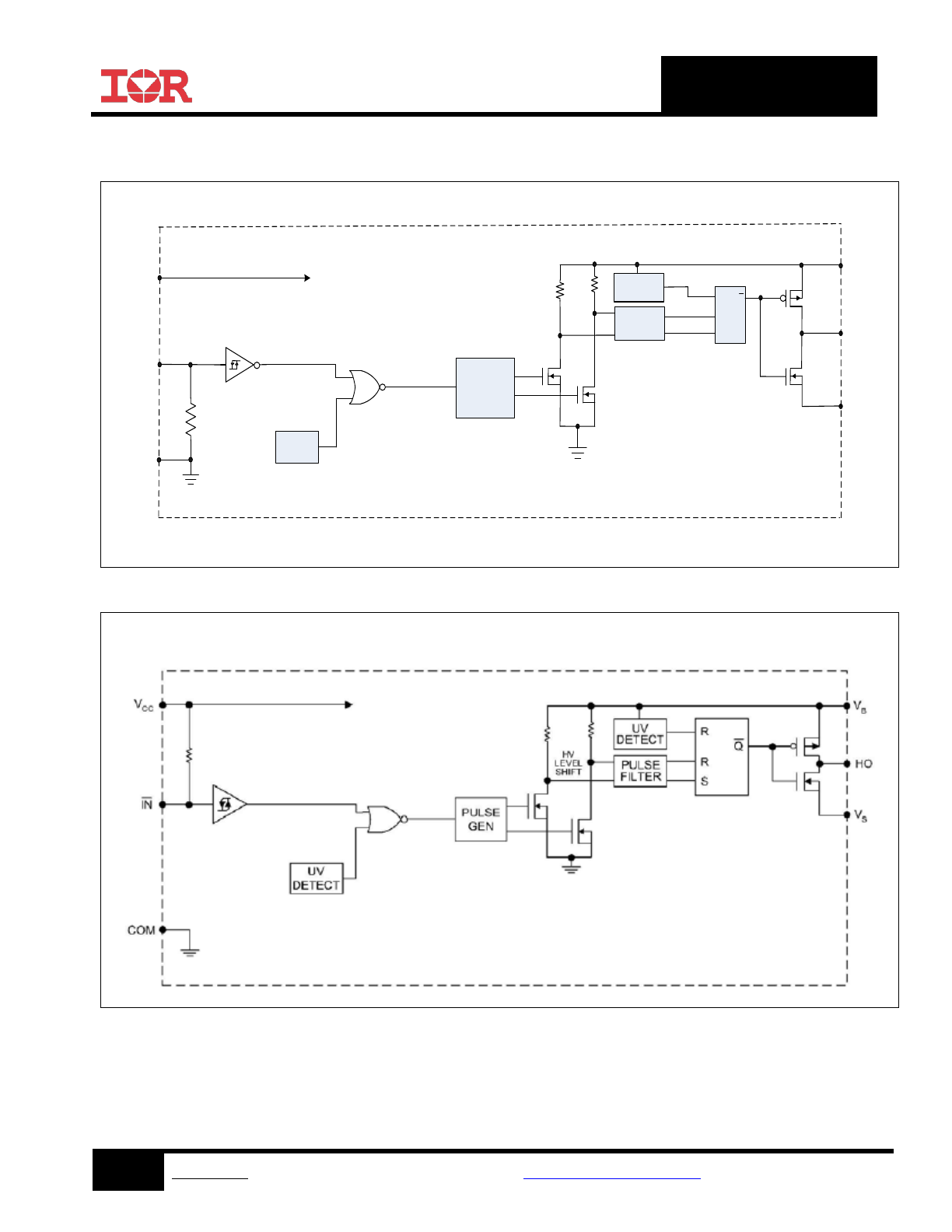
The AUIRS2117S/AUIRS2118S are high voltage, high speed power MOSFET and IGBT drivers. Proprietary
HVIC and latch immune CMOS technologies enable ruggedized monolithic construction. The logic input is
compatible with standard CMOS outputs. The output drivers feature a high pulse current buffer stage. The
floating channel can be used to drive an N-channel power MOSFET or IGBT in the high- side or low-side
configuration which operates up to 600 V.
Qualification Information
†
Qualification Level
Automotive
(per AEC-Q100)
Comments: This family of ICs has passed an Automotive
qualification.
IR’s Industrial and Consumer qualification
level is granted by extension of the higher Automotive
level.
Moisture Sensitivity Level
SOIC8N
MSL3
††
260°C
(per IPC/JEDEC J-STD-020)
ESD
Machine Model
Class M2 (Pass +/-200V)
(per AEC-Q100-003)
Human Body Model
Class H1B (Pass +/-1000V)
(per AEC-Q100-002)
Charged Device Model
Class C4 (Pass +/-1000V)
(per AEC-Q100-011)
IC Latch-Up Test
Class II, Level A
(per AEC-Q100-004)
RoHS Compliant
Yes
†
Qualification standards ca
n be found at International Rectifier’s web site
http://www.irf.com/
†† Higher MSL ratings may be available for the specific package types listed here. Please contact your
International Rectifier sales representative for further information.
AUIRS211(7,8)S
4
www.irf.com
© 2014 International Rectifier
Submit Datasheet Feedback
July 15, 2014
Absolute Maximum Ratings
Absolute Maximum Ratings indicate sustained limits beyond which damage to the device may occur. All voltage
parameters are absolute voltages referenced to COM lead. Stresses beyond those listed under "
Absolute Maximum Ratings" may cause permanent damage to the device. These are stress ratings only; and
functional operation of the device at these or any other condition beyond those indicated in the “Recommended
Operating Conditions” is not implied. Exposure to absolute-maximum-rated conditions for extended periods may
affect device reliability. The thermal resistance and power dissipation ratings are measured under board
mounted and still air conditions. Ambient temperature (T
A
) is 25°C, unless otherwise specified.
Recommended Operating Conditions
The input/output logic timing diagram is shown in Fig. 1. For proper operation the device should be used within
the recommended conditions. The V
S
offset rating is tested with all supplies biased at 15 V differential.
† Logic operational for V
S
of -5 V to +600 V. Logic state held for V
S
of -5 V to
– V
BS.
(Please refer to the Design Tip DT97-3 for more details).
Symbol
Definition
Min.
Max.
Units
V
B
High-side floating absolute voltage
-0.3
625
V
V
S
High-side floating supply offset voltage
V
B
- 25
V
B
+ 0.3
V
HO
High-side floating output voltage
V
S
- 0.3
V
B
+ 0.3
V
CC
Logic supply voltage
-0.3
25
V
IN
Logic input voltage
-0.3
V
CC
+ 0.3
dV
S
/dt
Allowable offset supply voltage transient (Fig. 2)
—
50
V/ns
P
D
Package power
dissipation @ TA ≤ 25°C
—
0.625
W
Rth
JA
Thermal resistance, junction to ambient
—
200
°C/W
T
J
Junction temperature
—
150
°C
T
S
Storage temperature
-55
150
T
L
Lead temperature (soldering, 10 seconds)
—
300
Symbol
Definition
Min
Max
Units
V
B
High-side floating supply absolute voltage
V
S
+10
V
S
+20
V
V
S
High-side floating supply offset voltage
†
600
V
HO
High-side floating output voltage
V
S
V
B
V
CC
Logic supply voltage
10
20
V
IN
Logic input voltage
0
V
CC
T
A
Ambient temperature
-40
125
°C

AUIRS211(7,8)S
5
www.irf.com
© 2014 International Rectifier
Submit Datasheet Feedback
July 15, 2014
Static Electrical Characteristics
Unless otherwise noted, these specifications apply for an operating junction temperature range of -40°C
≤ Tj ≤
125°C with bias conditions of V
BIAS
(V
CC
, V
BS
) = 15 V. The V
IL,
V
IH
and I
IN
parameters are referenced to COM. The
V
O
and I
O
parameters are referenced to COM and are applicable to the respective output leads: HO.
Dynamic Electrical Characteristics
Unless otherwise noted, these specifications apply for an operating junction temperature range of -40
°C ≤ Tj ≤
125°C with bias conditions of V
BIAS
(V
CC
, V
BS
) = 15 V, C
L
= 1000 pF. The dynamic electrical characteristics are
measured using the test circuit shown in Fig. 3.
Note: Please refer to figures in Parameter Temperature Trends section
Symbol
Definition
Min Typ Max Units
Test Conditions
V
IH
Logic “1” input voltage
AUIRS2117
9.5
—
—
V
AUIRS2118
V
IL
Logic “0” input voltage
AUIRS2117
—
—
6.0
AUIRS2118
V
OH
High level output voltage, V
BIAS
-
V
O
— 0.05 0.2
I
O
= 2 mA
V
OL
Low level output voltage, V
O
†
— 0.02 0.2
I
LK
Offset supply leakage current
—
—
50
µA
V
B
=
V
S
= 600 V
I
QBS
Quiescent V
BS
supply current
—
50
240
V
IN
= 0 V or V
CC
I
QCC
Quiescent V
CC
supply current
—
70
340
I
IN+
Logic “1” input bias current
AUIRS2117
—
20
40
V
IN
= V
CC
AUIRS2118
V
IN
= 0 V
I
IN-
Logic “0” input bias current
AUIRS2117
—
—
5.0
AUIRS2118
V
IN
= V
CC
V
BSUV+
V
BS
supply undervoltage positive going threshold
7.6
8.6
9.6
V
V
BSUV-
V
BS
supply undervoltage negative going threshold 7.2
8.2
9.2
V
CCUV+
V
CC
supply undervoltage positive going threshold 7.6
8.6
9.6
V
CCUV-
V
CC
supply undervoltage negative going threshold 7.2
8.2
9.2
I
O+
Output high short circuit pulsed current
200 290
—
mA
V
O
= 0 V,
V
IN
= Logic “1”
PW ≤ 10 µs
I
O-
Output low short circuit pulsed current
420 600
—
V
O
= 15 V,
V
IN
= Logic “0”
PW ≤ 10 µs
Symbol
Definition
Min
Typ
Max Units
Test Conditions
t
on
Turn-on propagation delay
—
140
225
ns
V
S
= 0 V
t
off
Turn-off propagation delay
—
140
225
V
S
= 600 V
t
r
Turn-on rise time
—
75
130
t
f
Turn-off fall time
—
25
65
AUIRS211(7,8)S
6
www.irf.com
© 2014 International Rectifier
Submit Datasheet Feedback
July 15, 2014
Functional Block Diagram: (AUIRS2117)
Functional Block Diagram: (AUIRS2118)
PULSE
GENERATOR
PULSE
FILTER
HV
LEVEL
SHIFTER
Q
V
S
HO
V
B
S
R
UV
DETECT
AUIRS2117
IN
V
CC
COM
UV
DETECT
R
AUIRS2118
AUIRS211(7,8)S
7
www.irf.com
© 2014 International Rectifier
Submit Datasheet Feedback
July 15, 2014
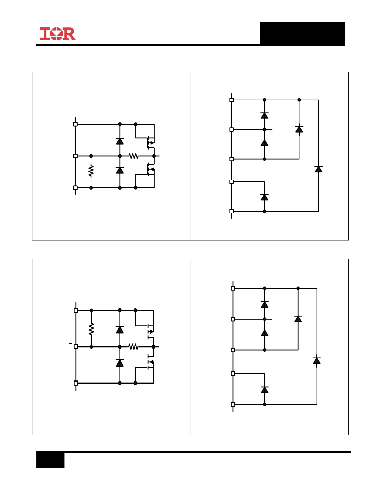
Input/Output Pin Equivalent Circuit
Diagrams: AUIRS2117S
V
CC
COM
IN
ESD
Diode
ESD
Diode
R
ESD
R
PD
V
CC
COM
V
B
V
S
HO
ESD
Diode
ESD
Diode
25V
25V
600V
Input/Output Pin Equivalent Circuit
Diagrams: AUIRS2118S
V
CC
COM
IN
ESD
Diode
ESD
Diode
R
ESD
R
PU
V
CC
COM
V
B
V
S
HO
ESD
Diode
ESD
Diode
25V
25V
600V
AUIRS211(7,8)S
8
www.irf.com
© 2014 International Rectifier
Submit Datasheet Feedback
July 15, 2014
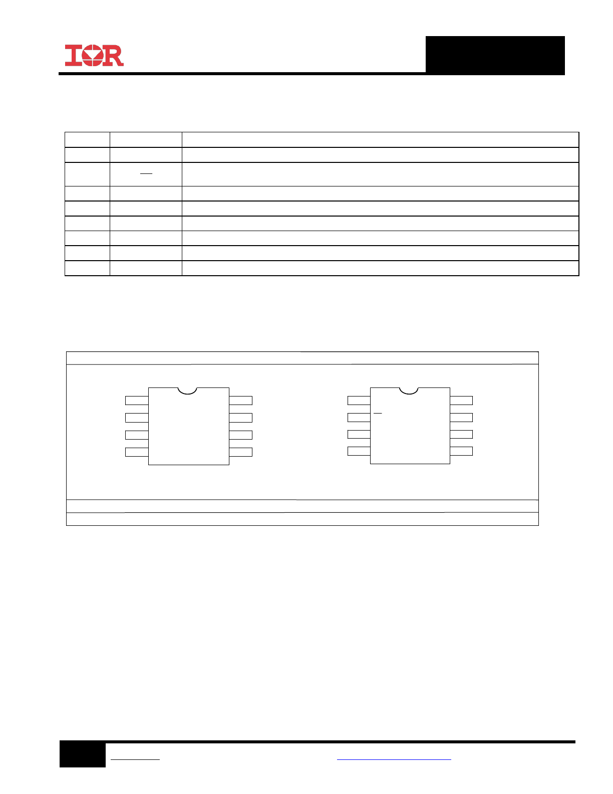
Lead Definitions
PIN
Symbol
Description
1
V
CC
Low-side and logic fixed supply
2
IN
IN
Logic input for gate driver output (HO), in phase with HO (AUIRS2117)
Logic input for gate driver output (HO), out of phase with HO (AUIRS2118)
3
COM
Logic ground
4
NC
No Connection
5
NC
No Connection
6
V
S
High-side floating supply return
7
HO
High-side gate drive output
8
V
B
High-side floating supply
Lead Assignments
AUIRS2117S
8 Lead SOIC
8
7
6
5
V
CC
V
B
IN
1
2
3
4
V
S
HO
COM
Part Number
AUIRS2118S
8 Lead SOIC
8
7
6
5
V
CC
V
B
IN
1
2
3
4
V
S
HO
COM
AUIRS211(7,8)S
9
www.irf.com
© 2014 International Rectifier
Submit Datasheet Feedback
July 15, 2014
Application Information and Additional Details
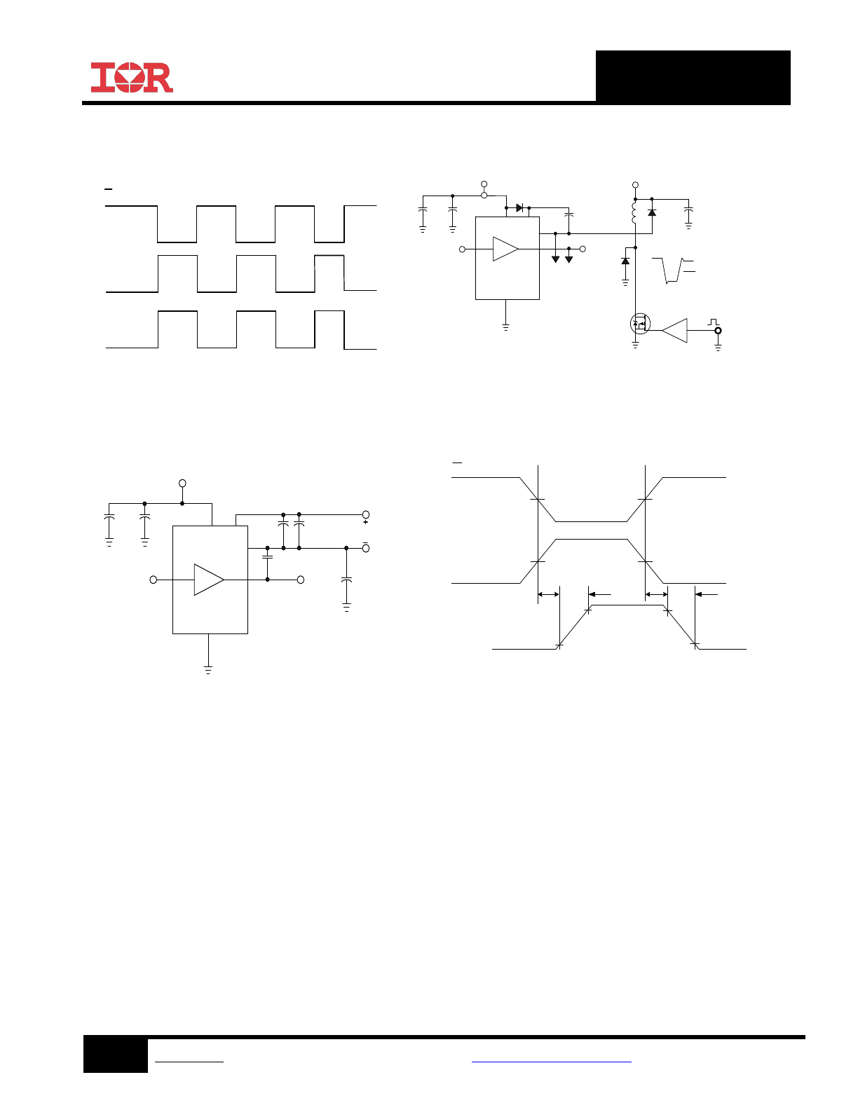
Figure 1: Input/Output Timing Diagram
Figure 2: Floating Supply Voltage Transient
Test Circuit
Figure 3: Switching Time Test Circuit
2
1
3
6
8
7
10 µF
0.1
µF
V
CC
= 15 V
0.1
µF
HO
10
µF
10 µF
V
B
V
S
(O V to 600 V)
15 V
C
L
IN
AUIRS2117
AUIRS2118
Figure 4: Switching Time Waveform
Definition
2
AUIRS2117
3
1
6
8
7
10 µF
0.1
µF
V
CC
= 15 V
10 k F6
0.1
µF
OUTPUT
MONITOR
HO
HV = 10 V to 600 V
10 k F6
10 k
F6
200
µH
100 µF
dV
s
dt
AUIRF820
> 50 V/ns
+
AUIRS2118
IN
(AUIRS2117)
HO
IN
(AUIRS2118)
t
r
IN
t
f
t
on
HO
t
off
(AUIRS2118)
IN
(AUIRS2117)
90%
90%
10%
10%
50%
50%
50%
50%
AUIRS211(7,8)S
10
www.irf.com
© 2014 International Rectifier
Submit Datasheet Feedback
July 15, 2014
Tolerant to Negative V
S
Transients
A common problem in today’s high-power switching converters is the transient response of the switch node’s
voltage as the power switches transition on and off quickly while carrying a large current. A typical half bridge
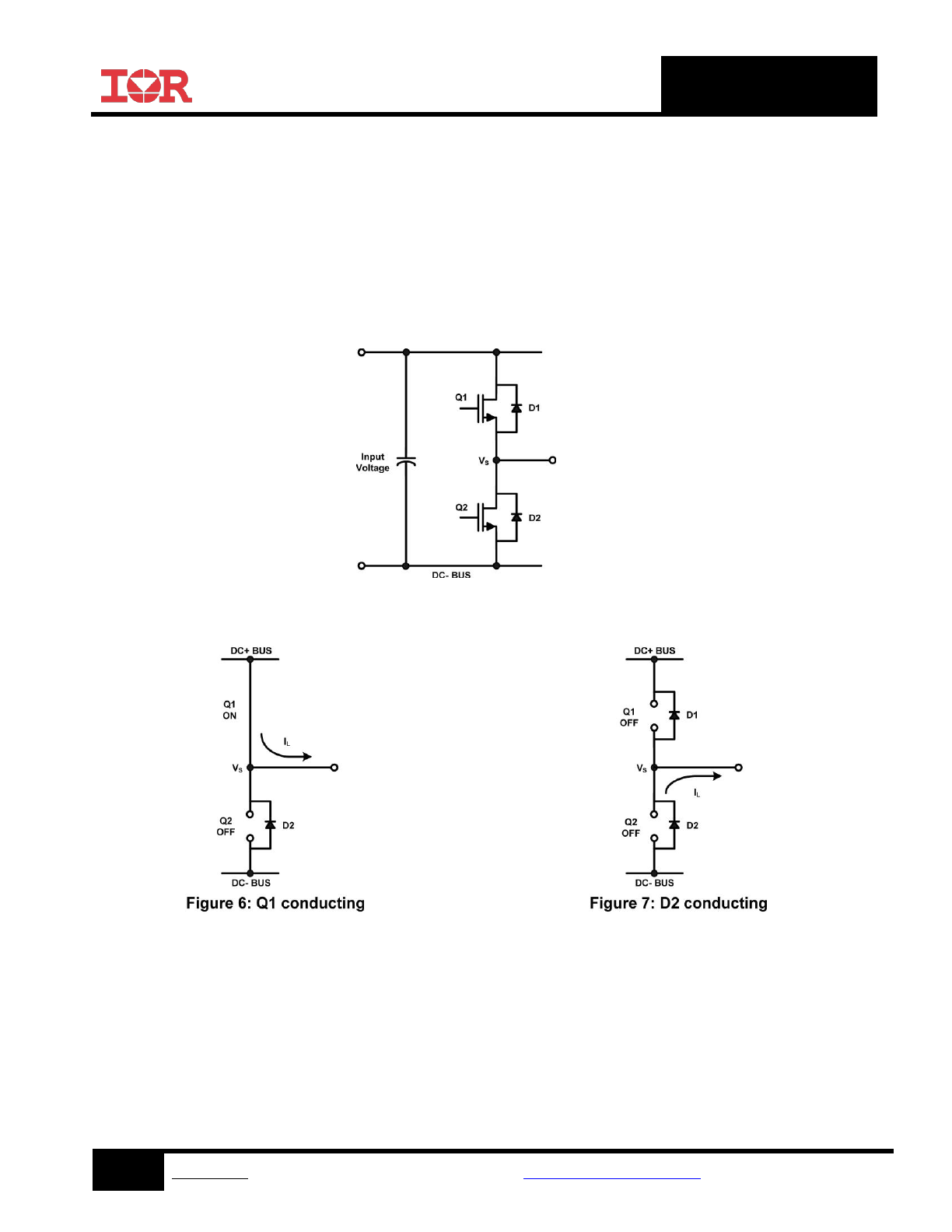
circuit is shown in Figure 5; here we define the power switches and diodes of the inverter.
If the high-side switch (e.g., Q1 in Figures 6 and 7) switches off, while the current is flowing to a load, a current
commutation occurs from high-side switch (Q1) to the diode (D2) in parallel with the low-side switch of the
inverter. At the same instance, the voltage node VS swings from the positive DC bus voltage to the negative
DC bus voltage.
Figure 5: Half Bridge Circuit
Also when the current flows from the load back to the inverter (see Figures 8 and 9), and Q2 switches on, the
current commutation occurs from D1 to Q2. At the same instance, the voltage node V
S
swings from the positive
DC bus voltage to the negative DC bus voltage.