
1
www.irf.com
© 2014 International Rectifier
Submit Datasheet Feedback
May 28, 2014
May 2
nd
, 2014
Automotive Grade
AUIRS20302S
Pre-regulated Three Phase Gate Driver
Features
• 3 phase gate driver for 24V & higher drives
• Under-voltage lockout for all channels
• Cross-conduction prevention logic
• High voltage pre-regulator MOSFET
• Power-on reset architecture
• FAULT detection and Reset
• Current sense comparator
• Over-current blanking time
• 3.3V logic compatible
• Matched propagation delay for all channels
• Fully operational up to +200V
• Floating channels for bootstrap operation
• High negative transients immunity
• Pre-regulated supply line for uP
• Automotive qualified
• Leadfree, RoSH Compliant
Typical Applications
24V to 150V – 3 Phase Motor Drives
Automotive & Truck HVAC, PUMP
BLDC Motor Drives
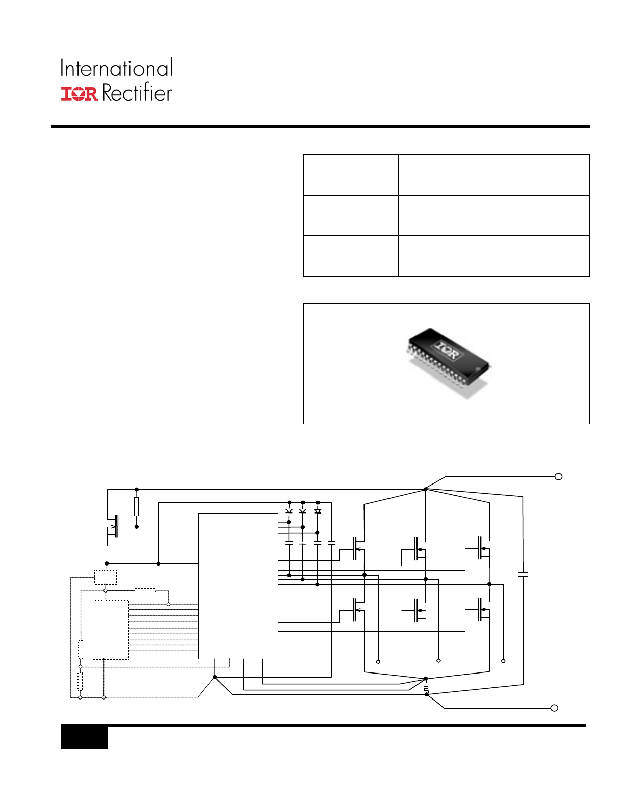
Typical Connection Diagram
Product Summary
Topology
3-phase gate driver
V
OFFSET
200 V
V
OUT
8.0 V – 17 V
I
o+
& I
o-
(typical)
0.20 A & 0.35 A
t
ON
& t
OFF
(typical)
530 ns / 530 ns
Deadtime
(typical)
0.7 us
Package
SOIC 28WB
+ Bat
- Bat
U
V
W
AUIRS20302S
VPR
VCP
Vb1
Lin1
Vb2
Vs1
Vs2
Vs3
Ho1
Ho2
Ho3
Lo1
Lo2
Lo3
Cap
Com
Can
Vss
Ref
5V Reg
ASIC
or uP
Lin2
Lin3
Hin1
Hin2
Hin3
Flt
Frst
EN
Vb3
AUIRS20302S
2
www.irf.com
© 2014 International Rectifier
Submit Datasheet Feedback
May 28, 2014
Table of Contents
Page
Typical Connection Diagram
1
Description/Feature Comparison
3
Qualification Information
4
Absolute Maximum Ratings
5
Recommended Operating Conditions
5
Static Electrical Characteristics
6
Dynamic Electrical Characteristics
7
Functional Block Diagram
8
Input/Output Pin Equivalent Circuit Diagram
9
Lead Definitions
10
Lead Assignments
10
Application Information and Additional Details
11
Parameter Temperature Trends
16
Package Details
21
Tape and Reel Details
22
Part Marking Information & Ordering Information
23

AUIRS20302S
3
www.irf.com
© 2014 International Rectifier
Submit Datasheet Feedback
May 28, 2014
Description
The AUIRS20302S is a three phase gate driver dedicated to BLDC motor drive up to 600W. Proprietary HVIC
technology enables this rugged monolithic design with enforced Automotive ESD & Latch-up grades. Primarily
designed for 24V battery application, its drive capability goes from 12v to 200V which cover all the abnormal
conditions of the vehicle. The gate drive circuitry features cross-conduction preventive and minimum dead-time
blocks. It is powered by a constant voltage so that the gate drives never exceed 17V including during Load Dump
condition.
An external MOSFET is acting as a pre-regulator. The inner charge pump and voltage control loop drives its gate in
order to keep the VPR pin constant when the battery voltage varies. The AUIRS20302S also features an over-
current protection that definitively shuts down all gates in case of short-circuit. The fault condition is reset by cycling
the FRST pin while the I.C is disabled. A blanking time, synchronized with each high side switch command, avoids
any premature triggering of the protection.
The logic control block of the AUIRS20302S is developed in order to support a fast and reliable 3 phase BLDC
design. For example, its inputs are compatible with the 3.3V logic processors and feature a short-pulse/noise
rejection filter. The 6 commands include matched propagation delays, shoot-through protections and minimum
dead-time. The bootstrap capacitor voltage of each phase is monitored independently (UVLO). Also, the maximum
gate voltage is controlled by the pre-regulator in all conditions. No linear or abnormal gate drive is possible. The
VPR pin can also supply the surrounding system components if the total consumption doesn’t exceed 0.1A.
AUIRS20302S
4
www.irf.com
© 2014 International Rectifier
Submit Datasheet Feedback
May 28, 2014
Qualification Information
†
Qualification Level
Automotive
(per AEC-Q100
††
)
Comments: This family of ICs has passed an Automotive
qualification. IR’s Industrial and Consumer qualification level is
granted by extension of the higher Automotive level.
Moisture Sensitivity Level
SOIC28
MSL3
†††
260°C
(per IPC/JEDEC J-STD-020)
ESD
Machine Model
M1 (+/-200V)
(per AEC-Q100-003)
Human Body Model
H1B (+/-2000V)
(per AEC-Q100-002)
Charged Device Model
C3B (+/-500 V)
(per AEC-Q100-011)
IC Latch-Up Test
Class II Level A
(per AEC-Q100-004)
RoHS Compliant
Yes
†
Qualification standards can be found at International Rectifier’s web site
http://www.irf.com/
††
Exceptions to AEC-Q100 requirements are noted in the qualification report.
†††
Higher MSL ratings may be available for the specific package types listed here. Please contact your International
Rectifier sales representative for further information.

AUIRS20302S
5
www.irf.com
© 2014 International Rectifier
Submit Datasheet Feedback
May 28, 2014
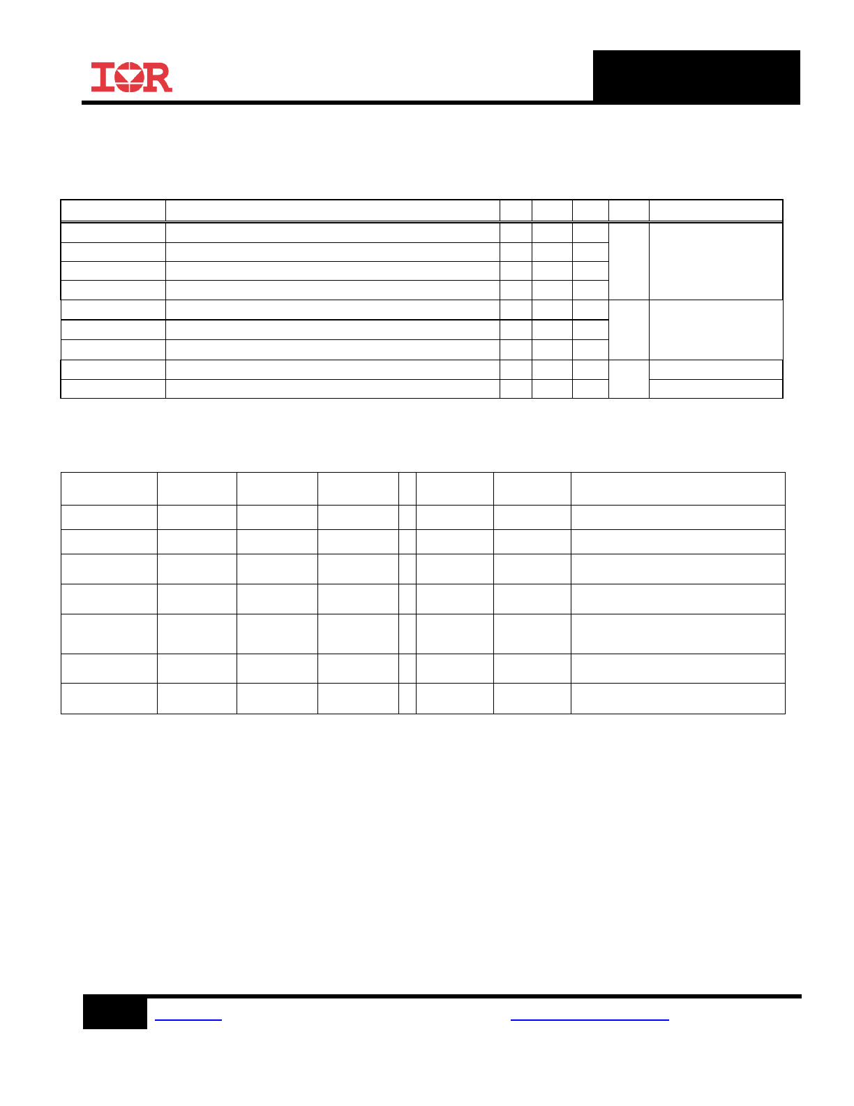
Absolute Maximum Ratings
Absolute Maximum Ratings indicate sustained limits beyond which damage to the device may occur. All voltage parameters are absolute
voltages referenced to VSS, all currents are defined positive into any lead. An operation above the absolute maximum limit is not implied and
could damage the part. The thermal resistance and power dissipation ratings are measured under board mounted and free air conditions
Symbol
Definition
Min.
Max.
Units
V
B1,2,3
High side floating supply voltage
-0.3
220
V
V
HO1,2,3
High side floating output voltage
V
S1,2,3
- 0.3 V
B 1,2,3
+ 0.3
V
S1,2,3
High side offset voltage
V
B 1,2,3
- 20
V
B 1,2,3
+ 0.3
VPR
Low side supply voltage
-0.3
17
VCP
Charge pump output voltage
-0.3
17
COM
Power ground
-5
5
V
LO1,2,3, / FLT
Low side output voltage LO#; FLT pin
-0.3
VPR + 0.3
V
IN
Input pin voltage
(LIN#, HIN#,)
-0.3
VPR + 0.3
Can/Cap
Over-current comparator inputs
-0.3
VPR + 0.3
EN/Frst
Enable & Fault Reset inputs
-0.3
VPR + 0.3
dV/dt
High side floating voltage slew rate
—
50
V/ns
Rth
JA
Junction to ambient thermal resistance
—
80
°C/W
T
J
Maximum operating junction temperature
150
°C
T
S
Maximum storage temperature
-55
150
T
Reflow
Reflow max. temperature (60 sec.)
—
260
Recommended Operating Conditions
The Input/Output timing diagram is shown in figure 1. For proper operation the device should be used within the recommended conditions.
All voltage parameters are referenced to VSS. The VS & COM offset rating are tested with all supplies biased at 15V differential.
Symbol
Definition
Min.
Max.
Units
V
B1,2,3
High side floating supply voltage
V
S1,2,3
+6
V
S1,2,3
+19
V
V
HO 1,2,3
High side output voltage HO#
V
S1,2,3
-0.3
V
B1,2,3
+0.3
V
S 1,2,3
High side floating supply voltage
(Note 1)
200
VPR
Low side supply voltage
6
17
V
LO1,2,3
Low side output voltage LO#
-0.3
VPR+0.3
COM
Power ground
-5
5
V
HO1,2,3
High side output voltage
V
S1,2,3
V
B1,2,3
V
LO1,2,3
Low side output voltage
COM
VPR
V
IN
Logic input voltage LIN, HIN, EN, CAp, CAn, FRST
V
SS
-0.3
VPR
Vcan/cap
Common mode voltage on the CAN & CAP inputs
0
5
VCP
Charge Pump Output Voltage
-
15
Note 1: Logic operational for V
S
between COM -5V to COM +200V. Logic state held for V
S
of COM -5 to COM – V
BS.
(Please refer to the Design Tip DT97 -3 for more details).
AUIRS20302S
6
www.irf.com
© 2014 International Rectifier
Submit Datasheet Feedback
May 28, 2014
Static
Electrical Characteristics
Unless otherwise noted, these specifications apply for an operating junction temperature range of -40
°C ≤ Tj ≤ 125°C with bias conditions of
VBIAS (VPR,VBS 1,2,3) = 15V. The VIN , VTH and IN parameters are referenced to VSS and are applicable to all six channels (HS 1,2,3
and LS 1,2,3). The VO and IO parameters are referenced to COM and VS 1,2,3 and are applicable to the respective output leads: LO1,2,3
and HO1,2,3.
Symbol
Definition
Min Typ Max Units Test Conditions
VIN,th+
Input positive going threshold
(Hin#, Lin#, EN, FRST)
-
1.9
2.5
V
VIN,th-
Input negative going threshold
(Hin#, Lin#, EN, FRST)
0,7
1
-
Iin+
Input bias current
(Lin#, Hin#, EN, FRST)
15
100
220
µA
Vin=5V
Iin-
Input bias current
(Lin#, Hin#, EN, FRST)
-1
0
1
Vin=0V
VPR,UVth+
VPR supply undervoltage positive going threshold
(note 2)
6.4
7.2
8,2
V
VPR,UVth-
VPR supply undervoltage negative going threshold
(note 2)
6
6.7
7.6
VPR,UVhys
VPR supply undervoltage hysteresis
(note 2)
0.4
0.5
0.7
VBS, UVth+
VBS supply undervoltage positive going threshold
6.4
7.2
8,2
VBS, UVth-
VBS supply undervoltage negative going threshold
6
6.7
7.6
VBS, UVhys
VBS supply undervoltage hysteresis
0.4
0.5
0.7
I
LK
Offset supply leakage current
-
5
50
µA
VB=VS=200V
Iqbs
Quiescent VBS supply current
20
45
120
Iqpr
Quiescent VPR supply current
1
2,5
5
mA
VPR=14V
V
OH
High level output voltage, VPR – VO, HO#
0,2
0.9
1.4
V
Io =20mA
V
OL
Low level output voltage, VO, HO#
0,05
0.2
0.6
Io+
Output high short circuit pulsed current, HO#,LO#
105
200
450
mA
Vo =0V,
PW ≤10 µs
Io-
Output low short circuit pulsed current, HO#,LO#
210
350
650
mA
Vo =15V,
PW ≤10 µs
VCP
Charge pump output voltage
VPR=4V
5
6
7,5
V
R
ext
=100kΩ
VPR=8V
10
13
15
VPR=9V
13
15
17
VPR=14V
13
15
17
ICP+
Charge Pump source current
VPR=6V
100
200
400
µA
VPR=14V
200
500 1000
ICP-
Charge Pump sink current
-
5
10
mA
Vcl_Vcp
Vcp pin Active Clamp
17
18.6
21
Icp=10mA
V
FLT
FLT low output voltage
-
-
0.8
V
I
FLT
= 10mA
Ican
1
Comparator input high bias current
-
-
7
µA
Can=5V
Ican
0
Comparator input low bias current
-
-
7
Can=0V
Voff
Comparator input offset
-33
-
33
mV
Vcap= 5V
Tfrst
Minimum FAULT RESET time
20
-
-
us
Ton_EN
Minimum ENABLE time
20
-
-
us
(note 2):. UVPR is latched; when VPR>UVPR, FAULT remains pulled down. This leads to have the FAULT active and latched at VPR ramp
up if no fault reset occurs.
AUIRS20302S
7
www.irf.com
© 2014 International Rectifier
Submit Datasheet Feedback
May 28, 2014
Dynamic Electrical Characteristics
Unless otherwise noted, these specifications apply for an operating junction temperature range of -40
°C ≤ Tj ≤ 125°C with bias conditions of
VPR = VBS = 15V, VS1,2,3 = VSS = COM, and CL = 1000 pF.
Symbol
Definition
Min Typ Max Units
Test Conditions
Ton
Turn-on propagation delay, LO#, HO#
350 550
850
nS
V
IN
= 0 & 5V
Toff
Turn-off propagation delay, LO#, HO#
350 600
850
LOt
r
, HOt
r
Turn-on rise time LO#, HO#
10
100
300
LOt
f
, HOt
r
Turn-off fall time LO#, HO#
5
35
75
T
OC
Over-current to output shutdown response time
-
1
1.7
uS
V
(Can)
-V
(Cap)
=1V
T
FLT
Over-current FLT response time
-
0.7
1.2
t
blank
Current limit blanking time
5
6
7.5
tFILIN
Input filter time (HIN, LIN)
200 270
510
nS
V
IN
= 0 & 5V
DT
Dead-time
420 700 1000
VPR=15V
Truth Table
This table is valid for voltages ranges defined in the recommended operating conditions section.
ENABLE
CAN>CA
P
FRST
LIN#/HIN
#
LO#/HO#
FLT
Comments
0
0
0
X
0
No Change
FLT keeps showing same status
0
1
0
X
0
Vss
0
0
1
X
0
Open
FLT Reset Sequence (Note3)
0
1
1
X
0
Vss
1
0
X
LIN#/HIN#
LO#/HO#
Open
Normal Operation: An anti-shoot-through
logic prevents each channel from turning on
simultaneously the HS and LS switches
1
1
0
LIN#/HIN#
0
Vss
Over-current detection (FLT)
1 *
1 *
1 *
LIN#/HIN# *
LO#/HO# *
Open*
* Not recommended
(cycling on default)
Note 3: The proper sequence to reset the Fault latch is to first set EN at 0V and then cycle the FRST pin. The gate drives return to normal
operation when EN is set again at 5V.
AUIRS20302S
8
www.irf.com
© 2014 International Rectifier
Submit Datasheet Feedback
May 28, 2014
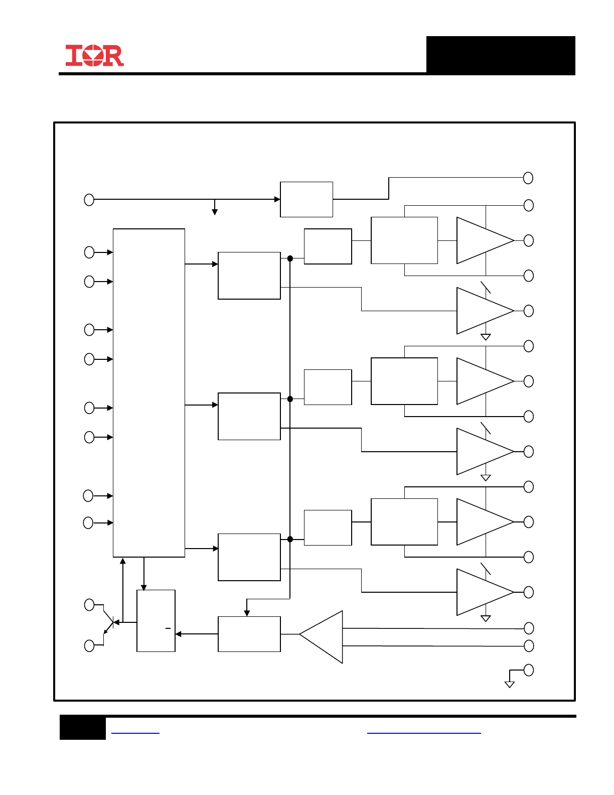
Functional Block Diagram
Lin1
EN
Hin1
Hin2
Hin3
Lin2
Lin3
Deadtime &
shoot-through
protection
HV level
shifter
Latch &
Undervoltage
detection
Driver
VB1
HO1
VS1
Driver
LO1
Deadtime &
shoot-through
protection
HV level
shifter
Latch &
Undervoltage
detection
Driver
VB2
HO2
VS2
Driver
LO2
Deadtime &
shoot-through
protection
HV level
shifter
Latch &
Undervoltage
detection
Driver
VB3
HO3
VS3
Driver
LO3
Over-current
Blanking time
+
_
CAp
CAn
Logic
Control
VPR
Pre-
Regulation
Control
VCP
COM
VSS
Q
R
S
Fault
latch
FRST
FLT
Vcc
AUIRS20302S
9
www.irf.com
© 2014 International Rectifier
Submit Datasheet Feedback
May 28, 2014
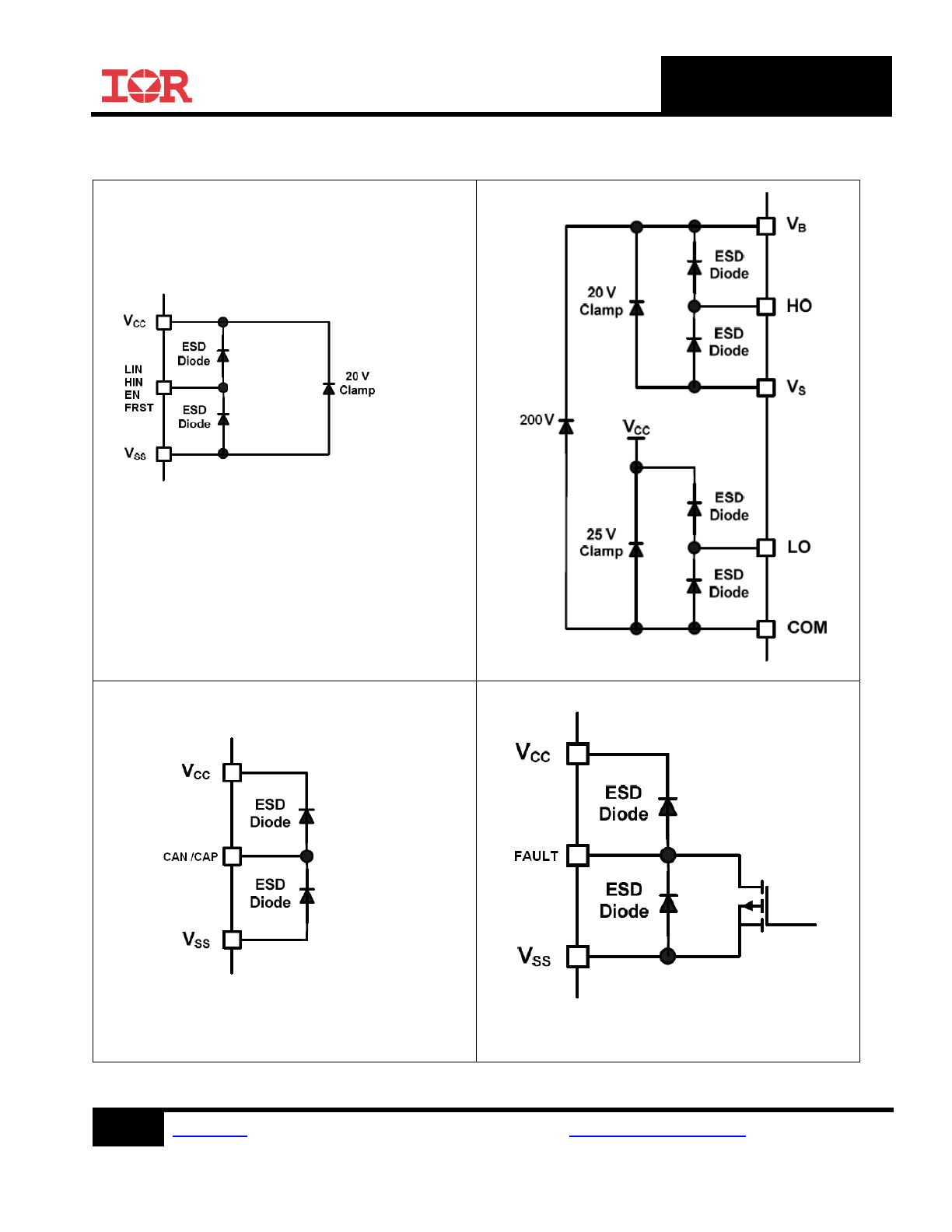
Input/Output Pin Equivalent Circuit Diagram
AUIRS20302S
10
www.irf.com
© 2014 International Rectifier
Submit Datasheet Feedback
May 28, 2014
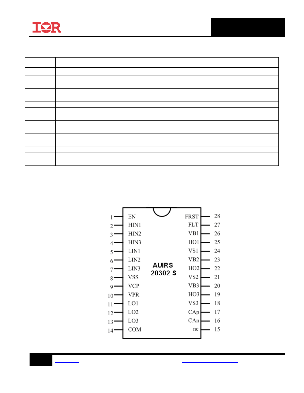
Lead Definitions
Symbol
Description
HIN#
Input for high side gate drive – Active high
LIN#
Input for low side gate drive – active high
VSS
Logic Ground
VCP
Pre-regulated MOSFET gate output – Analog gate drive
VPR
Power supply pin of the I.C (equivalent to Vcc)
LO#
Low side gate driver outputs (1,2 & 3)
COM
Common low side gate drive return pin & Power Ground
CAP
Non inverting input of the over-current comparator
CAN
Inverting input of the over-current comparator
VS#
High side floating supply return (1, 2 & 3)
HO#
High side gate driver outputs (1, 2 & 3)
VB#
High side floating supply (1, 2 & 3)
EN
Enable input – Active high
FAULT
Fault output pin – Open collector
FRST
Fault Reset input pin – Active high
Lead Assignments