
AUIRLR014N
V
DSS
55V
R
DS(on)
max.
0.14
I
D
10A
Features
Advanced Planar Technology
Logic Level Gate Drive
Low
On-Resistance
Dynamic dV/dT Rating
175°C Operating Temperature
Fast Switching
Fully Avalanche Rated
Repetitive Avalanche Allowed up to Tjmax
Lead-Free, RoHS Compliant
Automotive Qualified *
Description
Specifically designed for Automotive applications, this cellular
design of HEXFET® Power MOSFETs utilizes the latest
processing techniques to achieve low on-resistance per silicon
area. This benefit combined with the fast switching speed and
ruggedized device design that HEXFET power MOSFETs are well
known for, provides the designer with an extremely efficient and
reliable device for use in Automotive and a wide variety of other
applications.
1
2015-12-11
HEXFET® is a registered trademark of Infineon.
*Qualification standards can be found at
www.infineon.com
AUTOMOTIVE GRADE
Symbol Parameter
Max.
Units
I
D
@ T
C
= 25°C
Continuous Drain Current, V
GS
@ 10V
10
A
I
D
@ T
C
= 100°C
Continuous Drain Current, V
GS
@ 10V
7.1
I
DM
Pulsed Drain Current 40
P
D
@T
C
= 25°C
Maximum Power Dissipation
28
W
Linear Derating Factor
0.2
W/°C
V
GS
Gate-to-Source Voltage
± 16
V
E
AS
Single Pulse Avalanche Energy (Thermally Limited) 35
mJ
I
AR
Avalanche Current 6.0
A
E
AR
Repetitive Avalanche Energy 2.8
mJ
T
J
Operating Junction and
-55 to + 175
T
STG
Storage Temperature Range
°C
Soldering Temperature, for 10 seconds (1.6mm from case)
300
dv/dt
Peak Diode Recovery 5.0
V/ns
Absolute Maximum Ratings
Stresses beyond those listed under “Absolute Maximum Ratings” may cause permanent damage to the device. These are stress
ratings only; and functional operation of the device at these or any other condition beyond those indicated in the specifications is not
implied. Exposure to absolute-maximum-rated conditions for extended periods may affect device reliability. The thermal resistance
and power dissipation ratings are measured under board mounted and still air conditions. Ambient temperature (TA) is 25°C, unless
otherwise specified.
Thermal Resistance
Symbol Parameter
Typ.
Max.
Units
R
JC
Junction-to-Case –––
5.3
°C/W
R
JA
Junction-to-Ambient ( PCB Mount) –––
50
R
JA
Junction-to-Ambient
–––
110
D-Pak
AUIRLR014N
Base part number
Package Type
Standard Pack
Orderable Part Number
Form
Quantity
AUIRLR014N
D-Pak
Tube
75
AUIRLR014N
Tape and Reel Left
3000
AUIRLR014NTRL
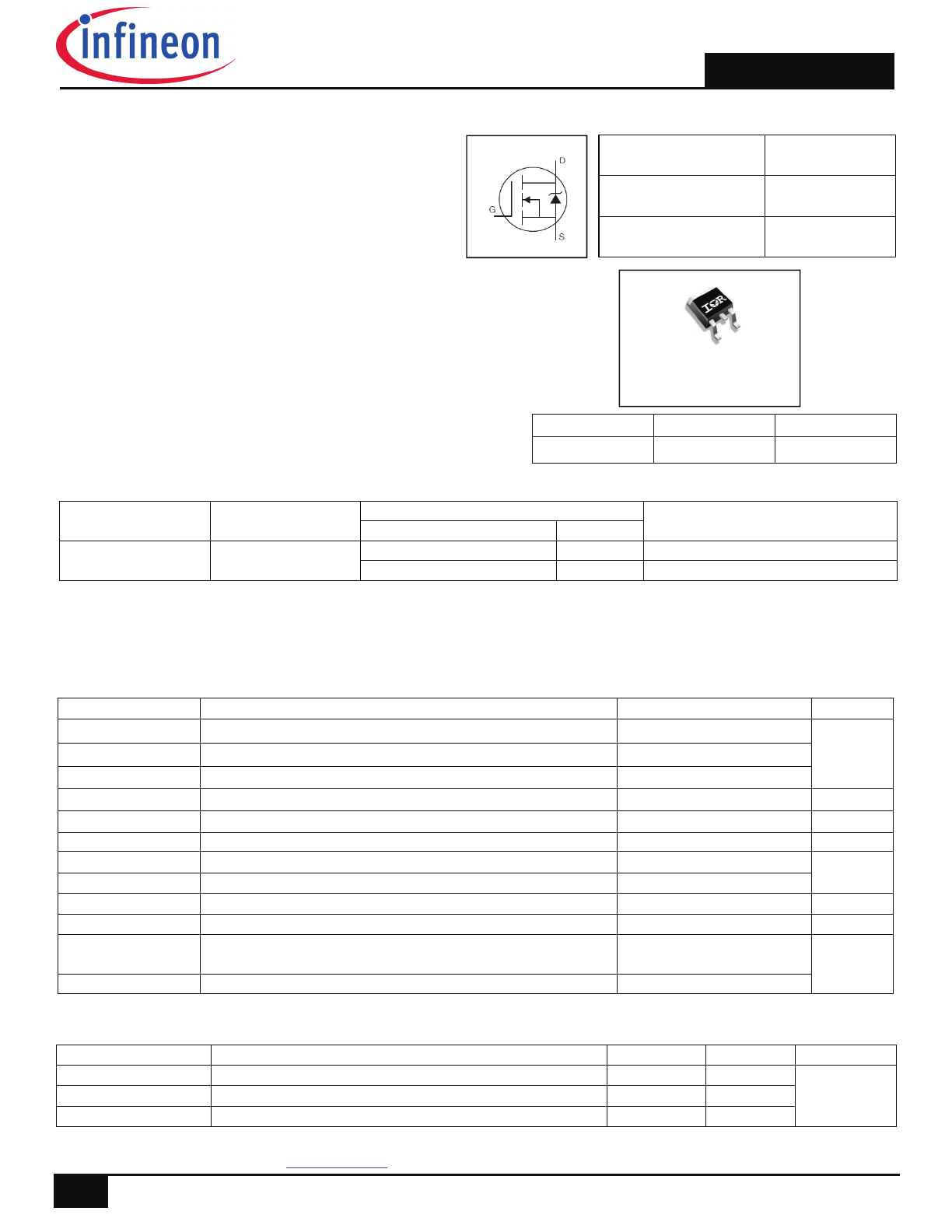
G D S
Gate Drain Source
S
G
D
HEXFET
®
Power MOSFET
AUIRLR014N
2
2015-12-11
Notes:
Repetitive rating; pulse width limited by max. junction temperature. (See fig. 11)
Starting T
J
= 25°C, L = 1.96
m
H, R
G
= 25
, I
AS
= 6A (See fig. 12)
I
SD
6.0A, di/dt 210A/µs, V
DD
V
(BR)DSS
, T
J
175°C.
Pulse width
300
µ
s; duty cycle
2%.
This is applied for I-PAK, L
S
of D-PAK is measured between lead and center of die contact.
When mounted on 1" square PCB (FR-4 or G-10 Material). For recommended footprint and soldering techniques refer to
application note #AN-994
Static @ T
J
= 25°C (unless otherwise specified)
Parameter Min.
Typ.
Max.
Units
Conditions
V
(BR)DSS
Drain-to-Source Breakdown Voltage
55
––– –––
V V
GS
= 0V, I
D
= 250µA
V
(BR)DSS
/
T
J
Breakdown Voltage Temp. Coefficient
––– 0.056 ––– V/°C Reference to 25°C, I
D
= 1mA
R
DS(on)
Static Drain-to-Source On-Resistance
––– ––– 0.14
V
GS
= 10V, I
D
= 6.0A
––– ––– 0.21
V
GS
= 4.5V, I
D
= 5.0A
V
GS(th)
Gate Threshold Voltage
1.0
–––
3.0
V V
DS
= V
GS
, I
D
= 250µA
gfs
Forward Trans conductance
3.1
––– –––
S V
DS
= 25V, I
D
= 6.0A
I
DSS
Drain-to-Source Leakage Current
––– ––– 25
µA
V
DS
= 55V, V
GS
= 0V
––– ––– 250
V
DS
= 55V,V
GS
= 0V,T
J
=150°C
I
GSS
Gate-to-Source Forward Leakage
–––
––– 100
nA
V
GS
= 16V
Gate-to-Source Reverse Leakage
–––
––– -100
V
GS
= - 16V
Dynamic Electrical Characteristics @ T
J
= 25°C (unless otherwise specified)
Q
g
Total Gate Charge
–––
–––
7.9
nC
I
D
= 6.0A
Q
gs
Gate-to-Source Charge
–––
–––
1.4
V
DS
= 44V
Q
gd
Gate-to-Drain Charge
–––
–––
4.4
V
GS
= 5.0V, See Fig. 6 &13
t
d(on)
Turn-On Delay Time
–––
6.5
–––
ns
V
DD
= 28V
t
r
Rise Time
–––
47
–––
I
D
= 6.0A
t
d(off)
Turn-Off Delay Time
–––
12
–––
R
G
= 6.2
V
GS
= 5.0V
t
f
Fall Time
–––
23
–––
R
D
= 4.5
,See Fig. 10
L
D
Internal Drain Inductance
–––
4.5
–––
nH
Between lead,
6mm (0.25in.)
L
S
Internal Source Inductance
–––
7.5
–––
from package
and center of die contact
C
iss
Input Capacitance
–––
265 –––
pF
V
GS
= 0V
C
oss
Output Capacitance
–––
80
–––
V
DS
= 25V
C
rss
Reverse Transfer Capacitance
–––
38
–––
ƒ = 1.0MHz, See Fig.5
Diode Characteristics
Parameter
Min. Typ. Max. Units
Conditions
I
S
Continuous Source Current
––– ––– 10
A
MOSFET symbol
(Body Diode)
showing the
I
SM
Pulsed Source Current
––– ––– 40
integral reverse
(Body Diode)
p-n junction diode.
V
SD
Diode Forward Voltage
–––
–––
1.3
V T
J
= 25°C,I
S
= 6.0A, V
GS
= 0V
t
rr
Reverse Recovery Time
–––
37
56
ns T
J
= 25°C ,I
F
= 6.0A
Q
rr
Reverse Recovery Charge
–––
48
71
nC di/dt = 100A/µs
t
on
Forward Turn-On Time
Intrinsic turn-on time is negligible (turn-on is dominated by L
S
+L
D
)
AUIRLR014N
3
2015-12-11
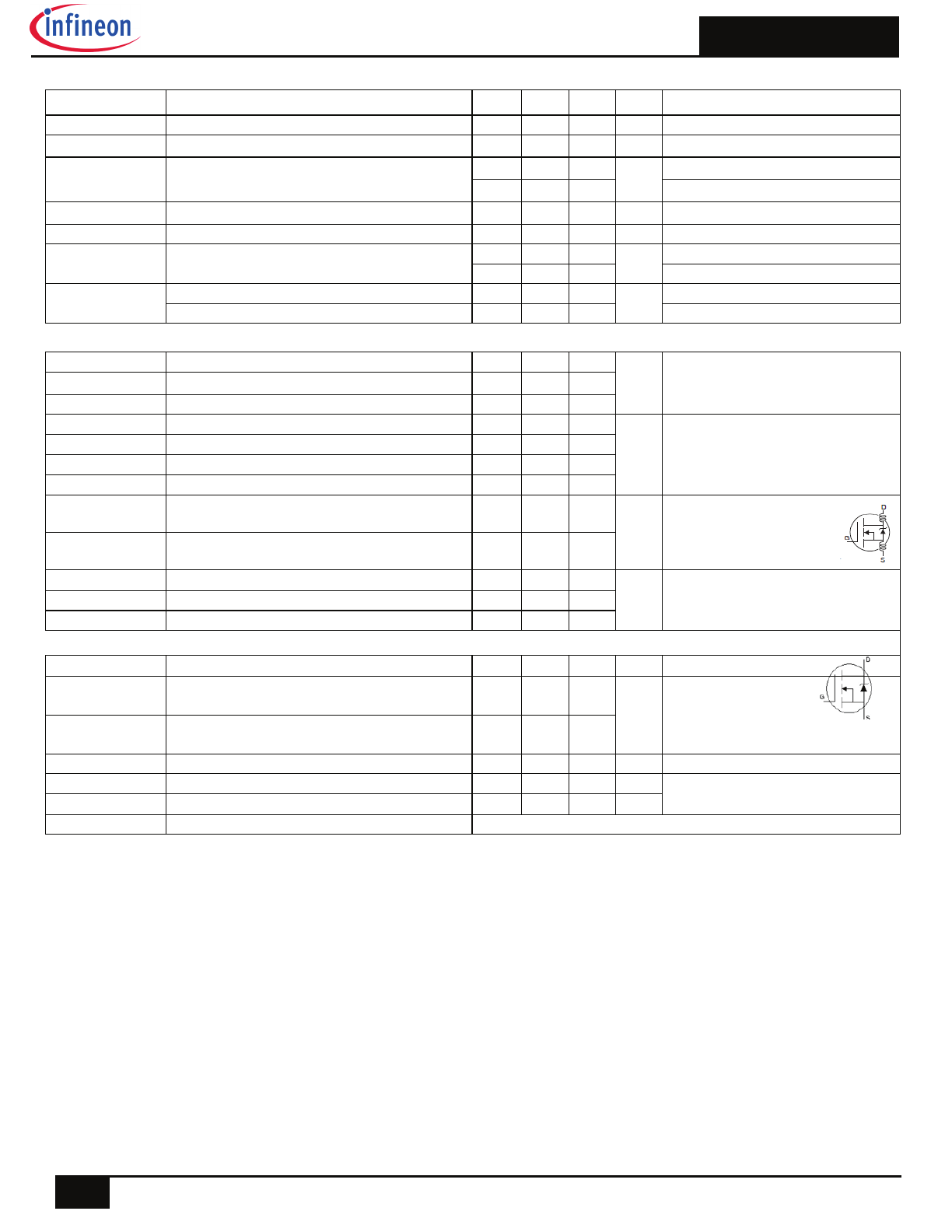
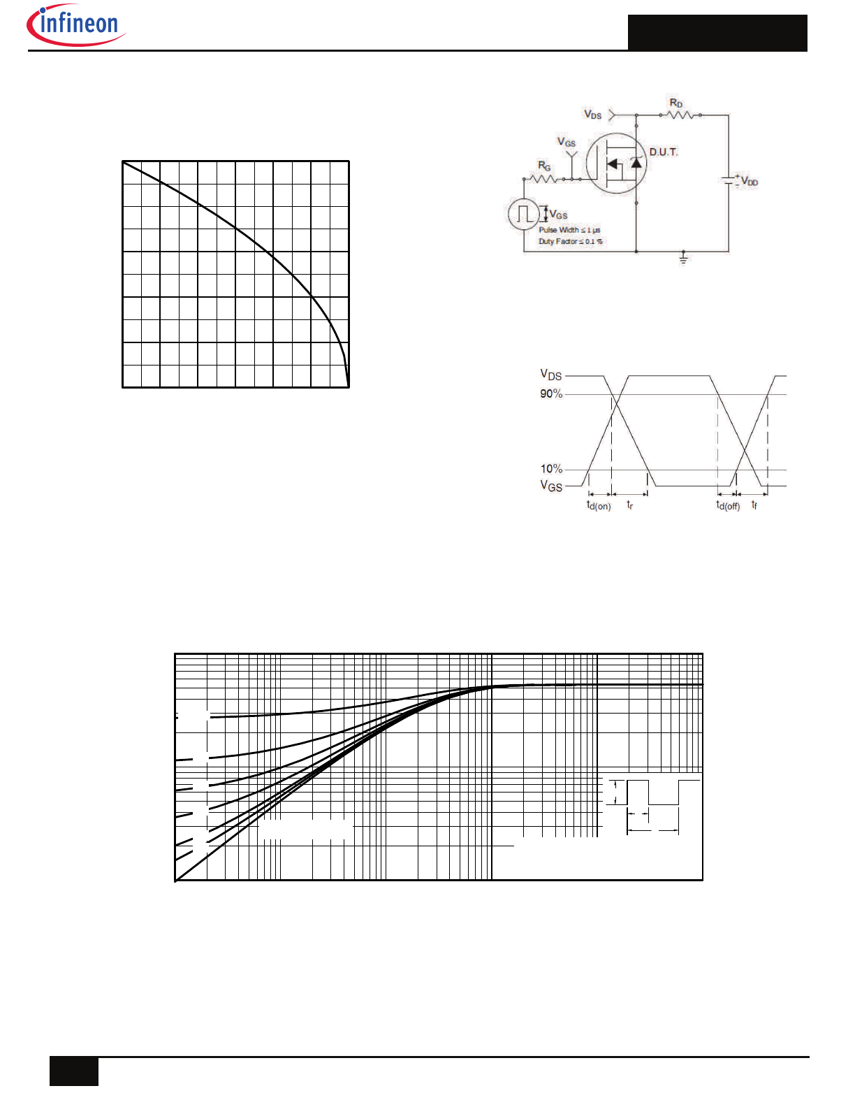
Fig. 2 Typical Output Characteristics
Fig. 3
Typical Transfer Characteristics
Fig. 4 Normalized On-Resistance
Vs. Temperature
Fig. 1 Typical Output Characteristics
0.1
1
10
100
0.1
1
10
100
20µs PULSE WIDTH
T = 25 C
J
°
TOP
BOTTOM
VGS
15V
12V
10V
7.0V
5.0V
4.5V
2.7V
2.0V
V , Drain-to-Source Voltage (V)
I
, D
ra
in
-t
o-S
ou
rc
e
C
urre
nt
(A
)
DS
D
2.5V
V
GS
TOP 15V
10V
5.0V
4.5V
3.5V
3.0V
2.7V
BOTTOM 2.5V
0.1
1
10
100
0.1
1
10
100
20µs PULSE WIDTH
T = 175 C
J
°
TOP
BOTTOM
VGS
15V
12V
10V
7.0V
5.0V
4.5V
2.7V
2.0V
V , Drain-to-Source Voltage (V)
I
, D
rai
n-
to
-S
our
ce
C
ur
ren
t (
A
)
DS
D
2.5V
V
GS
TOP 15V
10V
5.0V
4.5V
3.5V
3.0V
2.7V
BOTTOM 2.5V
0.1
1
10
100
2.0
4.0
6.0
8.0
10.0
V = 50V
20µs PULSE WIDTH
DS
V , Gate-to-Source Voltage (V)
I
,
Dra
in-
to
-S
ou
rc
e Cur
re
nt
(
A
)
GS
D
T = 25 C
J
°
T = 175 C
J
°
-60 -40 -20 0
20 40 60 80 100 120 140 160 180
0.0
0.5
1.0
1.5
2.0
2.5
T , Junction Temperature( C)
R
, Drai
n-
to
-Sour
ce
O
n
Re
si
st
anc
e
(No
rma
liz
ed)
J
D
S(
on)
°
V
=
I =
GS
D
10V
10A
AUIRLR014N
4
2015-12-11
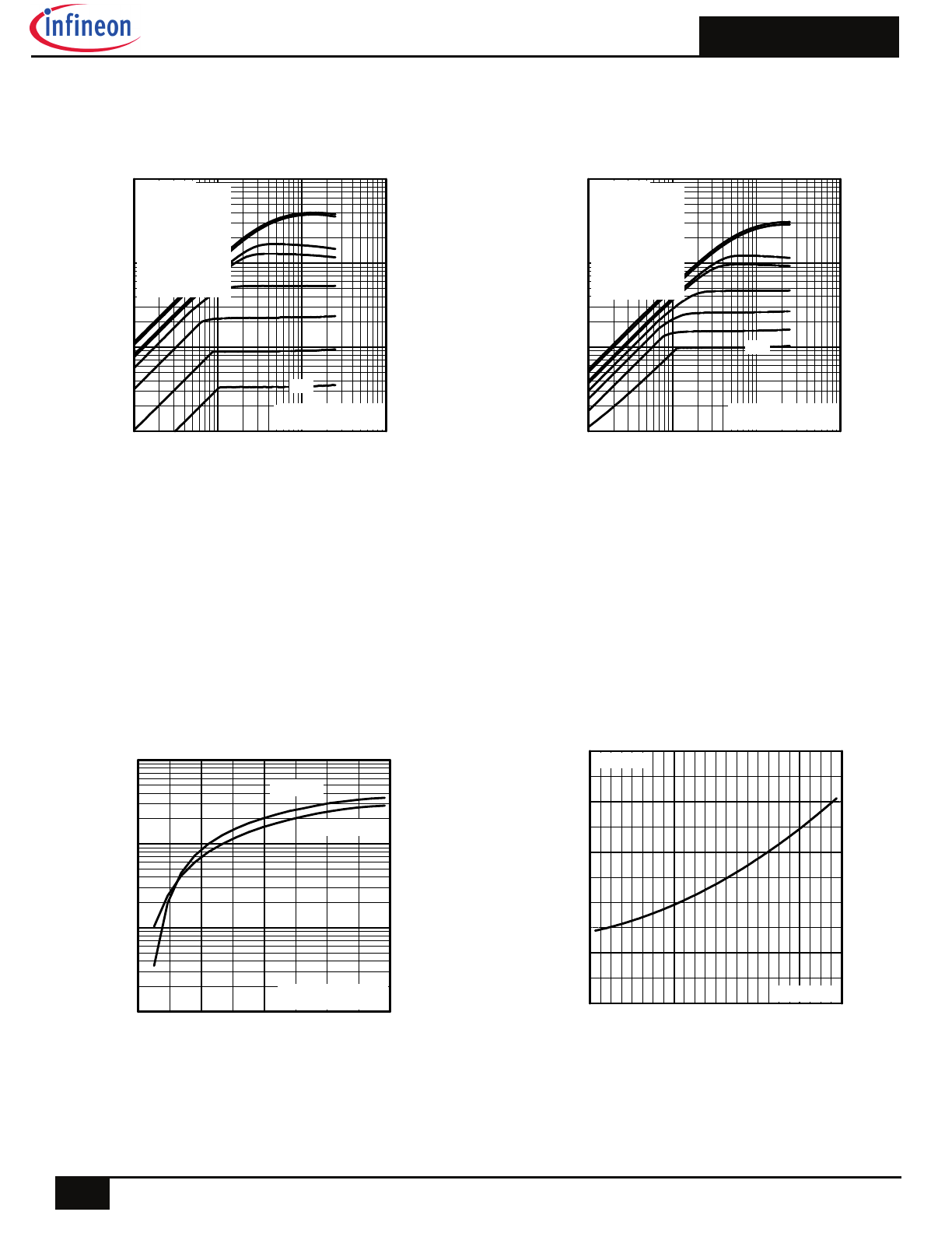
Fig 5. Typical Capacitance vs.
Drain-to-Source Voltage
Fig 6. Typical Gate Charge vs.
Gate-to-Source Voltage
Fig 8. Maximum Safe Operating Area
Fig. 7 Typical Source-to-Drain Diode
Forward Voltage
1
10
100
0
100
200
300
400
500
V , Drain-to-Source Voltage (V)
C, Cap
acit
ance (pF)
DS
V
C
C
C
=
=
=
=
0V,
C
C
C
f = 1MHz
+ C
+ C
C SHORTED
GS
iss
gs
gd ,
ds
rss
gd
oss
ds
gd
Ciss
Coss
Crss
0
2
4
6
8
10
0
5
10
15
Q , Total Gate Charge (nC)
V
,
G
ate
-t
o-
S
ou
rc
e V
olt
ag
e (
V
)
G
GS
FOR TEST CIRCUIT
SEE FIGURE
I =
D
13
6 A
V
= 27V
DS
V
= 44V
DS
0.1
1
10
100
0.2
0.6
1.0
1.4
1.8
V ,Source-to-Drain Voltage (V)
I
, R
ev
erse
D
ra
in
C
urren
t (A)
SD
SD
V = 0 V
GS
T = 25 C
J
°
T = 175 C
J
°
0.1
1
10
100
1000
1
10
100
OPERATION IN THIS AREA LIMITED
BY R
DS(on)
Single Pulse
T
T
= 175 C
= 25 C
°
°
J
C
V , Drain-to-Source Voltage (V)
I
,
Drai
n C
urr
en
t (
A
)
I
,
Drai
n C
urr
en
t (
A
)
DS
D
10us
100us
1ms
10ms
AUIRLR014N
5
2015-12-11
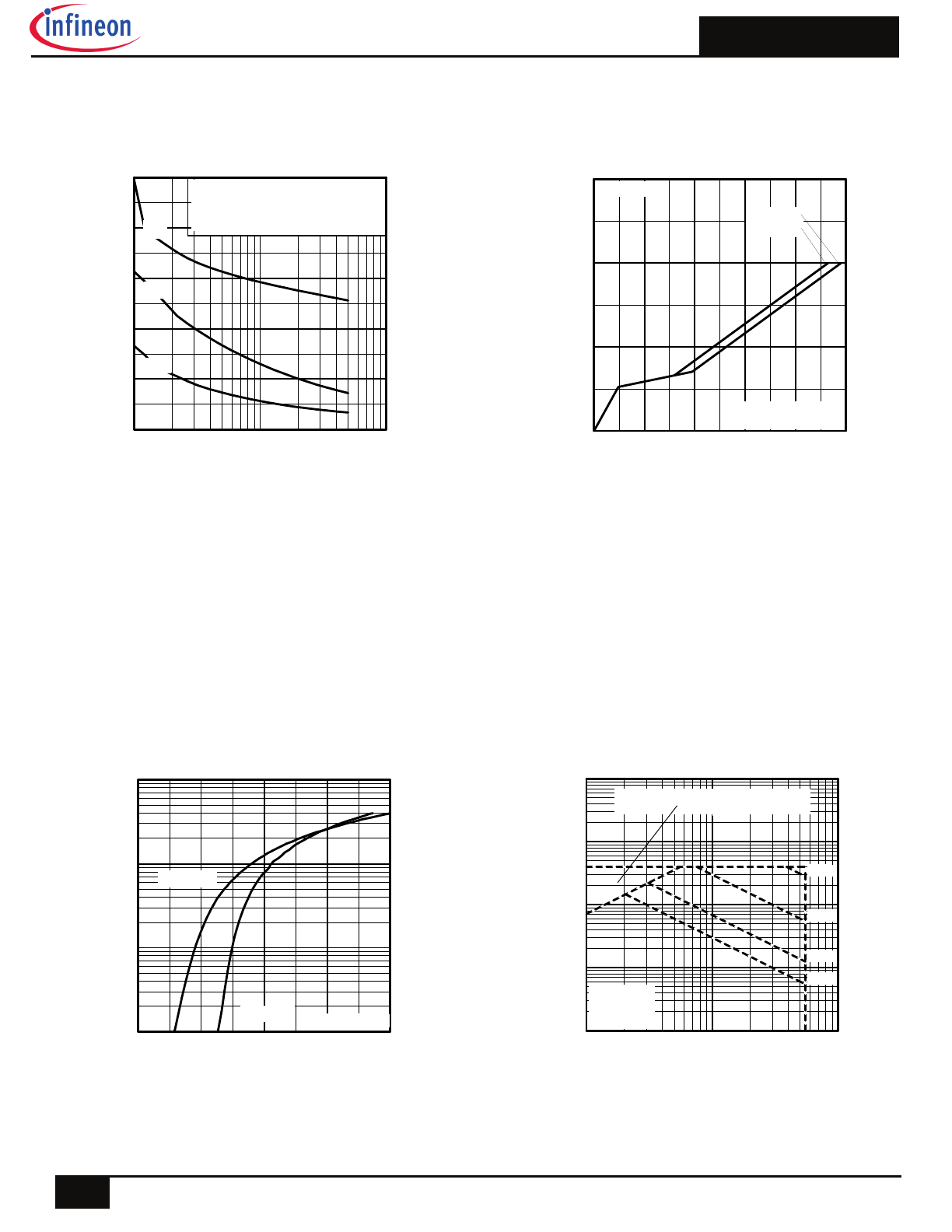
Fig 11. Maximum Effective Transient Thermal Impedance, Junction-to-Case
Fig 9. Maximum Drain Current Vs.
Case Temperature
Fig 10a. Switching Time Test Circuit
Fig 10b. Switching Time Waveforms
25
50
75
100
125
150
175
0.0
2.0
4.0
6.0
8.0
10.0
T , Case Temperature ( C)
I
, D
ra
in C
ur
ren
t (A
)
°
C
D
0.1
1
10
0.00001
0.0001
0.001
0.01
0.1
1
Notes:
1. Duty factor D = t / t
2. Peak T = P
x Z
+ T
1
2
J
DM
thJC
C
P
t
t
DM
1
2
t , Rectangular Pulse Duration (sec)
Ther
m
al
R
espons
e
(Z
)
1
thJ
C
0.01
0.02
0.05
0.10
0.20
D = 0.50
SINGLE PULSE
(THERMAL RESPONSE)
AUIRLR014N
6
2015-12-11
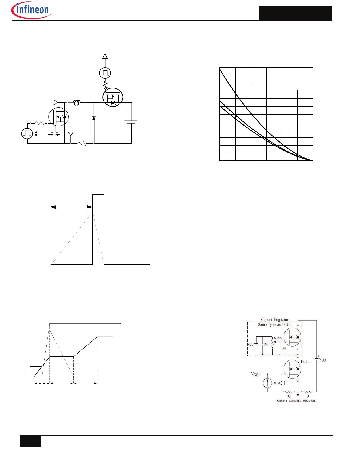
Fig 12c. Maximum Avalanche Energy
vs. Drain Current
Fig 12a. Unclamped Inductive Test Circuit
Fig 12b. Unclamped Inductive Waveforms
RG
IAS
0.01
tp
D.U.T
L
VDS
+
- VDD
DRIVER
A
15V
20V
tp
V
(BR)DSS
I
AS
Fig 13b. Gate Charge Test Circuit
Fig 13a. Gate Charge Waveform
Vds
Vgs
Id
Vgs(th)
Qgs1 Qgs2
Qgd
Qgodr
25
50
75
100
125
150
175
0
10
20
30
40
50
60
Starting T , Junction Temperature ( C)
E
,
S
ing
le
Pu
ls
e
Av
a
la
nc
h
e Ene
rgy
(
m
J)
J
AS
°
ID
TOP
BOTTOM
2.4A
5.0A
6.0A
AUIRLR014N
7
2015-12-11
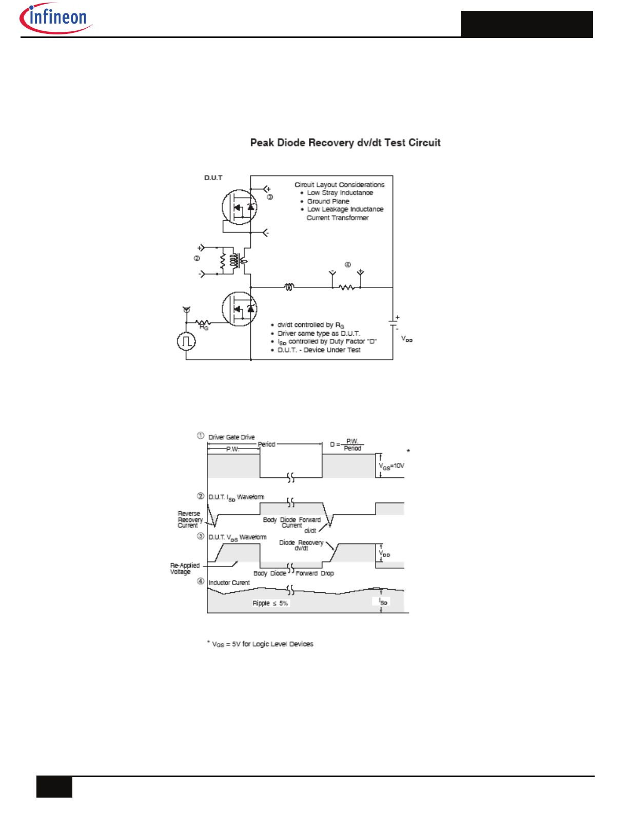
Fig 14. Peak Diode Recovery dv/dt Test Circuit for N-Channel HEXFET® Power MOSFETs
AUIRLR014N
8
2015-12-11
Note: For the most current drawing please refer to IR website at
http://www.irf.com/package/
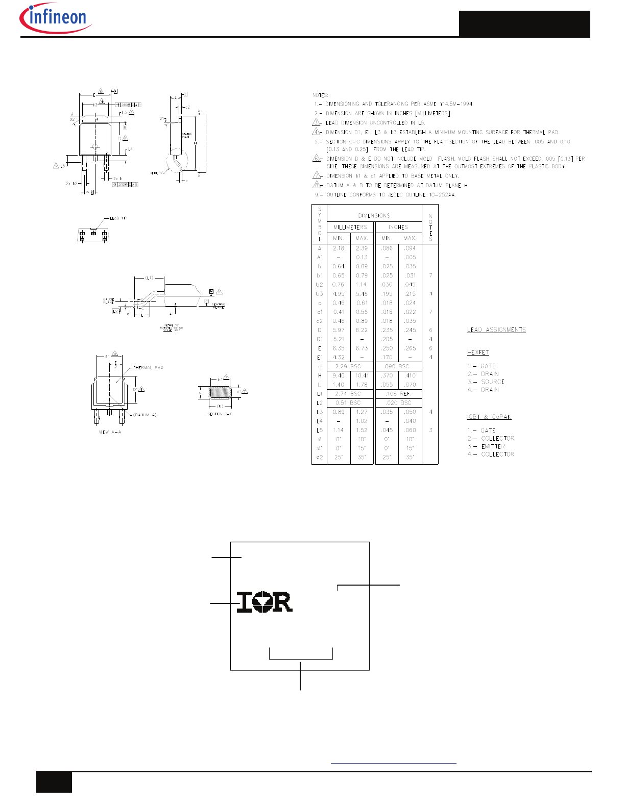
D-Pak (TO-252AA) Package Outline (Dimensions are shown in millimeters (inches))
YWWA
XX
XX
Date Code
Y= Year
WW= Work Week
AULR014N
Lot Code
Part Number
IR Logo
D-Pak (TO-252AA) Part Marking Information
AUIRLR014N
9
2015-12-11
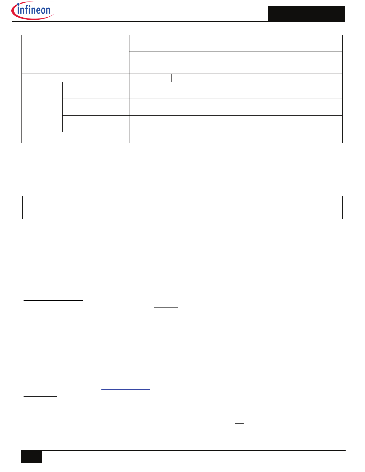
D-Pak (TO-252AA) Tape & Reel Information (Dimensions are shown in millimeters (inches))
Note: For the most current drawing please refer to IR website at
http://www.irf.com/package/
TR
16.3 ( .641 )
15.7 ( .619 )
8.1 ( .318 )
7.9 ( .312 )
12.1 ( .476 )
11.9 ( .469 )
FEED DIRECTION
FEED DIRECTION
16.3 ( .641 )
15.7 ( .619 )
TRR
TRL
NOTES :
1. CONTROLLING DIMENSION : MILLIMETER.
2. ALL DIMENSIONS ARE SHOWN IN MILLIMETERS ( INCHES ).
3. OUTLINE CONFORMS TO EIA-481 & EIA-541.
NOTES :
1. OUTLINE CONFORMS TO EIA-481.
16 mm
13 INCH
AUIRLR014N
10
2015-12-11
Qualification Information
Qualification Level
Automotive
(per AEC-Q101)
Comments: This part number(s) passed Automotive qualification. Infineon’s
Industrial and Consumer qualification level is granted by extension of the higher
Automotive level.
Moisture Sensitivity Level
D-Pak
MSL1
ESD
Machine Model
Class M1B (+/- 75V)
†
AEC-Q101-002
Human Body Model
Class H1A (+/- 300V)
†
AEC-Q101-001
Charged Device Model
Class C5 (+/- 2000V)
†
AEC-Q101-005
RoHS Compliant
Yes
Published by
Infineon Technologies AG
81726 München, Germany
©
Infineon Technologies AG 2015
All Rights Reserved.
IMPORTANT NOTICE
The information given in this document shall in no event be regarded as a guarantee of conditions or characteristics
(“Beschaffenheitsgarantie”). With respect to any examples, hints or any typical values stated herein and/or any
information regarding the application of the product, Infineon Technologies hereby disclaims any and all warranties and
liabilities of any kind, including without limitation warranties of non-infringement of intellectual property rights of any third
party.
In addition, any information given in this document is subject to customer’s compliance with its obligations stated in this
document and any applicable legal requirements, norms and standards concerning customer’s products and any use of
the product of Infineon Technologies in customer’s applications.
The data contained in this document is exclusively intended for technically trained staff. It is the responsibility of
customer’s technical departments to evaluate the suitability of the product for the intended application and the
completeness of the product information given in this document with respect to such application.
For further information on the product, technology, delivery terms and conditions and prices please contact your nearest
Infineon Technologies office (
www.infineon.com
).
WARNINGS
Due to technical requirements products may contain dangerous substances. For information on the types in question
please contact your nearest Infineon Technologies office.
Except as otherwise explicitly approved by Infineon Technologies in a written document signed by authorized
representatives of Infineon Technologies, Infineon Technologies’ products may not be used in any applications where a
failure of the product or any consequences of the use thereof can reasonably be expected to result in personal injury.
Revision History
Date Comments
12/11/2015
Updated datasheet with corporate template
Corrected ordering table on page 1.
† Highest passing voltage.