
AUIRL1404S
AUIRL1404L
V
DSS
40V
R
DS(on)
max.
4.0m
I
D
160A
Absolute Maximum Ratings
Stresses beyond those listed under “Absolute Maximum Ratings” may cause permanent damage to the device. These are stress
ratings only; and functional operation of the device at these or any other condition beyond those indicated in the specifications is not
implied. Exposure to absolute-maximum-rated conditions for extended periods may affect device reliability. The thermal resistance
and power dissipation ratings are measured under board mounted and still air conditions. Ambient temperature (TA) is 25°C, unless
otherwise specified.
Features
Advanced Planar Technology
Logic Level Gate Drive
Low
On-Resistance
Dynamic dV/dT Rating
175°C Operating Temperature
Fast
Switching
Fully Avalanche Rated
Repetitive Avalanche Allowed up to Tjmax
Lead-Free, RoHS Compliant
Automotive Qualified *
Description
Specifically designed for Automotive applications, this Stripe Planar
design of HEXFET® Power MOSFETs utilizes the latest processing
techniques to achieve low on-resistance per silicon area. This
benefit combined with the fast switching speed and ruggedized
device design that HEXFET power MOSFETs are well known for,
provides the designer with an extremely efficient and reliable device
for use in Automotive and a wide variety of other applications.
1
2015-10-27
HEXFET® is a registered trademark of Infineon.
*Qualification standards can be found at
www.infineon.com
AUTOMOTIVE GRADE
Symbol Parameter
Max.
Units
I
D
@ T
C
= 25°C
Continuous Drain Current, V
GS
@ 10V
160
A
I
D
@ T
C
= 100°C
Continuous Drain Current, V
GS
@ 10V
110
I
DM
Pulsed Drain Current 640
P
D
@T
A
= 25°C
Maximum Power Dissipation
3.8
P
D
@T
C
= 25°C
Maximum Power Dissipation
200
Linear Derating Factor
1.3
W/°C
V
GS
Gate-to-Source Voltage
± 20
V
E
AS
Single Pulse Avalanche Energy (Thermally Limited) 520
mJ
I
AR
Avalanche Current 95
A
E
AR
Repetitive Avalanche Energy 20
mJ
dv/dt Peak
Diode
Recovery
5.0
V/ns
T
J
Operating Junction and
-55 to + 175
T
STG
Storage Temperature Range
°C
Soldering Temperature, for 10 seconds (1.6mm from case)
300
W
Thermal Resistance
Symbol Parameter
Typ.
Max.
Units
R
JC
Junction-to-Case
–––
0.75
°C/W
R
JA
Junction-to-Ambient (PCB Mount), D
2
Pak –––
40
R
CS
Case-to-Sink, Flat, Greased Surface
0.50
–––
D
2
Pak
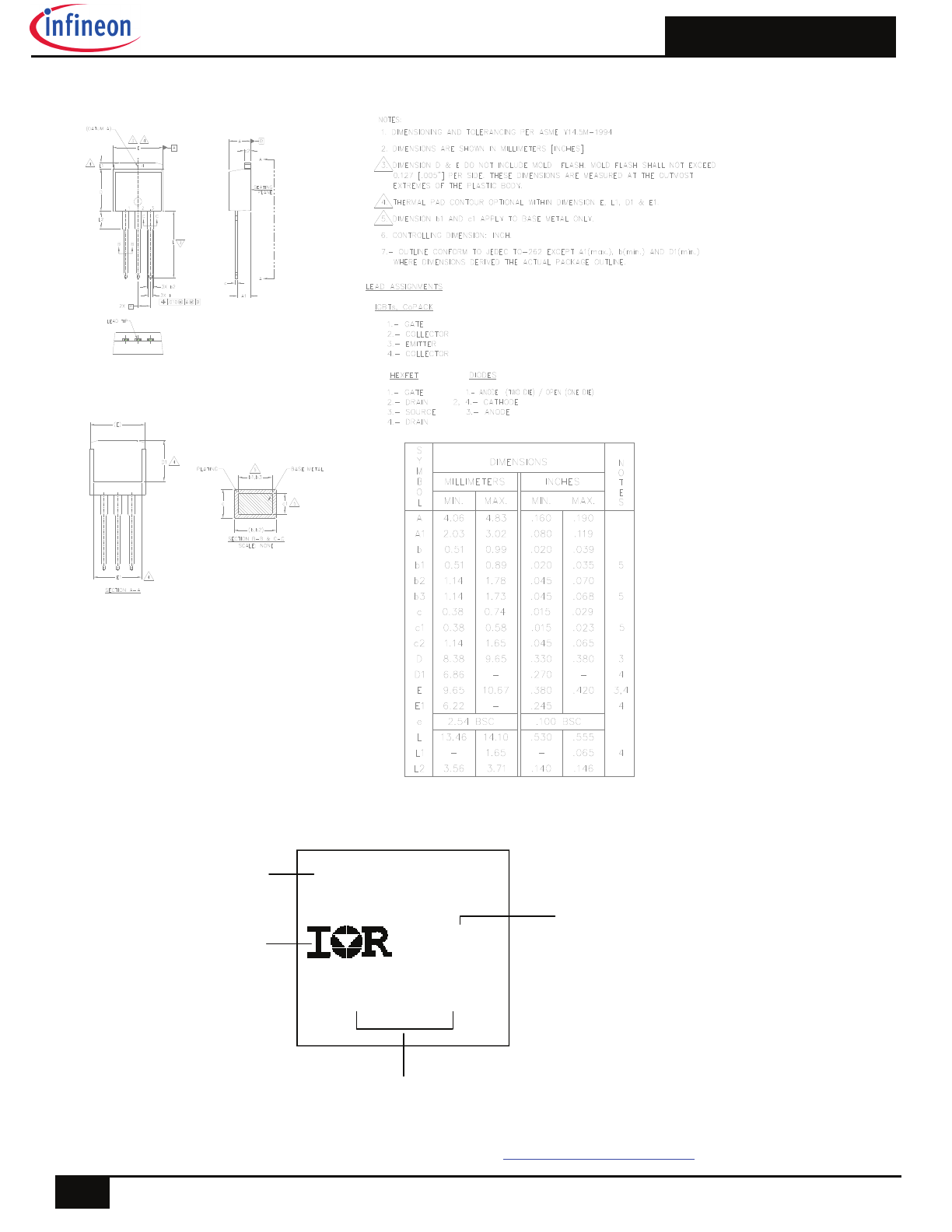
AUIRL1404S
TO-262
AUIRL1404L
S
D
G
S
D
G
D
Base part number
Package Type
Standard Pack
Form
Quantity
AUIRL1404L
TO-262
Tube
50
AUIRL1404L
AUIRL1404S
D
2
-Pak
Tube
50
AUIRL1404S
Tape and Reel Left
800
AUIRL1404STRL
Orderable Part Number
G D S
Gate Drain
Source
HEXFET
®
Power MOSFET
AUIRL1404S/L
2
2015-10-27
Notes:
Repetitive rating; pulse width limited by max. junction temperature. (See fig.11)
Limited by T
Jmax,
starting T
J
= 25°C, L = 0.35mH, R
G
= 25
, I
AS
= 95A, V
GS
=10V. (See fig.12)
I
SD
95A, di/dt 160A/µs, V
DD
V
(BR)DSS
, T
J
175°C.
Pulse width
300µs; duty cycle 2%.
C
oss eff
. is a fixed capacitance that gives the same charging time as C
oss
while V
DS
is rising from 0 to 80% V
DSS
.
Calculated continuous current based on maximum allowable junction temperature; for recommended current-handing of the
package refer to Design Tip # 93-4.
This is applied to D
2
Pak, When mounted on 1" square PCB (FR-4 or G-10 Material). For recommended footprint and soldering
techniques refer to application note #AN-994
Static @ T
J
= 25°C (unless otherwise specified)
Parameter Min.
Typ.
Max.
Units
Conditions
V
(BR)DSS
Drain-to-Source Breakdown Voltage
40
––– –––
V V
GS
= 0V, I
D
= 250µA
V
(BR)DSS
/
T
J
Breakdown Voltage Temp. Coefficient
––– 0.038 ––– V/°C Reference to 25°C, I
D
= 1mA
R
DS(on)
Static Drain-to-Source On-Resistance
––– ––– 4.0
m
V
GS
= 10V, I
D
= 95A
––– ––– 5.9
V
GS
= 4.3V, I
D
= 40A
V
GS(th)
Gate Threshold Voltage
1.0 –––
3.0
V V
DS
= V
GS
, I
D
= 250µA
gfs
Forward Trans conductance
93
––– –––
S V
DS
= 25V, I
D
= 95A
I
DSS
Drain-to-Source Leakage Current
––– ––– 20
µA
V
DS
= 40V, V
GS
= 0V
––– ––– 250
V
DS
= 32V,V
GS
= 0V,T
J
=150°C
I
GSS
Gate-to-Source Forward Leakage
––– ––– 200
nA
V
GS
= 20V
Gate-to-Source Reverse Leakage
––– ––– -200
V
GS
= -20V
Dynamic Electrical Characteristics @ T
J
= 25°C (unless otherwise specified)
Q
g
Total Gate Charge
––– ––– 140
nC
I
D
= 95A
Q
gs
Gate-to-Source Charge
––– –––
48
V
DS
= 32V
Q
gd
Gate-to-Drain Charge
––– –––
60
V
GS
= 5.0V, See Fig. 6
t
d(on)
Turn-On Delay Time
–––
18
–––
ns
V
DD
= 20V
t
r
Rise Time
––– 270 –––
I
D
= 95A
t
d(off)
Turn-Off Delay Time
–––
38
–––
R
G
= 2.5
V
GS
= 4.5V
t
f
Fall Time
––– 130 –––
R
D
= 0.25
L
D
Internal Drain Inductance
––– 4.5
–––
Between lead,
6mm (0.25in.)
L
S
Internal Source Inductance
––– 7.5
–––
from package
and center of die contact
C
iss
Input Capacitance
––– 6600 –––
pF
V
GS
= 0V
C
oss
Output Capacitance
––– 1700 –––
V
DS
= 25V
C
rss
Reverse Transfer Capacitance
––– 350 –––
ƒ = 1.0MHz, See Fig. 5
C
oss
Output Capacitance
––– 6700 –––
V
GS
= 0V, V
DS
= 1.0V ƒ = 1.0MHz
C
oss
Output Capacitance
––– 1500 –––
V
GS
= 0V, V
DS
= 32V ƒ = 1.0MHz
C
oss eff.
Effective Output Capacitance
––– 1500 –––
V
GS
= 0V, V
DS
= 0V to 32V
Diode Characteristics
Parameter
Min. Typ. Max. Units
Conditions
I
S
Continuous Source Current
––– ––– 160
A
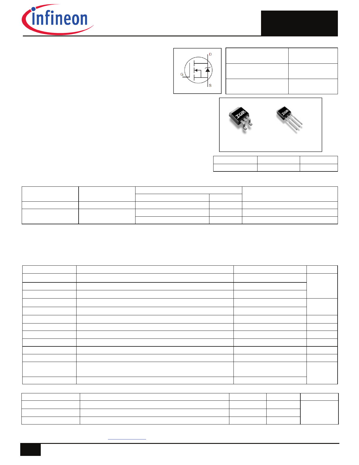
MOSFET symbol
(Body Diode)
showing the
I
SM
Pulsed Source Current
––– ––– 640
integral reverse
(Body Diode)
p-n junction diode.
V
SD
Diode Forward Voltage
––– –––
1.3
V T
J
= 25°C,I
S
= 95A,V
GS
= 0V
t
rr
Reverse Recovery Time
–––
63
94
ns T
J
= 25°C ,I
F
= 95A
Q
rr
Reverse Recovery Charge
––– 170 250
nC di/dt = 100A/µs
t
on
Forward Turn-On Time
Intrinsic turn-on time is negligible (turn-on is dominated by L
S
+L
D
)
nH
AUIRL1404S/L
3
2015-10-27
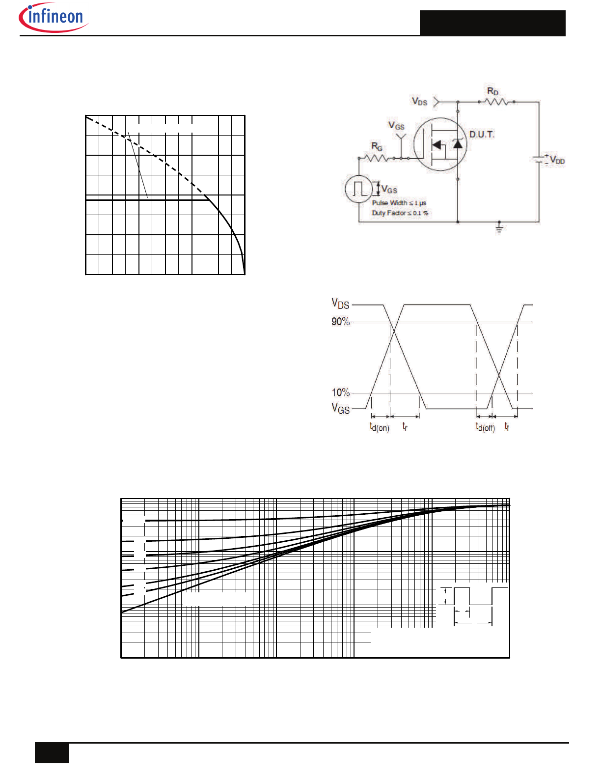
Fig. 2 Typical Output Characteristics
Fig. 3
Typical Transfer Characteristics
Fig. 1 Typical Output Characteristics
Fig. 4
Normalized On-Resistance vs. Temperature
10
100
1000
0.1
1
10
100
20µs PULSE WIDTH
T = 175 C
J
°
TOP
BOTTOM
VGS
15V
10V
8.0V
7.0V
6.0V
5.5V
5.0V
4.3V
V , Drain-to-Source Voltage (V)
I , Drain
-to-S
ource Current
(A
)
DS
D
4.3V
100
1000
4.0
5.0
6.0
7.0
8.0
V = 15V
20µs PULSE WIDTH
DS
V , Gate-to-Source Voltage (V)
I
, D
rai
n-
to-
S
our
ce C
ur
rent
(
A
)
GS
D
T = 25 C
J
°
T = 175 C
J
°
-60 -40 -20
0
20 40 60 80 100 120 140 160 180
0.0
0.5
1.0
1.5
2.0
2.5
T , Junction Temperature
( C)
R
,
D
rai
n-
to-
S
our
ce O
n
R
e
si
st
ance
(N
o
rm
a
lize
d)
J
D
S
(on)
°
V
=
I =
GS
D
10V
160A
10
100
1000
0.1
1
10
100
20µs PULSE WIDTH
T = 25 C
J
°
TOP
BOTTOM
VGS
15V
10V
8.0V
7.0V
6.0V
5.5V
5.0V
4.3V
V , Drain-to-Source Voltage (V)
I , Drain-to-Source Current (A)
DS
D
4.3V
AUIRL1404S/L
4
2015-10-27
Fig 5. Typical Capacitance vs. Drain-to-Source Voltage
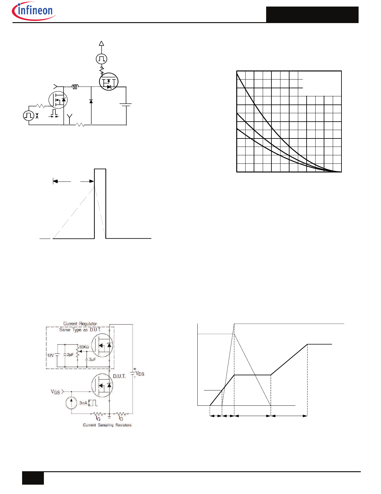
Fig 8. Maximum Safe Operating Area
Fig 6. Typical Gate Charge vs. Gate-to-Source Voltage
Fig. 7 Typical Source-to-Drain Diode
1
10
100
0
2000
4000
6000
8000
10000
V , Drain-to-Source Voltage (V)
C,
Ca
pa
ci
ta
nc
e
(p
F)
DS
V
C
C
C
=
=
=
=
0V,
C
C
C
f = 1MHz
+ C
+ C
C SHORTED
GS
iss
gs
gd ,
ds
rss
gd
oss
ds
gd
Ciss
Coss
Crss
0
100
200
300
400
500
0
4
8
12
16
20
Q , Total Gate Charge (nC)
V
,
G
at
e-
to-
Sour
ce
V
ol
tage
(
V
)
G
GS
FOR TEST CIRCUIT
SEE FIGURE
I =
D
13
95A
V
= 20V
DS
V
= 32V
DS
1
10
100
1000
0.0
0.5
1.0
1.5
2.0
2.5
3.0
V ,Source-to-Drain Voltage (V)
I
,
R
ever
se D
rai
n C
ur
rent
(
A
)
SD
SD
V = 0 V
GS
T = 25 C
J
°
T = 175 C
J
°
10
100
1000
10000
1
10
100
OPERATION IN THIS AREA LIMITED
BY R
DS(on)
Single Pulse
T
T
= 175 C
= 25 C
°
°
J
C
V , Drain-to-Source Voltage (V)
I
,
D
ra
in
C
u
rr
e
n
t (
A
)
I
,
D
ra
in
C
u
rr
e
n
t (
A
)
DS
D
10us
100us
1ms
10ms
AUIRL1404S/L
5
2015-10-27
Fig 11. Maximum Effective Transient Thermal Impedance, Junction-to-Case
Fig 9. Maximum Drain Current vs.
Case Temperature
Fig 10a. Switching Time Test Circuit
Fig 10b. Switching Time Waveforms
25
50
75
100
125
150
175
0
40
80
120
160
T , Case Temperature
( C)
I
, D
ra
in
C
urre
nt
(A
)
°
C
D
LIMITED BY PACKAGE
0.001
0.01
0.1
1
0.00001
0.0001
0.001
0.01
0.1
1
Notes:
1. Duty factor D =
t / t
2. Peak T = P
x Z
+ T
1
2
J
DM
thJC
C
P
t
t
DM
1
2
t , Rectangular Pulse Duration (sec)
T
he
rma
l R
e
sp
on
se
(Z
)
1
th
JC
0.01
0.02
0.05
0.10
0.20
D = 0.50
SINGLE PULSE
(THERMAL RESPONSE)
AUIRL1404S/L
6
2015-10-27
Fig 12c. Maximum Avalanche Energy vs. Drain Current
R G
IAS
0.01
tp
D.U.T
L
VDS
+
- VDD
DRIVER
A
15V
20V
Fig 12a. Unclamped Inductive Test Circuit
tp
V
(BR)DSS
I
AS
Fig 12b. Unclamped Inductive Waveforms
Fig 13a. Gate Charge Test Circuit
Vds
Vgs
Id
Vgs(th)
Qgs1 Qgs2
Qgd
Qgodr
Fig 13b. Gate Charge Waveform
25
50
75
100
125
150
175
0
200
400
600
800
1000
1200
Starting T , Junction Temperature
( C)
E ,
S
in
g
le Puls
e
A
valan
che
En
er
gy (mJ
)
J
AS
°
ID
TOP
BOTTOM
39A
67A
95A
AUIRL1404S/L
7
2015-10-27
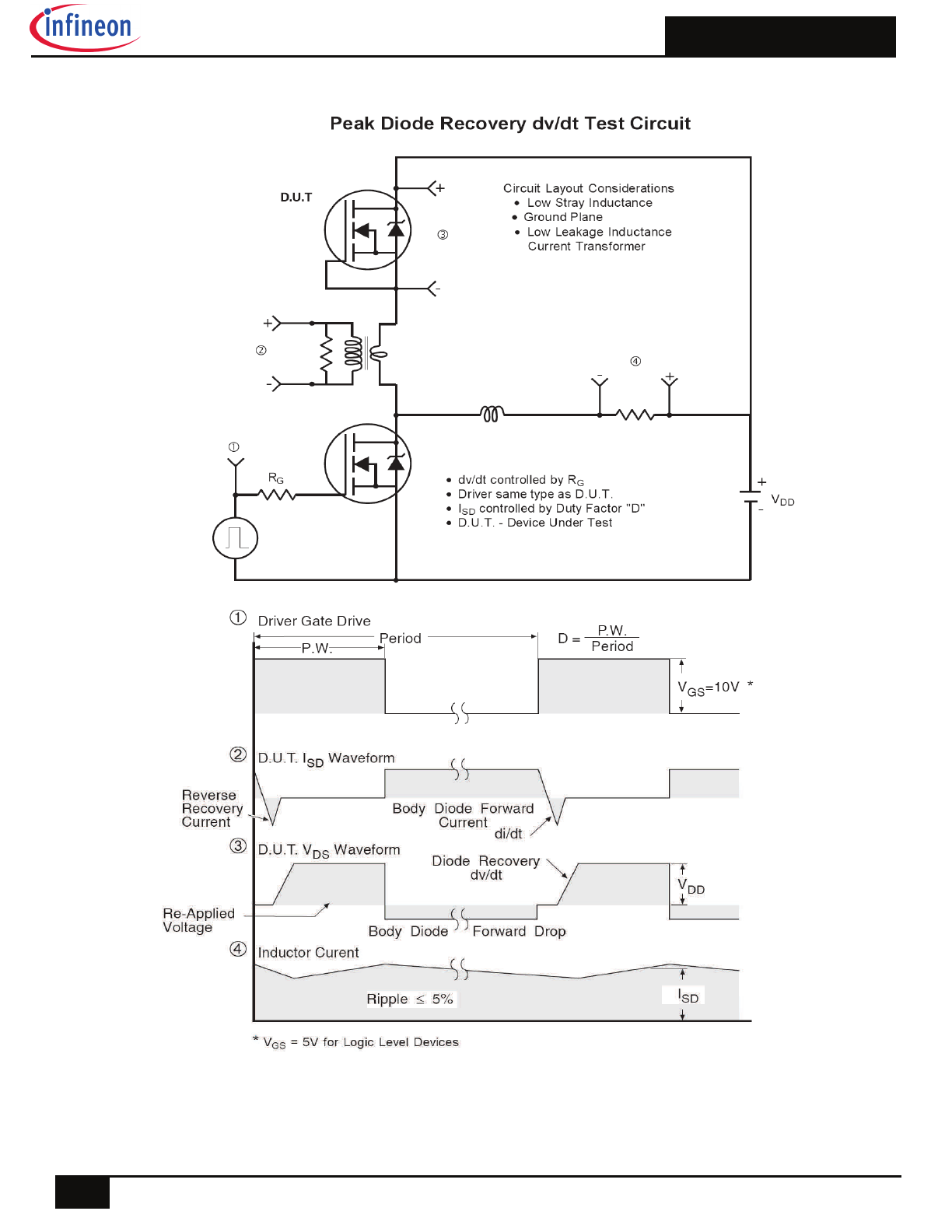
Fig 14. Peak Diode Recovery dv/dt Test Circuit for N-Channel HEXFET® Power MOSFETs
AUIRL1404S/L
8
2015-10-27
Note: For the most current drawing please refer to IR website at
http://www.irf.com/package/
D
2
Pak (TO-263AB) Part Marking Information
YWWA
XX
XX
Date Code
Y= Year
WW= Work Week
AUL1404S
Lot Code
Part Number
IR Logo
D
2
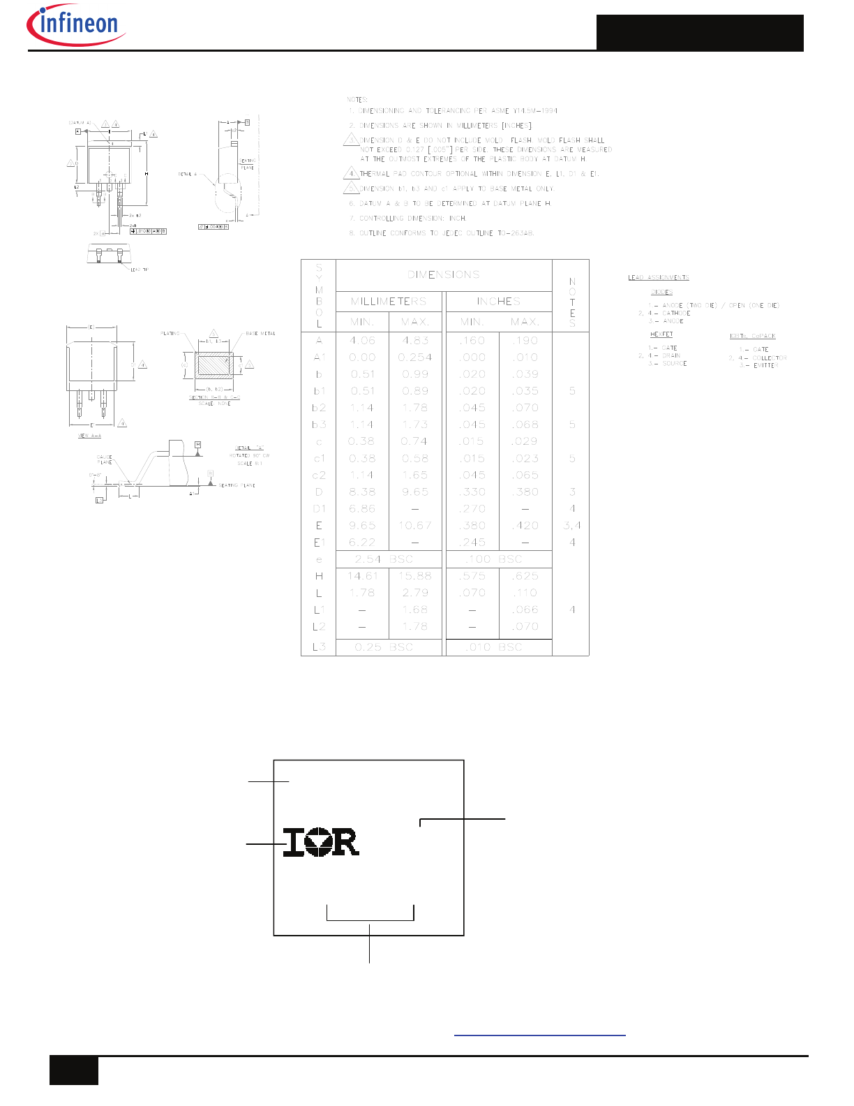
Pak (TO-263AB) Package Outline (Dimensions are shown in millimeters (inches))
AUIRL1404S/L
9
2015-10-27
TO-262 Part Marking Information
YWWA
XX
XX
Date Code
Y= Year
WW= Work Week
AUL1404L
Lot Code
Part Number
IR Logo
TO-262 Package Outline (Dimensions are shown in millimeters (inches)
Note: For the most current drawing please refer to IR website at
http://www.irf.com/package/
AUIRL1404S/L
10
2015-10-27
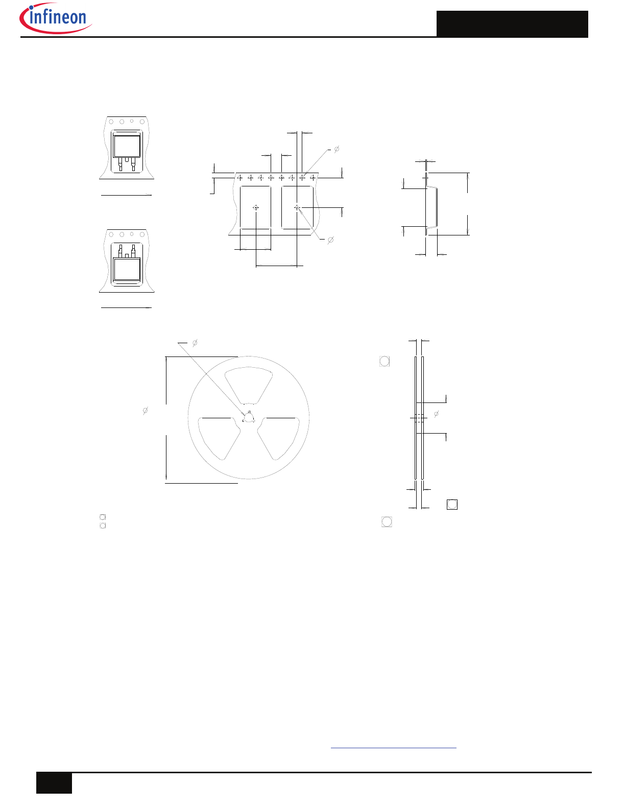
D
2
Pak (TO-263AB) Tape & Reel Information (Dimensions are shown in millimeters (inches))
Note: For the most current drawing please refer to IR website at
http://www.irf.com/package/
3
4
4
TRR
FEED DIRECTION
1.85 (.073)
1.65 (.065)
1.60 (.063)
1.50 (.059)
4.10 (.161)
3.90 (.153)
TRL
FEED DIRECTION
10.90 (.429)
10.70 (.421)
16.10 (.634)
15.90 (.626)
1.75 (.069)
1.25 (.049)
11.60 (.457)
11.40 (.449)
15.42 (.609)
15.22 (.601)
4.72 (.136)
4.52 (.178)
24.30 (.957)
23.90 (.941)
0.368 (.0145)
0.342 (.0135)
1.60 (.063)
1.50 (.059)
13.50 (.532)
12.80 (.504)
330.00
(14.173)
MAX.
27.40 (1.079)
23.90 (.941)
60.00 (2.362)
MIN.
30.40 (1.197)
MAX.
26.40 (1.039)
24.40 (.961)
NOTES :
1. COMFORMS TO EIA-418.
2. CONTROLLING DIMENSION: MILLIMETER.
3. DIMENSION MEASURED @ HUB.
4. INCLUDES FLANGE DISTORTION @ OUTER EDGE.