
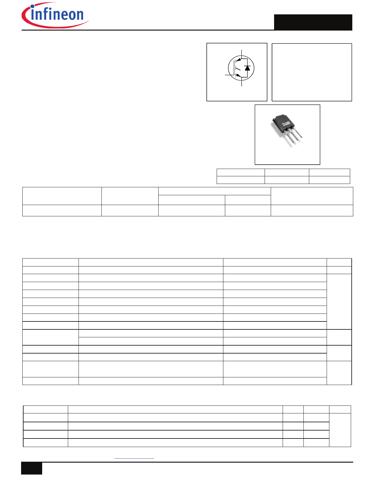
AUIRGPS4067D1
G C E
Gate Collector
Emitter
AUTOMOTIVE GRADE
Parameter Max.
Units
V
CES
Collector-to-Emitter Voltage
600
V
I
C
@ T
C
= 25°C
Continuous Collector Current
240
A
I
C
@ T
C
= 100°C
Continuous Collector Current
160
I
NOMINAL
Nominal
Current
120
I
CM
Pulse Collector Current, V
GE
= 15V
360
I
LM
Clamped Inductive Load Current, V
GE
= 20V 480
I
F
NOMINAL
Diode Nominal Current 120
I
FM
Diode Maximum Forward Current 480
V
GE
Continuous Gate-to-Emitter Voltage
±20
V
Transient Gate-to-Emitter Voltage
±30
P
D
@ T
C
= 25°C
Maximum Power Dissipation
750
W
P
D
@ T
C
= 100°C
Maximum Power Dissipation
375
T
J
Operating Junction and
-55 to +175
T
STG
Storage Temperature Range
Soldering Temperature, for 10 sec.
300 (0.063 in. (1.6mm) from case)
°C
Absolute Maximum Ratings
Stresses beyond those listed under “Absolute Maximum Ratings” may cause permanent damage to the device. These are stress rat-
ings only; and functional operation of the device at these or any other condition beyond those indicated in the specifications is not
implied. Exposure to absolute-maximum-rated conditions for extended periods may affect device reliability. The thermal resistance
and power dissipation ratings are measured under board mounted and still air conditions. Ambient temperature (T
A
) is 25°C, unless
otherwise specified.
E
G
n-channel
C
Base Part Number
Package Type
Standard Pack
Orderable Part Number
Form
Quantity
AUIRGPS4067D1 PG-TO274-3-903
Tube
25
AUIRGPS4067D1
1
2018-07-19
PG-TO274-3-903
*
Qualification standards can be found at
www.infineon.com
INSULATED GATE BIPOLAR TRANSISTOR WITH ULTRAFAST SOFT RECOVERY DIODE
Thermal Resistance
Parameter
Typ. Max.
Units
R
JC
(IGBT)
Thermal Resistance Junction-to-Case (each IGBT)
––– 0.20
R
JC
(Diode)
Thermal Resistance Junction-to-Case (each Diode)
––– 0.44
R
CS
Thermal Resistance, Case-to-Sink (flat, greased surface)
0.24 –––
R
JA
Thermal Resistance, Junction-to-Ambient (typical socket mount)
––– 40
°C/W
Features
Low V
CE (on)
Trench IGBT Technology
Low Switching Losses
6µs SCSOA
Square RBSOA
100% of the parts tested for I
LM
Positive V
CE (on)
Temperature Coefficient
Soft Recovery Co-pak Diode
Lead-Free, RoHS Compliant
Automotive Qualified *
Benefits
High Efficiency in a Wide Range of Applications
Suitable for Applications in the Low to Mid-Range Frequencies
Rugged Transient Performance for Increased Reliability
Excellent Current Sharing in Parallel Operation
Low EMI
V
CES
= 600V
I
C
= 160A
,
T
C
= 100°C
tsc
6µs, T
J(MAX)
= 175°C
V
CE(on) typ
. = 1.70V
C E
G
C
AUIRGPS4067D1
2
2018-07-19
Electrical Characteristics @ T
J
= 25°C (unless otherwise specified)
Parameter
Min. Typ. Max. Units
Conditions
V
(BR)CES
Collector-to-Emitter Breakdown Voltage
600 — — V
V
GE
= 0V, I
C
= 500µA
V
(BR)CES
/
T
J
Temperature Coeff. of Breakdown Voltage
— 0.27 — V/°C
V
GE
= 0V, I
C
= 15mA (25°C-175°C)
V
CE(on)
Collector-to-Emitter Saturation Voltage
— 1.7
2.05
V
I
C
= 120A, V
GE
= 15V, T
J
= 25°C
— 2.15 —
I
C
= 120A, V
GE
= 15V, T
J
= 150°C
— 2.20 —
I
C
= 120A, V
GE
= 15V, T
J
= 175°C
V
GE(th)
Gate Threshold Voltage
4.0 — 6.5 V
V
CE
= V
GE
, I
C
= 5.6mA
V
GE(th)
/
TJ Threshold Voltage temp. coefficient
— -17 —
mV/°C
V
CE
= V
GE
, I
C
= 20mA (25°C-175°C)
gfe
Forward Transconductance
— 85 — S
V
CE
= 50V, I
C
= 120A
Collector-to-Emitter Leakage Current
— 2.3
200 µA
V
GE
= 0V, V
CE
= 600V
— 9.4 — mA V
GE
= 0V, V
CE
= 600V,T
J
= 175°C
V
FM
Diode Forward Voltage Drop
— 1.9 2.2
V
I
F
= 120A
— 2.0 —
I
F
= 120A, T
J
= 175°C
I
GES
Gate-to-Emitter Leakage Current
— —
±100
nA
V
GE
= ±20V
I
CES
Switching Characteristics @ T
J
= 25°C (unless otherwise specified)
Parameter Min.
Typ.
Max.
Units
Conditions
Q
g
Total Gate Charge (turn-on)
—
240
360
nC
I
C
= 120A
Q
ge
Gate-to-Emitter Charge (turn-on)
—
69
104
V
GE
= 15V
Q
gc
Gate-to-Collector Charge (turn-on)
—
90
135
V
CC
= 400V
E
on
Turn-On Switching Loss
—
8.2
10
mJ
E
off
Turn-Off Switching Loss
—
2.9
3.2
E
total
Total Switching Loss
—
11.1 13.2
I
C
= 120A, V
CC
= 400V, V
GE
= 15V
t
d(on)
Turn-On delay time
—
69
82
ns
R
G
= 4.7
, L = 87µH, T
J
= 25°C
t
r
Rise time
—
65
82
Energy losses include tail & diode
t
d(off)
Turn-Off delay time
—
198
230
reverse recovery
t
f
Fall time
—
38
48
E
on
Turn-On Switching Loss
—
10
—
mJ
E
off
Turn-Off Switching Loss
—
3.8
—
E
total
Total Switching Loss
—
13.8
—
I
C
= 120A, V
CC
= 400V, V
GE
= 15V
t
d(on)
Turn-On delay time
—
63
—
ns
R
G
= 4.7
, L = 87µH, T
J
= 175°C
t
r
Rise time
—
64
—
Energy losses include tail & diode
t
d(off)
Turn-Off delay time
—
230
—
reverse recovery
t
f
Fall time
—
51
—
C
ies
Input Capacitance
—
7780
—
pF
V
GE
= 0V
C
oes
Output Capacitance
—
505
—
V
CC
= 30V
C
res
Reverse Transfer Capacitance
—
245
—
f = 1.0Mhz
T
J
= 175°C, I
C
= 480A
RBSOA
Reverse Bias Safe Operating Area
FULL SQUARE
V
CC
= 480V, Vp ≤ 600V
Rg = 4.7
, V
GE
= +20V to 0V
SCSOA
Short Circuit Safe Operating Area
6
—
—
V
CC
= 400V, Vp ≤ 600V
Rg = 1.0
, V
GE
= +15V to 0V
Erec
Reverse Recovery Energy of the Diode
—
2440
—
µJ T
J
= 175°C
t
rr
Diode Reverse Recovery Time
—
360
—
ns V
CC
= 400V, I
F
= 120A
I
rr
Peak Reverse Recovery Current
—
53
—
A
V
GE
= 15V, Rg = 4.7
, L = 87µH
µs
Notes:
V
CC
= 80% (V
CES
), V
GE
= 20V, L = 0.87µH, R
G
= 50
tested in production ILM 400A.
Pulse width limited by max. junction temperature.
Refer to AN-1086 for guidelines for measuring V
(BR)CES
safely.
R
is measured at T
J
approximately 90°C.
Calculated continuous current based on maximum allowable junction temperature. Package IGBT current limit is 195A.
Package diode current limit is120A. Note that current limitations arising from heating of the device leads may occur.
AUIRGPS4067D1
3
2018-07-19
0
20 40 60 80 100 120 140 160 180
TC (°C)
0
100
200
300
400
500
600
700
800
P
to
t (
W
)
25
50
75
100
125
150
175
TC (°C)
0
50
100
150
200
250
I C
(
A
)
1
10
100
1000
10000
VCE (V)
0.1
1
10
100
1000
I C
(
A
)
1msec
10µsec
100µsec
Tc = 25°C
Tj = 175°C
Single Pulse
DC
0
1
2
3
4
5
6
7
8
9
10
VCE (V)
0
60
120
180
240
300
360
420
480
I C
E
(
A
)
VGE = 18V
VGE = 15V
VGE = 12V
VGE = 10V
VGE = 8.0V
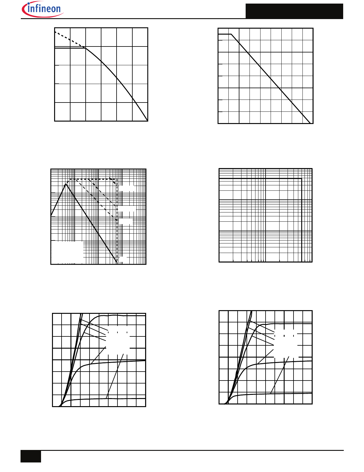
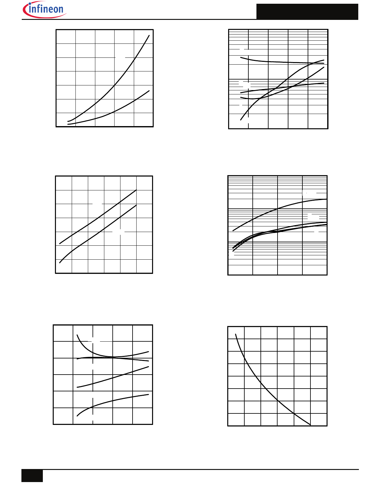
Fig. 3 - Forward SOA
T
C
= 25°C, T
J
175°C; V
GE
=15V
Fig. 1 - Maximum DC Collector Current vs.
Case Temperature
10
100
1000
VCE (V)
1
10
100
1000
I C
A
)
Fig. 4 - Reverse Bias SOA
T
J
= 175°C; V
GE
= 20V
Fig. 2 - Power Dissipation vs.
Case Temperature
Fig. 5 - Typ. IGBT Output Characteristics
T
J
= -40°C; tp = 30µs
0
1
2
3
4
5
6
7
8
9
10
VCE (V)
0
60
120
180
240
300
360
420
480
I C
E
(
A
)
VGE = 18V
VGE = 15V
VGE = 12V
VGE = 10V
VGE = 8.0V
Fig. 6 - Typ. IGBT Output Characteristics
T
J
= 25°C; tp = 30µs
AUIRGPS4067D1
4
2018-07-19
0
1
2
3
4
5
6
7
8
9
10
VCE (V)
0
60
120
180
240
300
360
420
480
I C
E
(
A
)
VGE = 18V
VGE = 15V
VGE = 12V
VGE = 10V
VGE = 8.0V
0.0
1.0
2.0
3.0
4.0
5.0
VF (V)
0
60
120
180
240
300
360
420
480
I F
(
A
)
TJ = -40°C
TJ = 25°C
TJ =175°C
5
10
15
20
VGE (V)
0
2
4
6
8
10
V
C
E
(
V
)
ICE = 60A
ICE = 120A
ICE = 195A
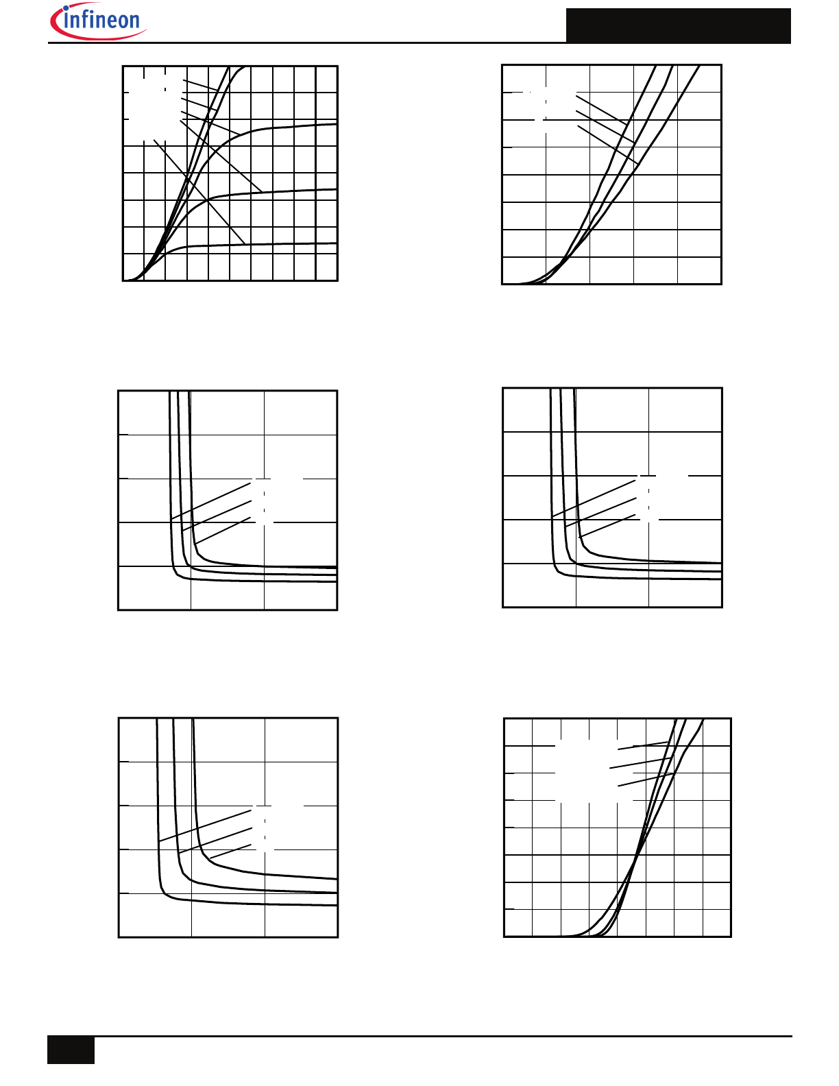
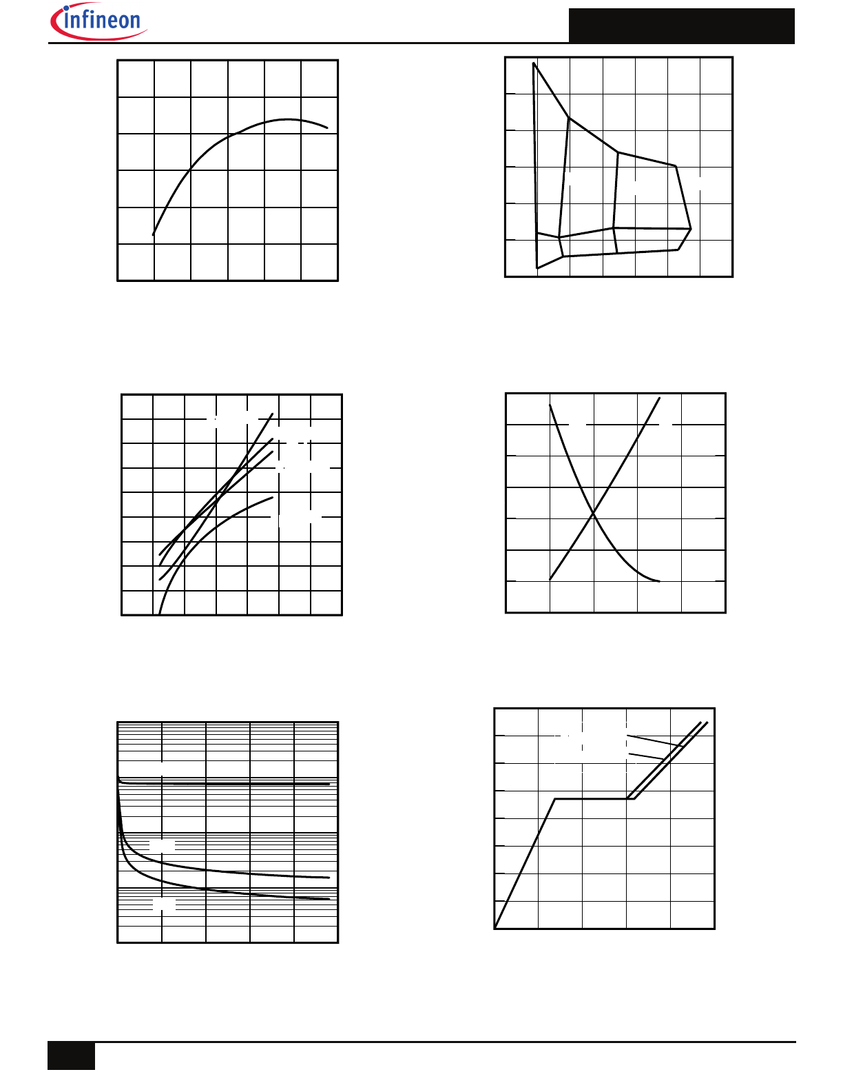
Fig. 7 - Typ. IGBT Output Characteristics
T
J
= 175°C; tp = 30µs
5
10
15
20
VGE (V)
0
2
4
6
8
10
V
C
E
(
V
)
ICE = 60A
ICE = 120A
ICE = 195A
Fig. 8 - Typ. Diode Forward Characteristics
tp = 30µs
5
10
15
20
VGE (V)
0
2
4
6
8
10
V
C
E
(
V
)
ICE = 60A
ICE = 120A
ICE = 195A
Fig. 11 - Typical V
CE
vs. V
GE
T
J
= 175°C
Fig. 9 - Typical V
CE
vs. V
GE
T
J
= -40°C
0
2
4
6
8
10
12
14
16
VGE, Gate-to-Emitter Voltage (V)
0
60
120
180
240
300
360
420
480
I C
,
C
ol
le
ct
or
-t
o-
E
m
itt
er
C
ur
re
nt
(
A
)
TJ = -40°C
TJ = 25°C
TJ = 175°C
Fig. 12 - Typ. Transfer Characteristics
V
CE
= 50V; tp = 10µs
Fig. 10 - Typical V
CE
vs. V
GE
T
J
= 25°C
AUIRGPS4067D1
5
2018-07-19
0
20
40
60
80
100
120
RG ()
0
5000
10000
15000
20000
25000
30000
35000
E
ne
rg
y
(µ
J)
EOFF
EON
Fig. 15 - Typ. Energy Loss vs. R
G
T
J
= 175°C; L = 0.087mH; V
CE
= 400V, I
CE
= 120A; V
GE
= 15V
0
50
100
150
200
250
IC (A)
10
100
1000
S
w
ic
hi
ng
T
im
e
(n
s)
tR
tdOFF
tF
tdON
0
50
100
150
200
250
IC (A)
0
5000
10000
15000
20000
25000
30000
35000
E
ne
rg
y
(µ
J)
EOFF
EON
Fig. 13 - Typ. Energy Loss vs. I
C
T
J
= 175°C; L = 0.087mH; V
CE
= 400V, R
G
= 5.0
; V
GE
= 15V
0
25
50
75
100
RG ()
10
100
1000
10000
S
w
ic
hi
ng
T
im
e
(n
s)
tR
tdOFF
tF
tdON
Fig. 16 - Typ. Switching Time vs. R
G
T
J
= 175°C; L = 0.087mH; V
CE
= 400V, I
CE
= 120A; V
GE
= 15V
Fig. 14 - Typ. Switching Loss vs. I
C
T
J
= 175°C; L = 0.087mH; V
CE
= 400V, R
G
= 5.0
; V
GE
= 15V
0
50
100
150
200
250
IF (A)
30
35
40
45
50
55
60
I R
R
(
A
)
RG = 10
RG = 2
RG = 4.7
RG = 50
Fig. 17 - Typ. Diode I
RR
vs. I
F
T
J
= 175°C
0
10
20
30
40
50
60
RG (
36
38
40
42
44
46
48
50
52
I R
R
(
A
)
Fig. 18 - Typ. Diode I
RR
vs. R
G
T
J
= 175°C
AUIRGPS4067D1
6
2018-07-19
Fig. 24 - Typical Gate Charge vs. V
GE
I
CE
= 120A
0
100
200
300
400
500
VCE (V)
10
100
1000
10000
100000
C
ap
ac
ita
nc
e
(p
F
)
Cies
Coes
Cres
Fig. 23 - Typ. Capacitance vs. V
CE
V
GE
= 0V; f = 1MHz
Fig. 21 - Typ. Diode E
RR
vs. I
F
T
J
= 175°C
8
10
12
14
16
18
VGE (V)
4
6
8
10
12
14
16
18
T
im
e
(
µs
)
200
300
400
500
600
700
800
900
C
u
rre
nt
(A
)
Tsc
Isc
0
50
100
150
200
250
Q G, Total Gate Charge (nC)
0
2
4
6
8
10
12
14
16
V
G
E
, G
at
e-
to
-E
m
itt
er
V
ol
ta
ge
(
V
)
VCES = 400V
VCES = 300V
Fig. 22 - V
GE
vs. Short Circuit Time
V
CC
= 400V; T
C
= 25°C
Fig. 20 - Typ. Diode Q
RR
vs. diF/dt
V
CC
= 400V; V
GE
= 15V; T
J
= 175°C
200
400
600
800
1000
1200
1400
diF /dt (A/µs)
30
35
40
45
50
55
60
I R
R
(
A
)
200
400
600
800 1000 1200 1400 1600
diF /dt (A/µs)
5000
10000
15000
20000
25000
30000
35000
Q
R
R
(
nC
)
10
2
50
4.7
120A
240A
60A
0
50
100
150
200
250
300
350
IF (A)
1000
1500
2000
2500
3000
3500
4000
4500
5000
5500
E
ne
rg
y
(µ
J)
RG = 10
RG = 20
RG = 4.7
RG = 50
Fig. 19 - Typ. Diode I
RR
vs. diF/dt
V
CC
= 400V; V
GE
= 15V; I
F
= 120A; T
J
= 175°C
AUIRGPS4067D1
7
2018-07-19
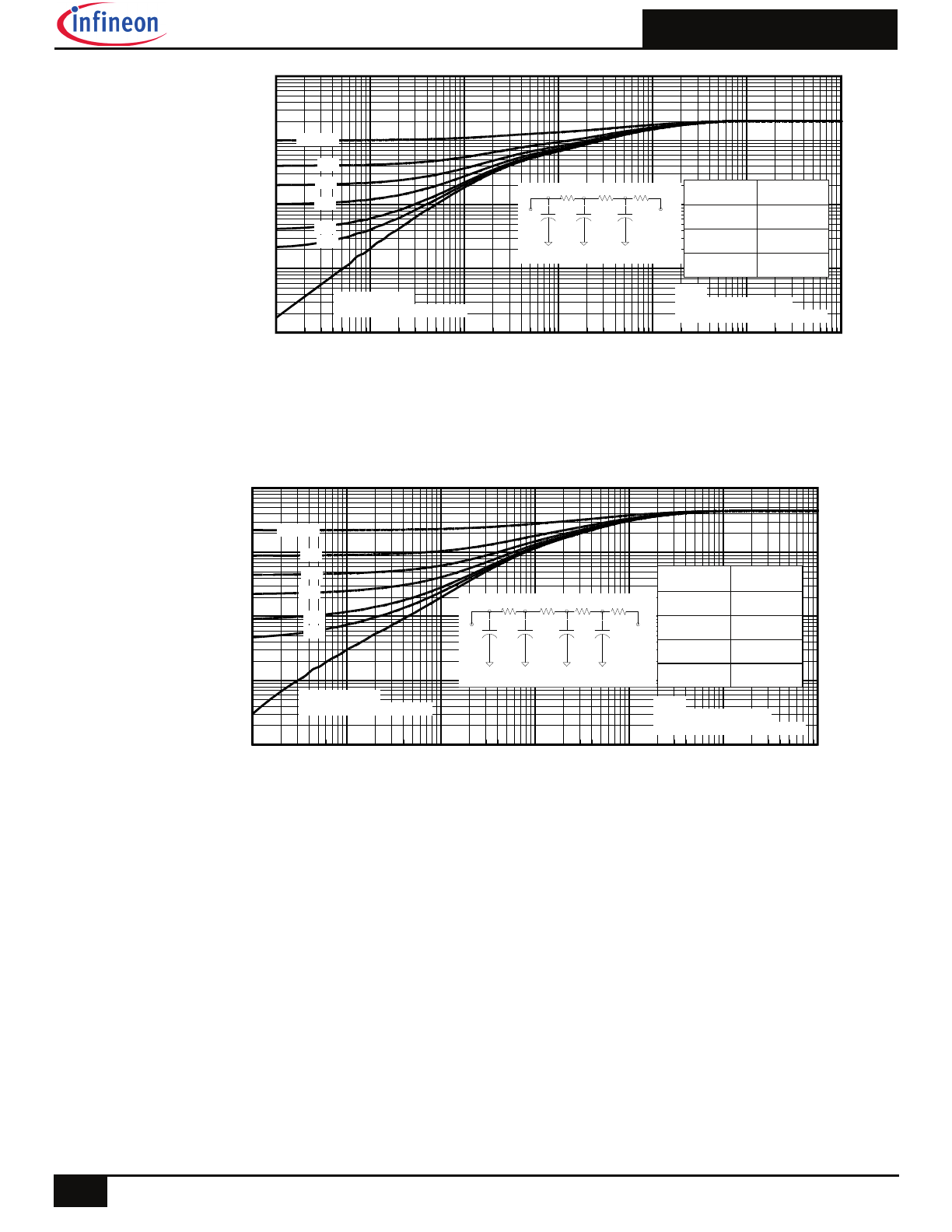
Fig 26. Maximum Transient Thermal Impedance, Junction-to-Case (DIODE)
Fig 25. Maximum Transient Thermal Impedance, Junction-to-Case (IGBT)
1E-006
1E-005
0.0001
0.001
0.01
0.1
1
t1 , Rectangular Pulse Duration (sec)
0.0001
0.001
0.01
0.1
1
T
he
rm
al
R
es
po
ns
e
(
Z
th
JC
)
0.20
0.10
D = 0.50
0.02
0.01
0.05
SINGLE PULSE
( THERMAL RESPONSE )
Notes:
1. Duty Factor D = t1/t2
2. Peak Tj = P dm x Zthjc + Tc
Ri (°C/W)
I (sec)
0.0564
0.000253
0.0888
0.003155
0.0547
0.014893
J
J
1
1
2
2
3
3
R
1
R
1
R
2
R
2
R
3
R
3
C
C
Ci=
iRi
Ci=
iRi
1E-006
1E-005
0.0001
0.001
0.01
0.1
1
t1 , Rectangular Pulse Duration (sec)
0.0001
0.001
0.01
0.1
1
T
he
rm
al
R
es
po
ns
e
(
Z
th
JC
)
0.20
0.10
D = 0.50
0.02
0.01
0.05
SINGLE PULSE
( THERMAL RESPONSE )
Notes:
1. Duty Factor D = t1/t2
2. Peak Tj = P dm x Zthjc + Tc
J
J
1
1
2
2
3
3
R
1
R
1
R
2
R
2
R
3
R
3
Ci=
iRi
Ci=
iRi
C
C
4
4
R
4
R
4
Ri (°C/W)
I (sec)
0.00597
0.000016
0.14039
0.000387
0.19117
0.004096
0.10156
0.021245
AUIRGPS4067D1
8
2018-07-19
0
1K
VCC
DUT
L
Gate Charge Circuit
L
Rg
80 V
DUT
VCC
+
-
RBSOA Circuit
Fig.C.T.1 - Gate Charge Circuit (turn-off)
Fig.C.T.2 - RBSOA Circuit
L
Rg
VCC
DUT /
DRIVER
diode clamp /
DUT
-5V
Switching Loss
Rg
VCC
DUT
R =
VCC
ICM
Fig.C.T.4 - Switching Loss Circuit
Fig.C.T.5 - Resistive Load Circuit
DC
4X
DUT
VCC
R
SH
Fig.C.T.3 - S.C. SOA Circuit
G force
C sense
100K
DUT
0.0075µF
D1
22K
E force
C force
E sense
Fig.C.T.6 - BVCES Filter Circuit
AUIRGPS4067D1
9
2018-07-19
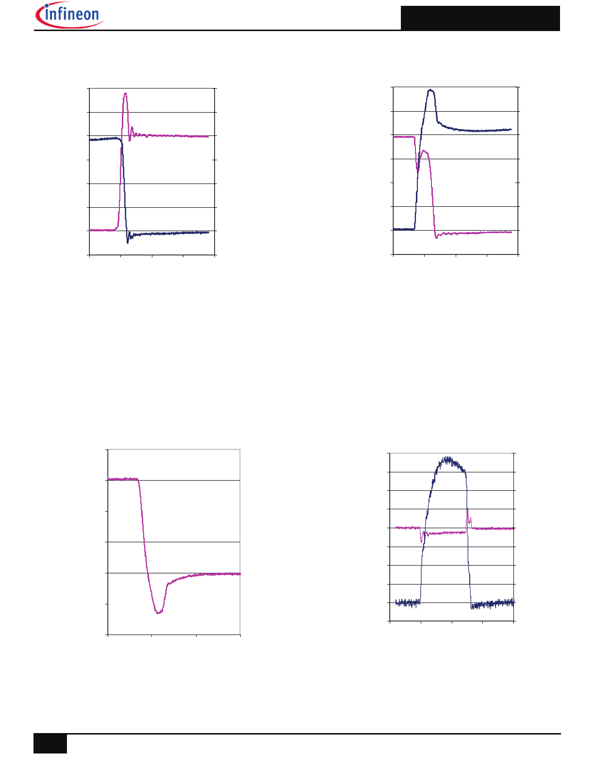
Fig. WF1 - Typ. Turn-off Loss Waveform
@ T
J
= 175°C using Fig. CT.4
Fig. WF2 - Typ. Turn-on Loss Waveform
@ T
J
= 175°C using Fig. CT.4
Fig. WF4 - Typ. S.C. Waveform
@ T
J
= 25°C using Fig. CT.3
Fig. WF3 - Typ. Diode Recovery Waveform
@ T
J
= 175°C using Fig. CT.4
-100
0
100
200
300
400
500
600
-50E-8 00E+0
50E-8
1E-6
2E-6
time(µs)
V
CE
(V
)
-30
0
30
60
90
120
150
180
I
CE
(A
)
V
CE
I
CE
-100
0
100
200
300
400
500
600
-5E-7
0E+0
5E-7
1E-6
2E-6
time (µs)
V
CE
(V
)
-30
0
30
60
90
120
150
180
I
CE
(A
)
V
CE
I
CE
-80
-40
0
40
80
120
160
-5.0E-7
0.0E+0
5.0E-7
1.0E-6
time (ns)
I
F
(A
)
-100
0
100
200
300
400
500
600
700
800
-5.0E-6 0.0E+0 5.0E-6 1.0E-5
1.5E-5
time (µs)
Vce
(
V
)
-100
0
100
200
300
400
500
600
700
800
Ic
e (
A
)
V
CE
I
CE
AUIRGPS4067D1
10
2018-07-19
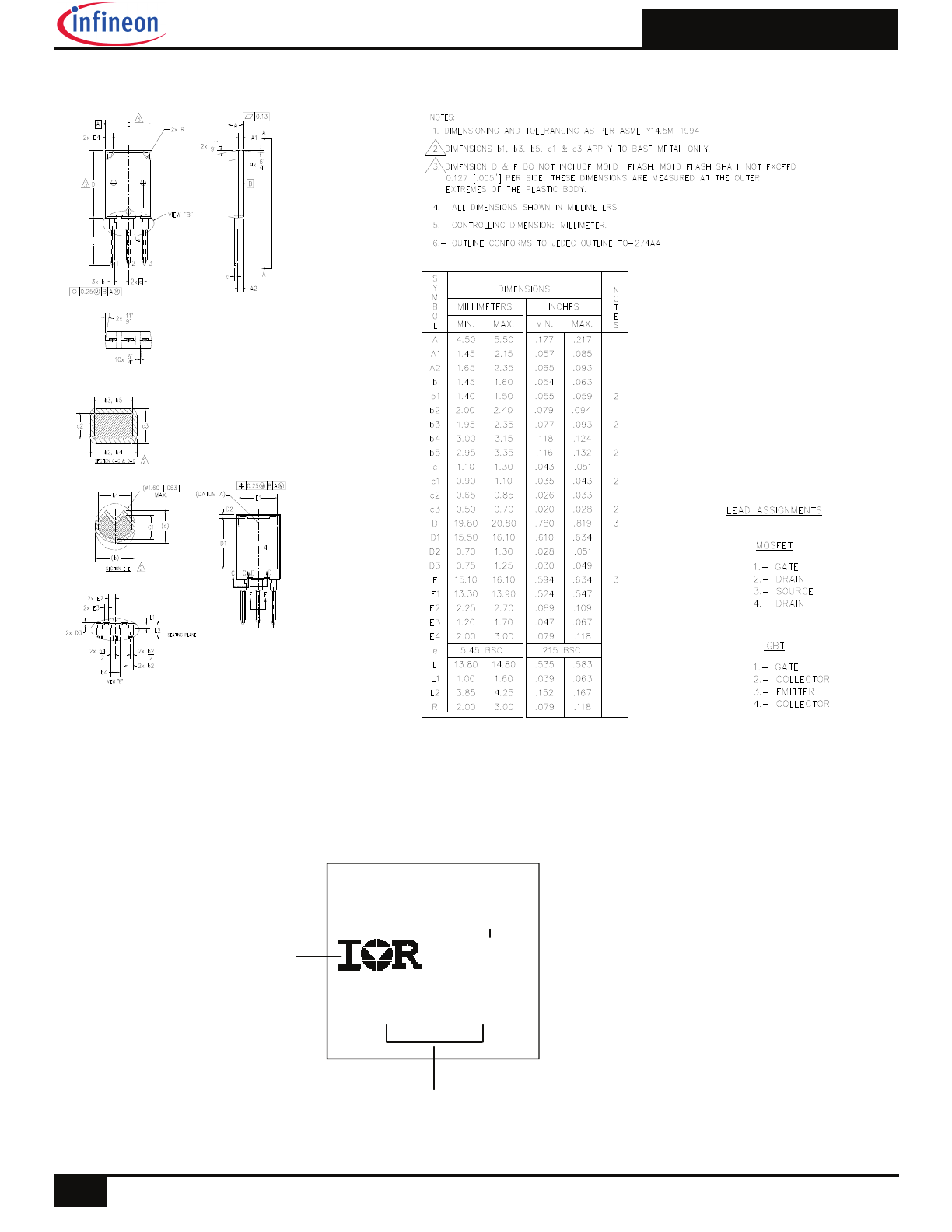
Case Outline and Dimensions-PG-TO274-3-903
Dimensions are shown in millimeters (inches))
PG-TO274-3-903 -Part Marking Information
YWWA
XX
XX
Date Code
Y = Year
WW = Work Week
A = Automotive, Lead Free
AUPS4067D1
Lot Code
Part Number
IR Logo