
INSULATED GATE BIPOLAR TRANSISTOR WITH
ULTRAFAST SOFT RECOVERY DIODE
V
CES
= 600V
I
C(Nominal)
= 24A
t
SC
≥ 5μs, T
J(max)
= 175°C
V
CE(on)
typ. = 1.57V
Features
•
Low V
CE (on)
Trench IGBT Technology
•
Low Switching Losses
•
5μs SCSOA
•
Square RBSOA
•
100% of The Parts Tested for I
LM
•
Positive V
CE (on)
Temperature Coefficient.
•
Ultra Fast Soft Recovery Co-pak Diode
•
Tighter Distribution of Parameters
•
Lead-Free, RoHS Compliant
•
Automotive Qualified *
Benefits
•
High Efficiency in a Wide Range of Applications
•
Suitable for a Wide Range of Switching Frequencies due
to Low V
CE (ON)
and Low Switching Losses
•
Rugged Transient Performance for Increased Reliability
•
Excellent Current Sharing in Parallel Operation
•
Low EMI
Absolute Maximum Ratings
Stresses beyond those listed under “Absolute Maximum Ratings” may cause permanent damage to the device. These are stress ratings only; and functional
operation of the device at these or any other condition beyond those indicated in the specifications is not implied.Exposure to absolute-maximum-rated
conditions for extended periods may affect device reliability. The thermal resistance and power dissipation ratings are measured under board mounted
and
still air conditions. Ambient temperature (T
A
) is 25
°C, unless otherwise specified
*Qualification standards can be found at http://www.irf.com/
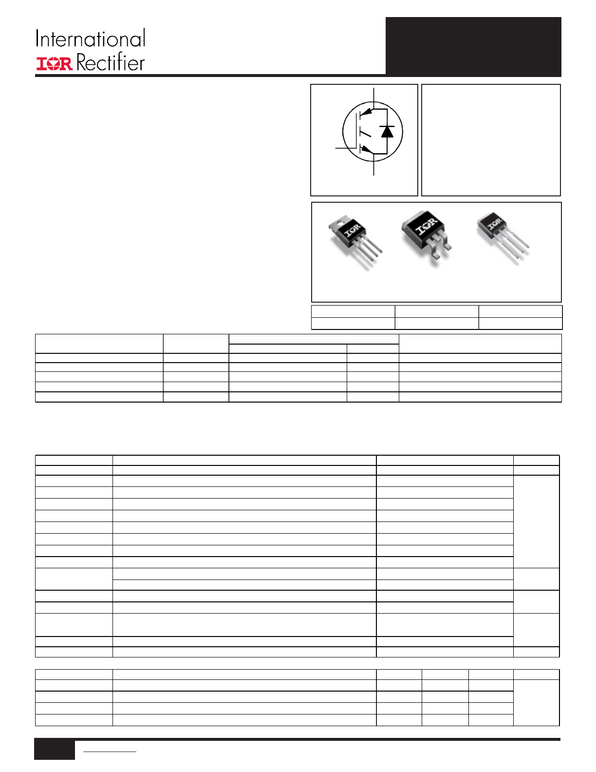
TO-220AB
AUIRGB4062D1
E
G
n-channel
C
Applications
•
Air Conditioning Compressor
D
2
Pak
AUIRGS4062D1
C
E
G
G
C
E
Gate
Collector
Emitter
TO-262
AUIRGSL4062D1
C
G
C
E
C
G
C
E
AUTOMOTIVE GRADE
AUIRGB4062D1
AUIRGS4062D1
AUIRGSL4062D1
1
www.irf.com
©
2013 International Rectifier
May 02, 2013
Parameter
Max.
Units
V
CES
Collector-to-Emitter Voltage
600
V
I
C
@ T
C
= 25°C
Continuous Collector Current
59
I
C
@ T
C
= 100°C
Continuous Collector Current
39
I
NOMINAL
Nominal Current
24
I
CM
Pulse Collector Current, V
GE
= 15V
72
I
LM
Clamped Inductive Load Current, V
GE
= 20V
c
96
A
I
F
@ T
C
= 25°C
Diode Continous Forward Current
59
I
F
@ T
C
= 100°C
Diode Continous Forward Current
39
I
FM
Diode Maximum Forward Current d
96
V
GE
Continuous Gate-to-Emitter Voltage
±20
Transient Gate-to-Emitter Voltage
±30
P
D
@ T
C
= 25°C
Maximum Power Dissipation
246
P
D
@ T
C
= 100°C
Maximum Power Dissipation
123
T
J
Operating Junction and
T
STG
Storage Temperature Range
°C
Soldering Temperature, for 10 sec. (1.6mm from case)
300
Mounting Torque, 6-32 or M3 Screw
10 lbf·in (1.1N·m)
Thermal Resistance
Parameter
Min.
Typ.
Max. Units
R
θJC
(IGBT)
Thermal Resistance Junction-to-Case (IGBT)e
–––
–––
0.61
R
θJC
(Diode)
Thermal Resistance Junction-to-Case (Diode)e
–––
–––
1.2
R
θCS
Thermal Resistance, Case-to-Sink (flat, greased surface)
–––
0.50
–––
R
θJA
Thermal Resistance, Junction-to-Ambient
–––
62
–––
-55 to +175
V
W
°C/W
Base part number
Package Type
Standard Pack
Complete Part Number
Form
Quantity
AUIRGB4062D1
TO-220
Tube
50
AUIRGB4062D1
AUIRGSL4062D1
TO-262
Tube
50
AUIRGSL4062D1
AUIRGS4062D1
D2Pak
Tube
50
AUIRGS4062D1
Tape and Reel Left
800
AUIRGS4062D1TRL
Tape and Reel Right
800
AUIRGS4062D1TRR
Ordering Information
2
www.irf.com
©
2013 International Rectifier
May 02, 2013
AUIRGB/S/SL4062D1
Notes:
V
CC
= 80% (V
CES
), V
GE
= 20V, L = 210μH, R
G
= 50
Ω.
Pulse width limited by max. junction temperature.
R
θ
is measured at T
J
of approximately 90°C.
Maximum limits are based on statistical sample size characterization.
Electrical Characteristics @ T
J
= 25°C (unless otherwise specified)
Parameter
Min.
Typ.
Max. Units Conditions
V
(BR)CES
Collector-to-Emitter Breakdown Voltage
600
—
—
V
V
GE
= 0V, I
C
= 100μA
e
ΔV
(BR)CES
/
ΔT
J
Temperature Coeff. of Breakdown Voltage
—
0.3
—
V/°C V
GE
= 0V, I
C
= 10mA (25°C-175°C)
—
1.57
1.77
I
C
= 24A, V
GE
= 15V, T
J
= 25°C
V
CE(on)
Collector-to-Emitter Saturation Voltage
—
1.87
—
I
C
= 24A, V
GE
= 15V, T
J
= 150°C
—
1.94
—
I
C
= 24A, V
GE
= 15V, T
J
= 175°C
V
GE(th)
Gate Threshold Voltage
4.0
—
6.5
V
V
CE
= V
GE
, I
C
= 700μA
ΔV
GE(th)
/
ΔTJ
Threshold Voltage temp. coefficient
—
-17
—
mV/°C V
CE
= V
GE
, I
C
= 1.0mA (25°C - 175°C)
gfe
Forward Transconductance
—
12
—
S
V
CE
= 50V, I
C
= 24A, PW = 20μs
I
CES
Collector-to-Emitter Leakage Current
—
1.0
25
μA
V
GE
= 0V, V
CE
= 600V
—
3.5
—
mA
V
GE
= 0V, V
CE
= 600V, T
J
= 175°C
V
FM
Diode Forward Voltage Drop
—
1.57
—
I
F
= 24A
—
1.40
—
I
F
= 19A
—
1.47
—
I
F
= 24A, T
J
= 175°C
I
GES
Gate-to-Emitter Leakage Current
—
—
±100
nA
V
GE
= ±20V
Switching Characteristics @ T
J
= 25°C (unless otherwise specified)
Parameter
Min.
Typ.
Max. Units
Q
g
Total Gate Charge (turn-on)
—
51
77
I
C
= 24A
Q
ge
Gate-to-Emitter Charge (turn-on)
—
14
21
nC
V
GE
= 15V
Q
gc
Gate-to-Collector Charge (turn-on)
—
21
32
V
CC
= 400V
E
on
Turn-On Switching Loss
—
532
754
I
C
= 24A, V
CC
= 400V, V
GE
= 15V
E
off
Turn-Off Switching Loss
—
311
526
μJ
R
G
= 10
Ω, L = 210μH, T
J
= 25°C
E
total
Total Switching Loss
—
843
1280
Energy losses include tail & diode reverse recovery
t
d(on)
Turn-On delay time
—
19
36
I
C
= 24A, V
CC
= 400V, V
GE
= 15V
t
r
Rise time
—
24
41
ns
R
G
= 10
Ω, L = 210μH, T
J
= 25°C
t
d(off)
Turn-Off delay time
—
90
109
t
f
Fall time
—
23
40
E
on
Turn-On Switching Loss
—
726
—
I
C
= 24A, V
CC
= 400V, V
GE
=15V
E
off
Turn-Off Switching Loss
—
549
—
μJ
R
G
=10
Ω, L= 210μH,T
J
= 175°C
e
E
total
Total Switching Loss
—
1275
—
Energy losses include tail & diode reverse recovery
t
d(on)
Turn-On delay time
—
12
—
I
C
= 24A, V
CC
= 400V, V
GE
= 15V
t
r
Rise time
—
23
—
ns
R
G
= 10
Ω, L = 200μH, L
S
= 150nH
t
d(off)
Turn-Off delay time
—
92
—
T
J
= 175°C
t
f
Fall time
—
84
—
C
ies
Input Capacitance
—
1487
—
V
GE
= 0V
C
oes
Output Capacitance
—
118
—
V
CC
= 30V
C
res
Reverse Transfer Capacitance
—
44
—
f = 1.0Mhz
T
J
= 175°C, I
C
= 96A
RBSOA
Reverse Bias Safe Operating Area
FULL SQUARE
V
CC
= 480V, Vp
600V
Rg = 10
Ω, V
GE
= +20V to 0V
SCSOA
Short Circuit Safe Operating Area
V
CC
= 400V, Vp
600V
Rg = 10
Ω, V
GE
= +15V to 0V
Erec
Reverse Recovery Energy of the Diode
—
773
—
μJ
T
J
= 175°C
t
rr
Diode Reverse Recovery Time
—
102
—
ns
V
CC
= 400V, I
F
= 24A
I
rr
Peak Reverse Recovery Current
—
32
—
A
V
GE
= 15V, Rg = 10
Ω, L =210μH
V
pF
Conditions
5
—
—
μs
V
3
www.irf.com
©
2013 International Rectifier
May 02, 2013
AUIRGB/S/SL4062D1
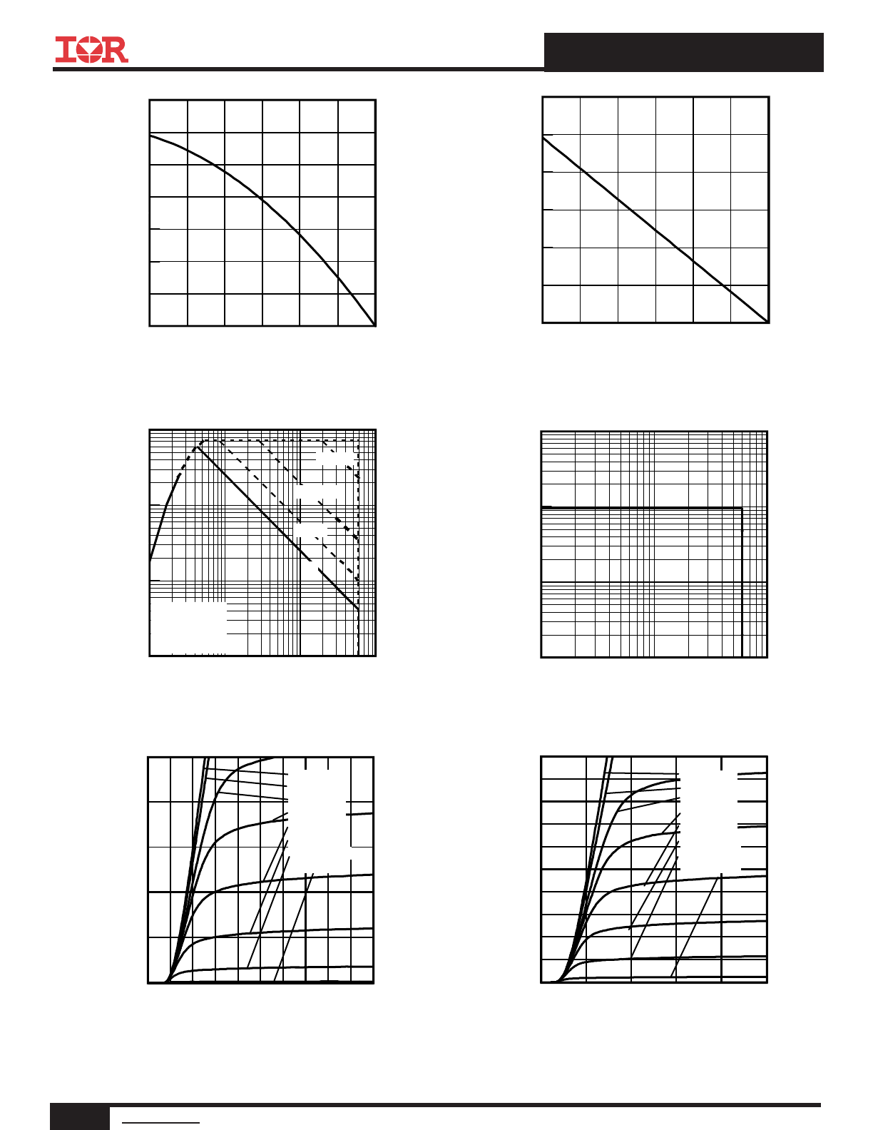
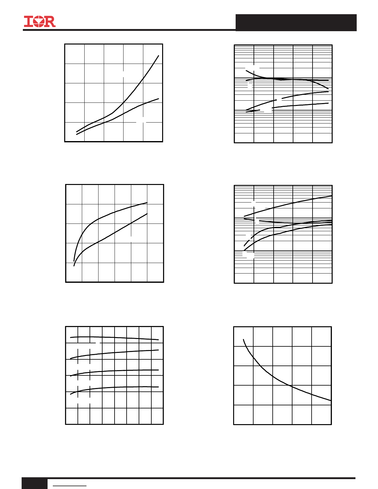
Fig. 1 - Maximum DC Collector Current vs.
Case Temperature
Fig. 2 - Power Dissipation vs. Case
Temperature
Fig. 3 - Forward SOA
T
C
= 25°C, T
J
≤
175°C; V
GE
=15V
Fig. 4 - Reverse Bias SOA
T
J
= 175°C; V
GE
= 20V
Fig. 5 - Typ. IGBT Output Characteristics
T
J
= -40°C; tp = 20μs
Fig. 6 - Typ. IGBT Output Characteristics
T
J
= 25°C; tp = 20μs
25
50
75
100
125
150
175
TC (°C)
0
10
20
30
40
50
60
70
I C
(
A
)
25
50
75
100
125
150
175
TC (°C)
0
50
100
150
200
250
300
P
to
t (
W
)
1
10
100
1000
VCE (V)
0.1
1
10
100
I C
(
A
)
1msec
10μsec
100μsec
Tc = 25°C
Tj = 175°C
Single Pulse
DC
10
100
1000
VCE (V)
1
10
100
1000
I C
(
A
)
0
1
2
3
4
5
6
7
8
9 10
VCE (V)
0
20
40
60
80
100
I C
E
(
A
)
VGE = 18V
VGE = 15V
VGE = 12V
VGE = 11V
VGE = 10V
VGE = 9.0V
VGE = 8.0V
VGE = 7.0V
0
2
4
6
8
10
VCE (V)
0
10
20
30
40
50
60
70
80
90
100
I C
E
(
A
)
VGE = 18V
VGE = 15V
VGE = 12V
VGE = 11V
VGE = 10V
VGE = 9.0V
VGE = 8.0V
VGE = 7.0V
4
www.irf.com
©
2013 International Rectifier
May 02, 2013
AUIRGB/S/SL4062D1
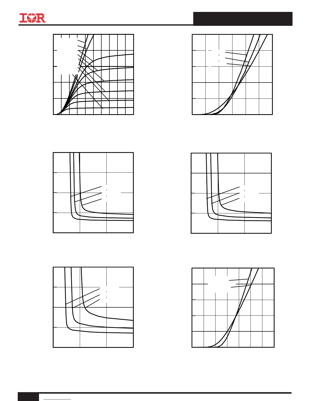
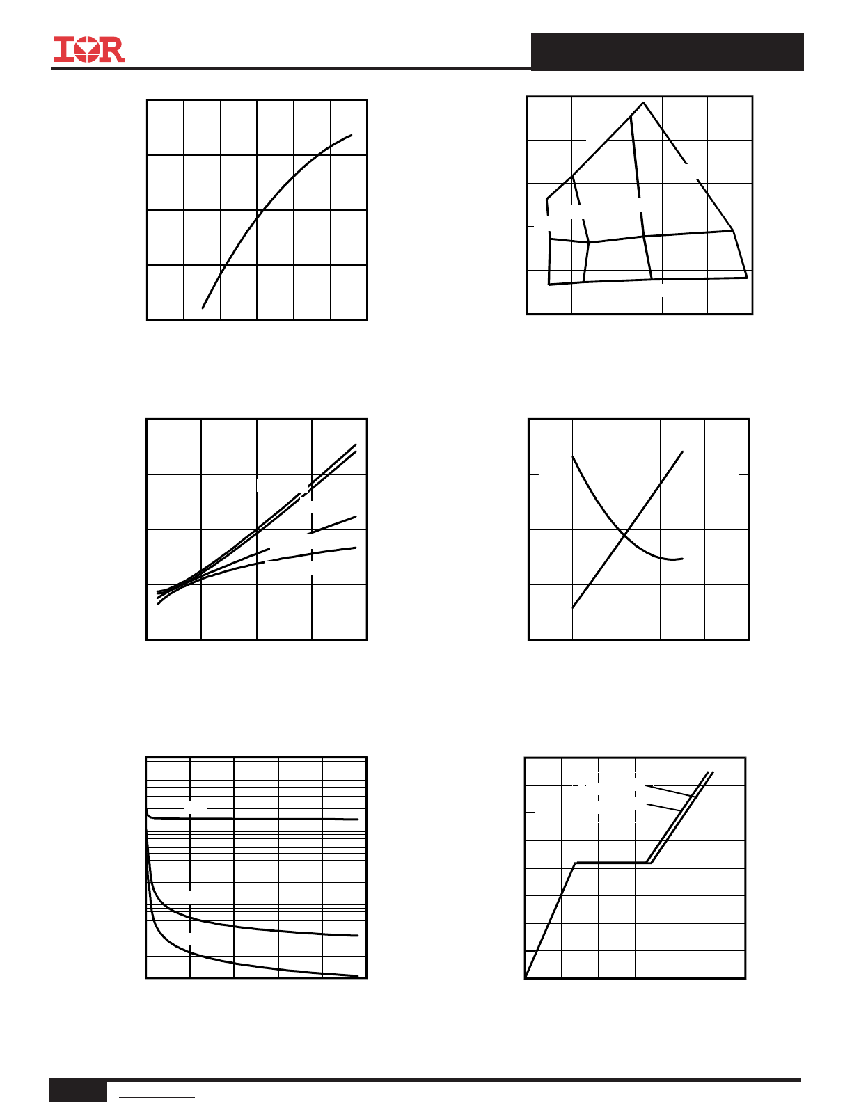
Fig. 7 - Typ. IGBT Output Characteristics
T
J
= 175°C; tp = 20μs
Fig. 8 - Typ. Diode Forward Characteristics
tp = 20μs
Fig. 10 - Typical V
CE
vs. V
GE
T
J
= 25°C
Fig. 11 - Typical V
CE
vs. V
GE
T
J
= 175°C
Fig. 12 - Typ. Transfer Characteristics
V
CE
= 50V; tp = 20μs
Fig. 9 - Typical V
CE
vs. V
GE
T
J
= -40°C
5
10
15
20
VGE (V)
0
2
4
6
8
V
C
E
(
V
)
ICE = 12A
ICE = 24A
ICE = 48A
5
10
15
20
VGE (V)
0
2
4
6
8
V
C
E
(
V
)
ICE = 12A
ICE = 24A
ICE = 48A
5
10
15
20
VGE (V)
0
2
4
6
8
V
C
E
(
V
)
ICE = 12A
ICE = 24A
ICE = 48A
0
1
2
3
4
5
6
7
8
9
10
VCE (V)
0
20
40
60
80
100
I C
E
(
A
)
VGE = 18V
VGE = 15V
VGE = 12V
VGE = 11V
VGE = 10V
VGE = 9.0V
VGE = 8.0V
VGE = 7.0V
0.0
0.5
1.0
1.5
2.0
2.5
3.0
VF (V)
0
20
40
60
80
100
I F
(
A
)
TJ = -40°C
TJ = 25°C
TJ =175°C
2
4
6
8
10
12
14
16
VGE, Gate-to-Emitter Voltage (V)
0
20
40
60
80
100
I C
, C
ol
le
ct
or
-t
o-
E
m
itt
er
C
ur
re
nt
(
A
)
TJ = 25°C
TJ = 175°C
5
www.irf.com
©
2013 International Rectifier
May 02, 2013
AUIRGB/S/SL4062D1
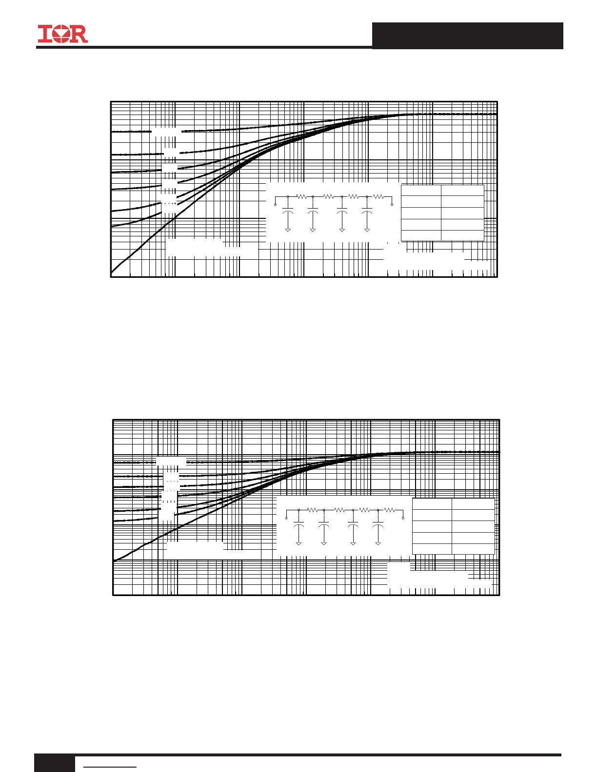
Fig. 13 - Typ. Energy Loss vs. I
C
T
J
= 175°C; L = 210μH; V
CE
= 400V, R
G
= 10
Ω; V
GE
= 15V
Fig. 14 - Typ. Switching Time vs. I
C
T
J
= 175°C; L = 210μH; V
CE
= 400V, R
G
= 10
Ω; V
GE
= 15V
Fig. 15 - Typ. Energy Loss vs. R
G
T
J
= 175°C; L = 210μH; V
CE
= 400V, I
CE
= 24A; V
GE
= 15V
Fig. 16 - Typ. Switching Time vs. R
G
T
J
= 175°C; L = 210μH; V
CE
= 400V, I
CE
= 24A; V
GE
= 15V
Fig. 17 - Typ. Diode I
RR
vs. I
F
T
J
= 175°C
Fig. 18 - Typ. Diode I
RR
vs. R
G
T
J
= 175°C
0
10
20
30
40
50
IC (A)
0
500
1000
1500
2000
2500
E
ne
rg
y
(μ
J)
EOFF
EON
0
10
20
30
40
50
IC (A)
1
10
100
1000
S
w
ic
hi
ng
T
im
e
(n
s)
tR
tdOFF
tF
tdON
0
20
40
60
80
100
120
RG (Ω)
0
400
800
1200
1600
2000
E
ne
rg
y
(μ
J)
EOFF
EON
0
20
40
60
80
100
RG (Ω)
1
10
100
1000
S
w
ic
hi
ng
T
im
e
(n
s)
tR
tdOFF
tF
tdON
10
15
20
25
30
35
40
45
50
IF (A)
5
10
15
20
25
30
35
I R
R
(
A
)
RG = 22Ω
RG = 47Ω
RG = 10Ω
RG = 100Ω
0
20
40
60
80
100
RG (Ω)
10
15
20
25
30
35
I R
R
(
A
)
6
www.irf.com
©
2013 International Rectifier
May 02, 2013
AUIRGB/S/SL4062D1
Fig. 19 - Typ. Diode I
RR
vs. di
F
/dt
V
CC
= 400V; V
GE
= 15V; I
F
= 24A; T
J
= 175°C
Fig. 20 - Typ. Diode Q
RR
vs. di
F
/dt
V
CC
= 400V; V
GE
= 15V; T
J
= 175°C
Fig. 23 - Typ. Capacitance vs. V
CE
V
GE
= 0V; f = 1MHz
Fig. 24 - Typical Gate Charge
vs. V
GE
I
CE
= 24A; L = 585μH
Fig. 21 - Typ. Diode E
RR
vs. I
F
T
J
= 175°C
Fig. 22 - V
GE
vs. Short Circuit Time
V
CC
= 400V; T
C
= 25°C
0
200
400
600
800
1000 1200
diF /dt (A/μs)
15
20
25
30
35
I R
R
(
A
)
200
400
600
800
1000
1200
diF /dt (A/μs)
1000
2000
3000
4000
5000
6000
Q
R
R
(
nC
)
22Ω
10Ω
100Ω
47Ω
12A
48A
24A
10
20
30
40
50
IF (A)
0
500
1000
1500
2000
E
ne
rg
y
(μ
J)
RG = 10Ω
RG = 22Ω
RG = 47Ω
RG = 100Ω
0
100
200
300
400
500
VCE (V)
10
100
1000
10000
C
ap
ac
ita
nc
e
(p
F
)
Cies
Coes
Cres
0
10
20
30
40
50
60
Q G, Total Gate Charge (nC)
0
2
4
6
8
10
12
14
16
V
G
E
, G
at
e-
to
-E
m
itt
er
V
ol
ta
ge
(
V
)
VCES = 400V
VCES = 300V
8
10
12
14
16
18
VGE (V)
0
4
8
12
16
T
im
e
(
μs
)
50
100
150
200
250
C
ur
re
nt
(A
)
Tsc
Isc
7
www.irf.com
©
2013 International Rectifier
May 02, 2013
AUIRGB/S/SL4062D1
Fig. 26. Maximum Transient Thermal Impedance, Junction-to-Case (DIODE)
Fig 25. Maximum Transient Thermal Impedance, Junction-to-Case (IGBT)
1E-006
1E-005
0.0001
0.001
0.01
0.1
1
t1 , Rectangular Pulse Duration (sec)
0.001
0.01
0.1
1
T
he
rm
al
R
es
po
ns
e
(
Z
th
JC
)
0.20
0.10
D = 0.50
0.02
0.01
0.05
SINGLE PULSE
( THERMAL RESPONSE )
Notes:
1. Duty Factor D = t1/t2
2. Peak Tj = P dm x Zthjc + Tc
τ
J
τ
J
τ
1
τ
1
τ
2
τ
2
τ
3
τ
3
R
1
R
1
R
2
R
2
R
3
R
3
Ci i
/Ri
Ci=
τi/Ri
τ
τ
C
τ
4
τ
4
R
4
R
4
Ri (°C/W)
τi (sec)
0.0347 0.00003
0.1519 0.00007
0.2531 0.00209
0.1721 0.01166
1E-006
1E-005
0.0001
0.001
0.01
0.1
1
t1 , Rectangular Pulse Duration (sec)
0.0001
0.001
0.01
0.1
1
10
T
he
rm
al
R
es
po
ns
e
(
Z
th
JC
)
0.20
0.10
D = 0.50
0.02
0.01
0.05
SINGLE PULSE
( THERMAL RESPONSE )
Notes:
1. Duty Factor D = t1/t2
2. Peak Tj = P dm x Zthjc + Tc
τ
J
τ
J
τ
1
τ
1
τ
2
τ
2
τ
3
τ
3
R
1
R
1
R
2
R
2
R
3
R
3
Ci i
/Ri
Ci=
τi/Ri
τ
τ
C
τ
4
τ
4
R
4
R
4
Ri (°C/W)
τi (sec)
0.0296 0.00003
0.4307 0.00028
0.4840 0.00353
0.2576 0.01971
8
www.irf.com
©
2013 International Rectifier
May 02, 2013
AUIRGB/S/SL4062D1
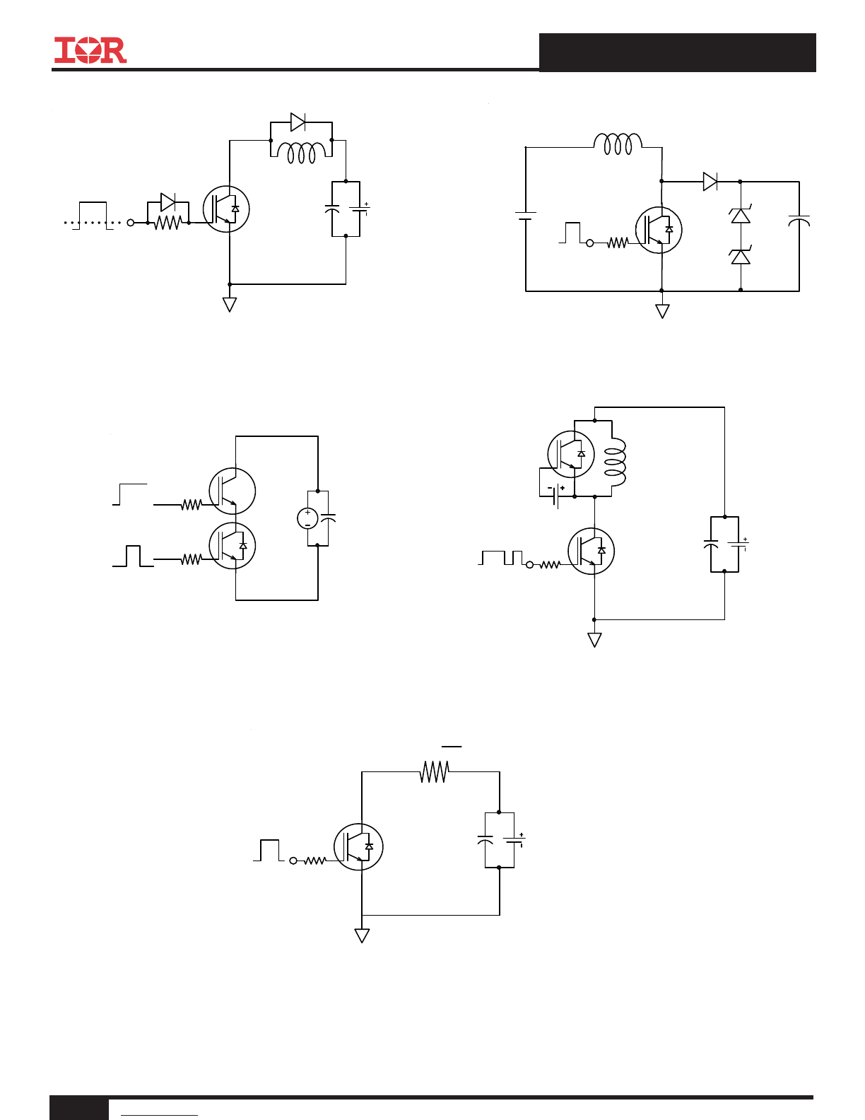
Fig.C.T.1 - Gate Charge Circuit (turn-off)
Fig.C.T.2 - RBSOA Circuit
0
1K
VCC
DUT
L
L
Rg
80 V
DUT
VCC
+
-
Fig.C.T.5 - Resistive Load Circuit
Rg
VCC
DUT
R =
VCC
ICM
Fig.C.T.3 - S.C. SOA Circuit
DC
4X
DUT
VCC
SCSOA
Fig.C.T.4 - Switching Loss Circuit
L
Rg
VCC
DUT /
DRIVER
diode clamp /
DUT
-5V
9
www.irf.com
©
2013 International Rectifier
May 02, 2013
AUIRGB/S/SL4062D1
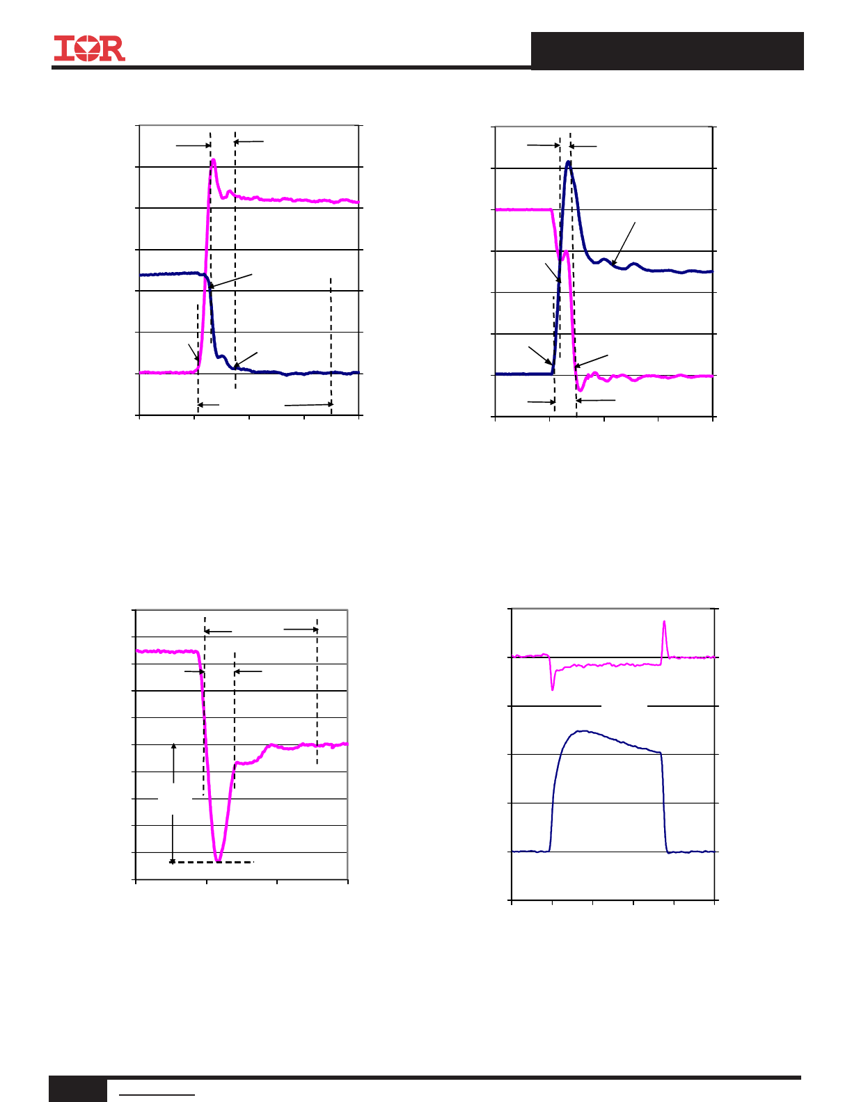
Fig. WF3 - Typ. Diode Recovery Waveform
@ T
J
= 175°C using Fig. CT.4
Fig. WF1 - Typ. Turn-off Loss Waveform
@ T
J
= 175°C using Fig. CT.4
Fig. WF2 - Typ. Turn-on Loss Waveform
@ T
J
= 175°C using Fig. CT.4
Fig. WF4 - Typ. S.C. Waveform
@ T
J
= 25°C using Fig. CT.3
-10
0
10
20
30
40
50
60
-100
0
100
200
300
400
500
600
-0.3
-0.05
0.2
0.45
0.7
I
CE
(A)
V
CE
(V)
time(μs)
90% I
CE
5% V
CE
10% I
CE
Eoff Loss
tf
-10
0
10
20
30
40
50
60
-100
0
100
200
300
400
500
600
-0.3
-0.05
0.2
0.45
0.7
I
CE
(A
)
V
CE
(V
)
time (μs)
TEST
CURRENT
90%
/
5% V
CE
10%
/
tr
Eon Loss
-35
-28
-21
-14
-7
0
7
14
21
28
35
-0.25
0.00
0.25
0.50
I
F
(A
)
time (μS)
Peak
I
RR
t
RR
Q
RR
-100
0
100
200
300
400
500
-100
0
100
200
300
400
500
-2
0
2
4
6
8
Ic
e (
A
)
Vce
(V)
Time (uS)
VCE
ICE
10
www.irf.com
©
2013 International Rectifier
May 02, 2013
AUIRGB/S/SL4062D1
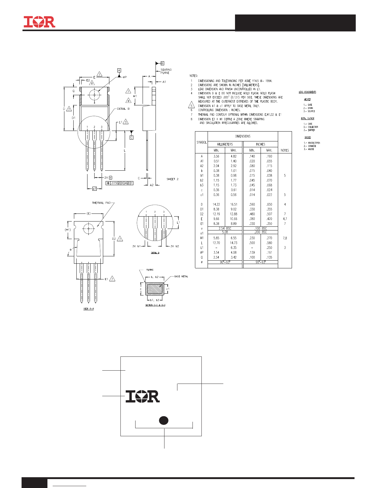
TO-220AB Part Marking Information
TO-220AB Package Outline
Dimensions are shown in millimeters (inches)
Note: For the most current drawing please refer to IR website at http://www.irf.com/package/
Lot Code
YWWA
XX or XX
Part Number
IR Logo
AUGB4062D1
Date Code
Y= Year
WW= Work Week
A= Automotive, Lead Free