
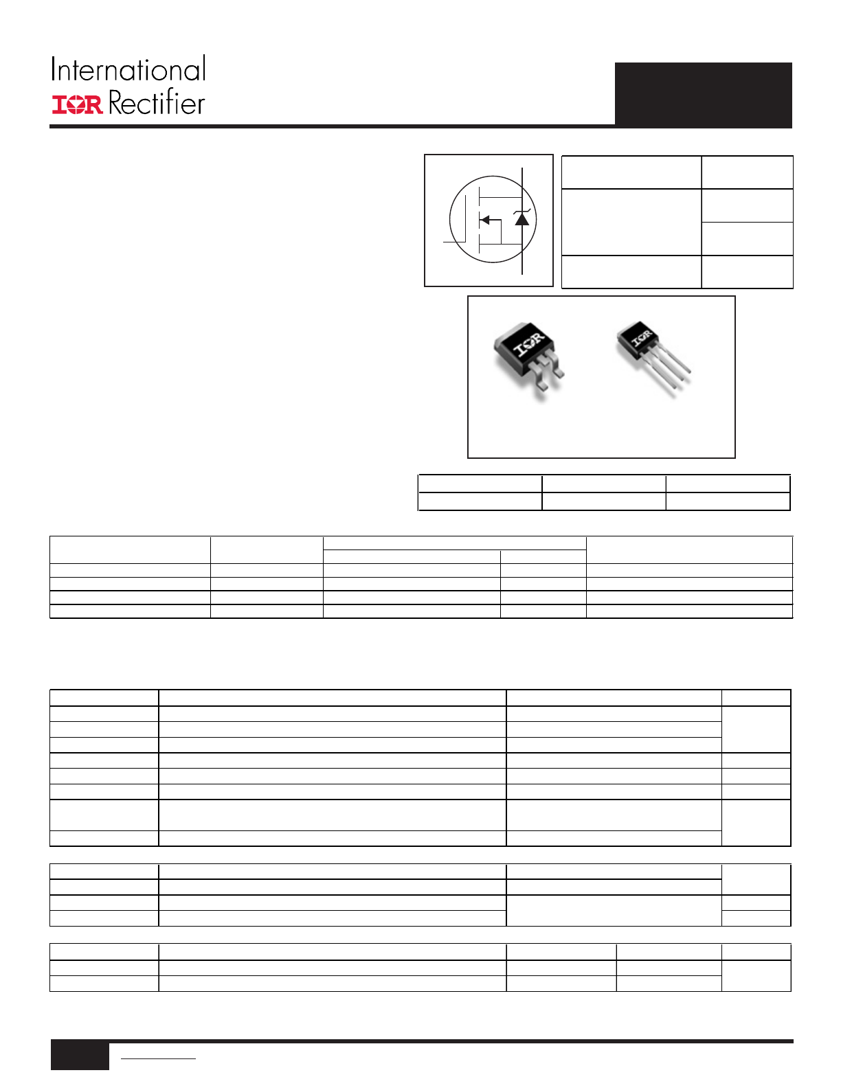
HEXFET
®
Power MOSFET
S
D
G
AUTOMOTIVE GRADE
Absolute Maximum Ratings
Stresses beyond those listed under “Absolute Maximum Ratings” may cause permanent damage to the device. These are stress ratings only; and
functional operation of the device at these or any other condition beyond those indicated in the specifications is not implied. Exposure to absolute-
maximum-rated conditions for extended periods may affect device reliability. The thermal resistance and power dissipation ratings are measured under
board mounted and still air conditions. Ambient temperature (T
A
) is 25°C, unless otherwise specified.
G
D
S
Gate
Drain
Source
HEXFET
®
is a registered trademark of International Rectifier.
*Qualification standards can be found at http://www.irf.com/
Description
Specifically designed for Automotive applications, this HEXFET®
Power MOSFET utilizes the latest processing techniques to achieve
extremely low on-resistance per silicon area. Additional features
of this design are a 175°C junction operating temperature, fast
switching speed and improved repetitive avalanche rating. These
features combine to make this design an extremely efficient and
reliable device for use in Automotive applications and wide variety
of other applications.
Features
l
Advanced Process Technology
l
New Ultra Low On-Resistance
l
175°C Operating Temperature
l
Fast Switching
l
Repetitive Avalanche Allowed up to Tjmax
l
Lead-Free, RoHS Compliant
l
Automotive Qualified *
Applications
l
Electric Power Steering (EPS)
l
Battery Switch
l
Start/Stop Micro Hybrid
l
Heavy Loads
l
DC-DC Converter
D
2
Pak
AUIRFS8403
TO-262
AUIRFSL8403
S
D
G
D
D
S
G
AUIRFS8403
AUIRFSL8403
Ordering Information
Base part number
Package Type
Standard Pack
Complete Part Number
Form
Quantity
AUIRFSL8403
TO-262
Tube
50
AUIRFSL8403
AUIRFS8403
D2Pak
Tube
50
AUIRFS8403
Tape and Reel Left
800
AUIRFS8403TRL
Tape and Reel Right
800
AUIRFS8403TRR
V
DSS
40V
R
DS(on)
typ.
2.6m
Ω
max.
3.3m
Ω
I
D (Silicon Limited)
123A
Symbol
Parameter
Units
I
D
@ T
C
= 25°C
Continuous Drain Current, V
GS
@ 10V (Silicon Limited)
I
D
@ T
C
= 100°C
Continuous Drain Current, V
GS
@ 10V (Silicon Limited)
I
DM
Pulsed Drain Current
c
P
D
@T
C
= 25°C
Maximum Power Dissipation
W
Linear Derating Factor
W/°C
V
GS
Gate-to-Source Voltage
V
T
J
Operating Junction and
T
STG
Storage Temperature Range
Soldering Temperature, for 10 seconds (1.6mm from case)
Avalanche Characteristics
E
AS (Thermally limited)
Single Pulse Avalanche Energy
d
E
AS
(tested)
Single Pulse Avalanche Energy Tested Value
j
I
AR
Avalanche Current
c
A
E
AR
Repetitive Avalanche Energy
c
mJ
Thermal Resistance
Symbol
Parameter
Typ.
Max.
Units
R
θJC
Junction-to-Case
i
–––
1.52
R
θJA
Junction-to-Ambient (PCB Mount) D2 Pak
–––
40
°C/W
Max.
123
87
492
160
-55 to + 175
± 20
0.66
See Fig. 14, 15 , 24a, 24b
A
°C
300
111
99
mJ
1
www.irf.com
©
2013 International Rectifier
May 08 2013
AUIRFS/SL8403
2
www.irf.com
©
2013 International Rectifier
May 08 2013
S
D
G
Notes:
Repetitive rating; pulse width limited by max. junction temperature.
Limited by T
Jmax
, starting T
J
= 25°C, L = 0.046mH,R
G
= 50
Ω,
I
AS
= 70A, V
GS
=10V.
I
SD
≤ 70A, di/dt ≤ 1174A/μs, V
DD
≤ V
(BR)DSS
, T
J
≤ 175°C.
Pulse width
≤ 400μs; duty cycle ≤ 2%.
C
oss
eff. (TR) is a fixed capacitance that gives the same charging
time as C
oss
while V
DS
is rising from 0 to 80% V
DSS
.
C
oss
eff. (ER) is a fixed capacitance that gives the same energy as
C
oss
while V
DS
is rising from 0 to 80% V
DSS
.
R
θ
is measured at T
J
approximately 90°C.
This value determined from sample failure population,
starting T
J
= 25°C, L=0.046mH, R
G
= 50
Ω, I
AS
= 70A, V
GS
=10V.
Static @ T
J
= 25°C (unless otherwise specified)
Symbol
Parameter
Min.
Typ. Max. Units
V
(BR)DSS
Drain-to-Source Breakdown Voltage
40
–––
–––
V
ΔV
(BR)DSS
/
ΔT
J
Breakdown Voltage Temp. Coefficient
–––
0.033
–––
V/°C
R
DS(on)
Static Drain-to-Source On-Resistance
–––
2.6
3.3
m
Ω
V
GS(th)
Gate Threshold Voltage
2.2
3.0
3.9
V
I
DSS
Drain-to-Source Leakage Current
–––
–––
1.0
–––
–––
150
I
GSS
Gate-to-Source Forward Leakage
–––
–––
100
Gate-to-Source Reverse Leakage
–––
–––
-100
R
G
Internal Gate Resistance
–––
1.6
–––
Ω
Dynamic @ T
J
= 25°C (unless otherwise specified)
Symbol
Parameter
Min.
Typ. Max. Units
gfs
Forward Transconductance
269
–––
–––
S
Q
g
Total Gate Charge
–––
62
93
Q
gs
Gate-to-Source Charge
–––
16
–––
Q
gd
Gate-to-Drain ("Miller") Charge
–––
20
–––
Q
sync
Total Gate Charge Sync. (Q
g
- Q
gd
)
–––
42
–––
t
d(on)
Turn-On Delay Time
–––
10
–––
t
r
Rise Time
–––
77
–––
t
d(off)
Turn-Off Delay Time
–––
26
–––
t
f
Fall Time
–––
43
–––
C
iss
Input Capacitance
–––
3183
–––
C
oss
Output Capacitance
–––
475
–––
C
rss
Reverse Transfer Capacitance
–––
331
–––
C
oss
eff. (ER)
Effective Output Capacitance (Energy Related)
–––
596
–––
C
oss
eff. (TR)
Effective Output Capacitance (Time Related)
–––
688
–––
Diode Characteristics
Symbol
Parameter
Min.
Typ. Max. Units
I
S
Continuous Source Current
(Body Diode)
I
SM
Pulsed Source Current
(Body Diode)
c
V
SD
Diode Forward Voltage
–––
0.9
1.3
V
dv/dt
Peak Diode Recovery
e
–––
7.6
–––
V/ns
t
rr
Reverse Recovery Time
–––
22
–––
T
J
= 25°C
V
R
= 34V,
–––
24
–––
T
J
= 125°C
I
F
= 70A
Q
rr
Reverse Recovery Charge
–––
15
–––
T
J
= 25°C
di/dt = 100A/μs
f
–––
15
–––
T
J
= 125°C
I
RRM
Reverse Recovery Current
–––
1.0
–––
A
T
J
= 25°C
nC
472
integral reverse
p-n junction diode.
T
J
= 25°C, I
S
= 70A, V
GS
= 0V
f
T
J
= 175°C, I
S
= 70A, V
DS
= 40V
ns
V
GS
= 0V, V
DS
= 0V to 32V
g
Conditions
–––
–––
118
A
MOSFET symbol
showing the
–––
–––
ns
V
DD
= 26V
I
D
= 70A
R
G
=1
Ω
V
GS
= 10V
f
pF
V
GS
= 0V
V
DS
= 25V
ƒ = 1.0 MHz, See Fig. 5
V
GS
= 0V, V
DS
= 0V to 32V
h, See Fig. 11
Conditions
V
DS
= 10V, I
D
= 70A
nC
I
D
= 70A
V
DS
=20V
V
GS
= 10V
f
I
D
= 70A, V
DS
=0V, V
GS
= 10V
Conditions
V
GS
= 0V, I
D
= 250μA
Reference to 25°C, I
D
= 5mA
c
V
GS
= 10V, I
D
= 70A
f
V
DS
= V
GS
, I
D
= 100μA
μA
nA
V
DS
= 40V, V
GS
= 0V
V
DS
= 40V, V
GS
= 0V, T
J
= 125°C
V
GS
= 20V
V
GS
= -20V
AUIRFS/SL8403
3
www.irf.com
©
2013 International Rectifier
May 08 2013
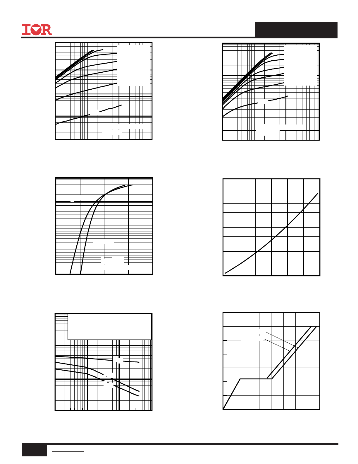
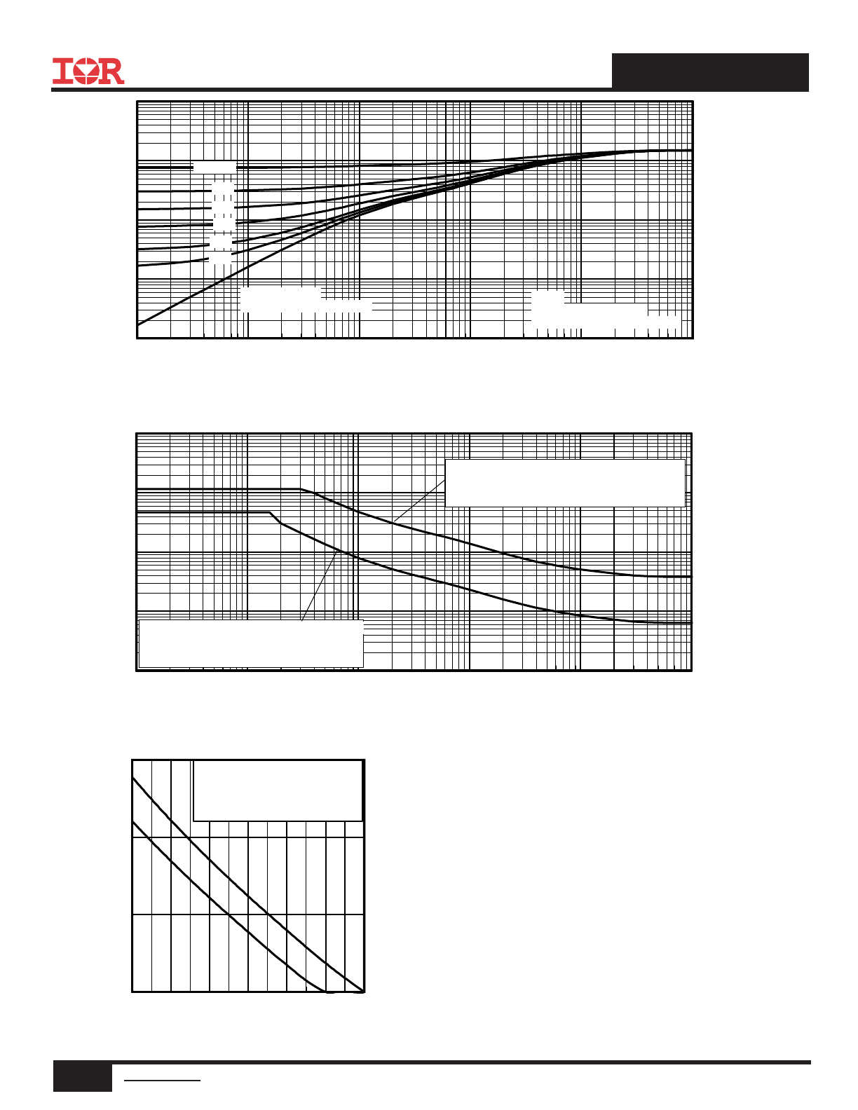
Fig 1. Typical Output Characteristics
Fig 3. Typical Transfer Characteristics
Fig 4. Normalized On-Resistance vs. Temperature
Fig 2. Typical Output Characteristics
Fig 6. Typical Gate Charge vs. Gate-to-Source Voltage
Fig 5. Typical Capacitance vs. Drain-to-Source Voltage
0.1
1
10
100
VDS, Drain-to-Source Voltage (V)
0.1
1
10
100
1000
I D
, D
ra
in
-t
o-
S
ou
rc
e
C
ur
re
nt
(
A
)
VGS
TOP
15V
10V
8.0V
7.0V
6.0V
5.5V
5.0V
BOTTOM
4.5V
≤60μs
PULSE WIDTH
Tj = 25°C
4.5V
0.1
1
10
100
VDS, Drain-to-Source Voltage (V)
1
10
100
1000
I D
, D
ra
in
-t
o-
S
ou
rc
e
C
ur
re
nt
(
A
)
4.5V
≤60μs
PULSE WIDTH
Tj = 175°C
VGS
TOP
15V
10V
8.0V
7.0V
6.0V
5.5V
5.0V
BOTTOM
4.5V
2
4
6
8
10
VGS, Gate-to-Source Voltage (V)
0.1
1
10
100
1000
I D
, D
ra
in
-t
o-
S
ou
rc
e
C
ur
re
nt
(
A
)
TJ = 25°C
TJ = 175°C
VDS = 10V
≤60μs PULSE WIDTH
-60
-20
20
60
100
140
180
TJ , Junction Temperature (°C)
0.6
1.0
1.4
1.8
2.2
R
D
S
(o
n)
,
D
ra
in
-t
o-
S
ou
rc
e
O
n
R
es
is
ta
nc
e
(
N
or
m
al
iz
ed
)
ID = 70A
VGS = 10V
0.1
1
10
100
VDS, Drain-to-Source Voltage (V)
100
1000
10000
100000
C
, C
ap
ac
ita
nc
e
(p
F
)
VGS = 0V, f = 1 MHZ
Ciss = Cgs + Cgd, C ds SHORTED
Crss = Cgd
Coss = Cds + Cgd
Coss
Crss
Ciss
0
10
20
30
40
50
60
70
80
QG, Total Gate Charge (nC)
0.0
2.0
4.0
6.0
8.0
10.0
12.0
14.0
V
G
S
, G
at
e-
to
-S
ou
rc
e
V
ol
ta
ge
(
V
)
VDS= 32V
VDS= 20V
ID= 70A
AUIRFS/SL8403
4
www.irf.com
©
2013 International Rectifier
May 08 2013
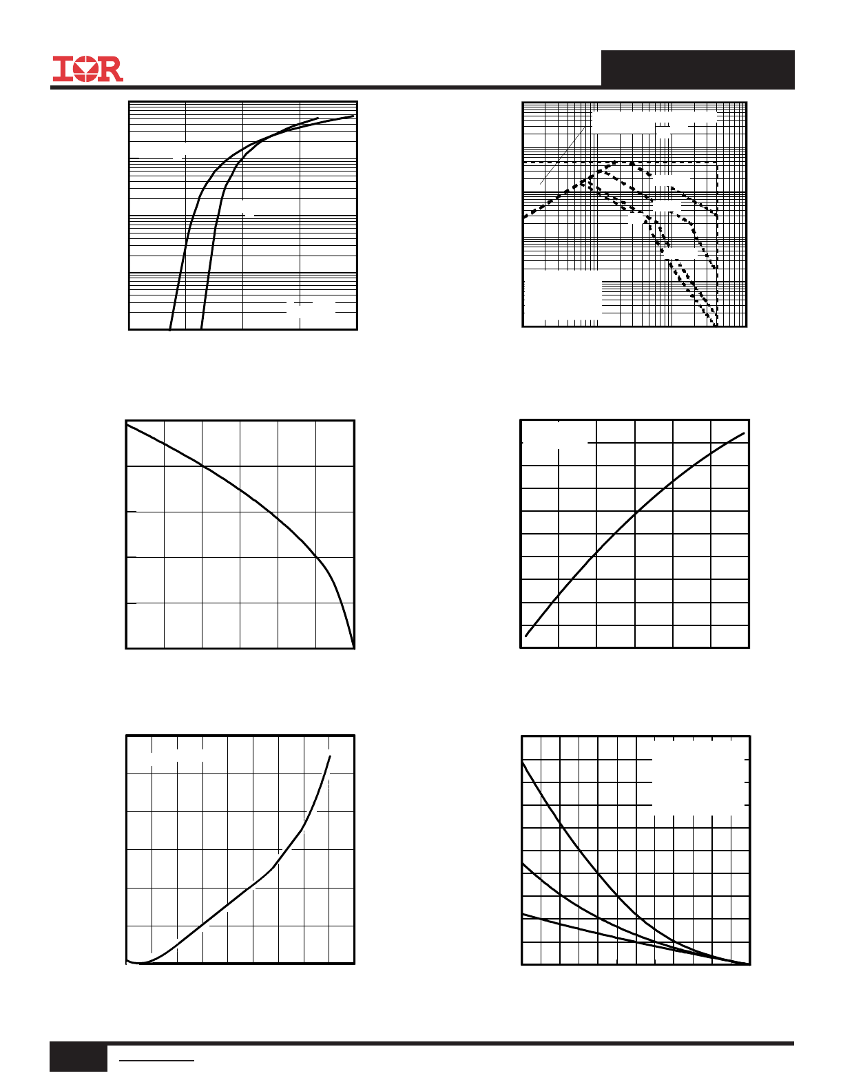
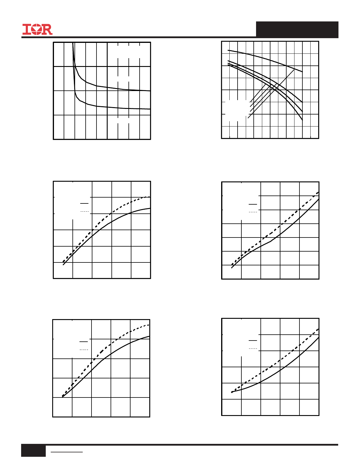
Fig 8. Maximum Safe Operating Area
Fig 10. Drain-to-Source Breakdown Voltage
Fig 7. Typical Source-Drain Diode
Forward Voltage
Fig 11. Typical C
OSS
Stored Energy
Fig 9. Maximum Drain Current vs.
Case Temperature
Fig 12. Maximum Avalanche Energy vs. DrainCurrent
0.0
0.5
1.0
1.5
2.0
VSD, Source-to-Drain Voltage (V)
0.1
1
10
100
1000
I S
D
, R
ev
er
se
D
ra
in
C
ur
re
nt
(
A
)
TJ = 25°C
TJ = 175°C
VGS = 0V
0.1
1
10
100
VDS, Drain-to-Source Voltage (V)
0.1
1
10
100
1000
10000
I D
,
D
ra
in
-t
o-
S
ou
rc
e
C
ur
re
nt
(
A
)
Tc = 25°C
Tj = 175°C
Single Pulse
10msec
1msec
OPERATION IN THIS AREA
LIMITED BY R DS(on)
100μsec
DC
-60
-20
20
60
100
140
180
TJ , Temperature ( °C )
40
41
42
43
44
45
46
47
48
49
50
V
(B
R
)D
S
S
, D
ra
in
-t
o-
S
ou
rc
e
B
re
ak
do
w
n
V
ol
ta
ge
(
V
)
Id = 5.0mA
0
5
10
15
20
25
30
35
40
45
VDS, Drain-to-Source Voltage (V)
0.0
0.1
0.2
0.3
0.4
0.5
0.6
E
ne
rg
y
(μ
J)
VDS= 0V to 32V
25
50
75
100
125
150
175
TC , Case Temperature (°C)
0
25
50
75
100
125
I D
,
D
ra
in
C
ur
re
nt
(
A
)
25
50
75
100
125
150
175
Starting TJ , Junction Temperature (°C)
0
50
100
150
200
250
300
350
400
450
500
E
A
S
,
S
in
gl
e
P
ul
se
A
va
la
nc
he
E
ne
rg
y
(m
J)
ID
TOP 12A
23A
BOTTOM 70A
AUIRFS/SL8403
5
www.irf.com
©
2013 International Rectifier
May 08 2013
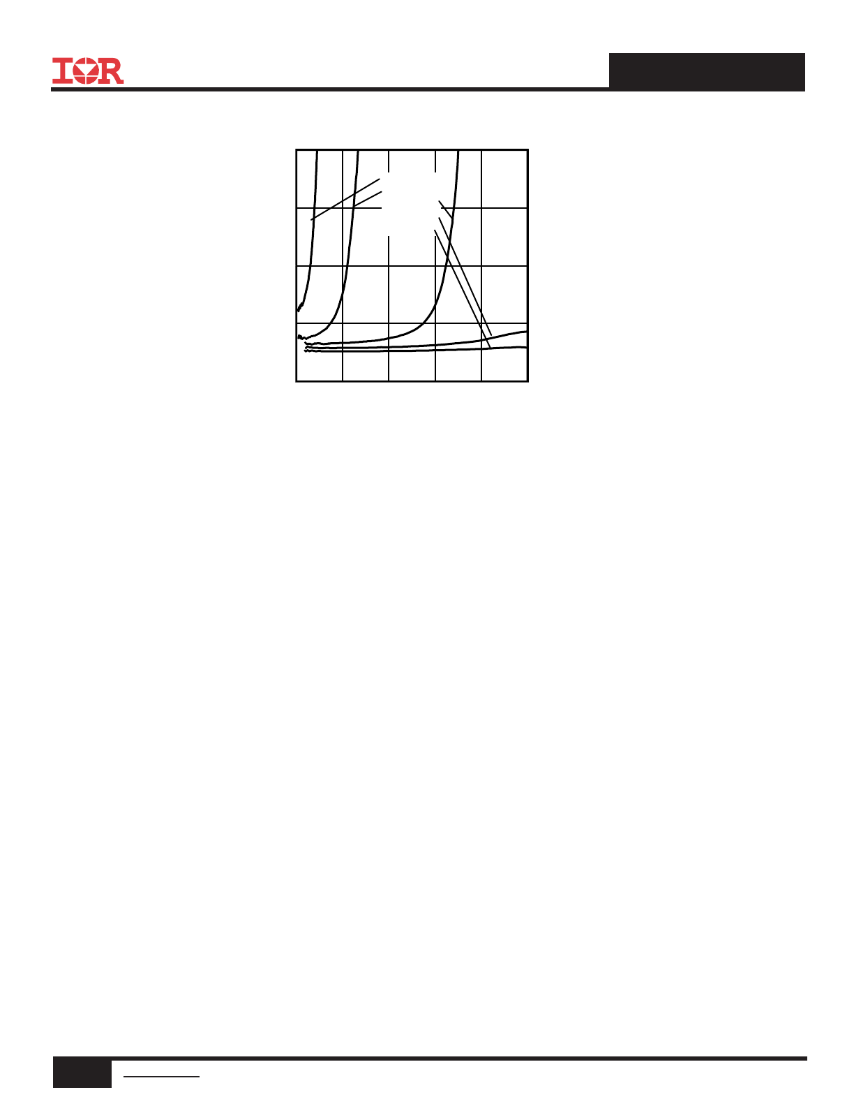
Fig 13. Maximum Effective Transient Thermal Impedance, Junction-to-Case
Fig 14. Typical Avalanche Current vs.Pulsewidth
Fig 15. Maximum Avalanche Energy vs. Temperature
Notes on Repetitive Avalanche Curves , Figures 14, 15
(For further info, see AN-1005 at www.irf.com)
1. Avalanche failures assumption:
Purely a thermal phenomenon and failure occurs at a temperature far in
excess of T
jmax
. This is validated for every part type.
2. Safe operation in Avalanche is allowed as long asT
jmax
is not exceeded.
3. Equation below based on circuit and waveforms shown in Figures 24a, 24b.
4. P
D (ave)
= Average power dissipation per single avalanche pulse.
5. BV = Rated breakdown voltage (1.3 factor accounts for voltage increase
during avalanche).
6. I
av
= Allowable avalanche current.
7.
ΔT
=
Allowable rise in junction temperature, not to exceed
T
jmax
(assumed as
25°C in Figure 14, 15).
t
av =
Average time in avalanche.
D = Duty cycle in avalanche = t
av
·f
Z
thJC
(D, t
av
) = Transient thermal resistance, see Figures 13)
P
D (ave)
= 1/2 ( 1.3·BV·I
av
) =
DT/ Z
thJC
I
av
=
2
DT/ [1.3·BV·Z
th
]
E
AS (AR)
= P
D (ave)
·t
av
1E-006
1E-005
0.0001
0.001
0.01
0.1
t1 , Rectangular Pulse Duration (sec)
0.001
0.01
0.1
1
10
T
he
rm
al
R
es
po
ns
e
(
Z
th
JC
)
°
C
/W
0.20
0.10
D = 0.50
0.02
0.01
0.05
SINGLE PULSE
( THERMAL RESPONSE )
Notes:
1. Duty Factor D = t1/t2
2. Peak Tj = P dm x Zthjc + Tc
1.0E-06
1.0E-05
1.0E-04
1.0E-03
1.0E-02
1.0E-01
tav (sec)
0.1
1
10
100
1000
A
va
la
nc
he
C
ur
re
nt
(
A
)
Allowed avalanche Current vs avalanche
pulsewidth, tav, assuming
ΔΤj = 25°C and
Tstart = 150°C.
Allowed avalanche Current vs avalanche
pulsewidth, tav, assuming
ΔTj = 150°C and
Tstart = 25°C (Single Pulse)
25
50
75
100
125
150
175
Starting TJ , Junction Temperature (°C)
0
40
80
120
E
A
R
,
A
va
la
nc
he
E
ne
rg
y
(m
J)
TOP Single Pulse
BOTTOM 1.0% Duty Cycle
ID = 70A
AUIRFS/SL8403
6
www.irf.com
©
2013 International Rectifier
May 08 2013
Fig. 18 - Typical Recovery Current vs. di
f
/dt
Fig 17. Threshold Voltage vs. Temperature
Fig. 19 - Typical Stored Charge vs. di
f
/dt
Fig. 20 - Typical Recovery Current vs. di
f
/dt
Fig. 21 - Typical Stored Charge vs. di
f
/dt
Fig 16. On-Resistance vs. Gate Voltage
2
4
6
8
10
12
14
16
18
20
VGS, Gate -to -Source Voltage (V)
0
2
4
6
8
R
D
S
(o
n)
,
D
ra
in
-t
o
-S
ou
rc
e
O
n
R
es
is
ta
nc
e
(m
Ω
)
ID = 70A
TJ = 25°C
TJ = 125°C
-75
-25
25
75
125
175
225
TJ , Temperature ( °C )
0.5
1.5
2.5
3.5
4.5
V
G
S
(t
h)
, G
at
e
th
re
sh
ol
d
V
ol
ta
ge
(
V
)
ID = 100μA
ID = 250μA
ID = 1.0mA
ID = 1.0A
0
200
400
600
800
1000
diF /dt (A/μs)
0
1
2
3
4
5
6
I R
R
M
(
A
)
IF = 46A
VR = 34V
TJ = 25°C
TJ = 125°C
0
200
400
600
800
1000
diF /dt (A/μs)
0
10
20
30
40
50
60
70
Q
R
R
(
nC
)
IF = 46A
VR = 34V
TJ = 25°C
TJ = 125°C
0
200
400
600
800
1000
diF /dt (A/μs)
0
1
2
3
4
5
I R
R
M
(
A
)
IF = 70A
VR = 34V
TJ = 25°C
TJ = 125°C
0
200
400
600
800
1000
diF /dt (A/μs)
0
10
20
30
40
50
60
Q
R
R
(
nC
)
IF = 70A
VR = 34V
TJ = 25°C
TJ = 125°C
AUIRFS/SL8403
7
www.irf.com
©
2013 International Rectifier
May 08 2013
Fig 22. Typical On-Resistance vs. Drain Current
0
100
200
300
400
500
ID, Drain Current (A)
0.0
5.0
10.0
15.0
20.0
R
D
S
(o
n)
,
D
ra
in
-t
o
-S
ou
rc
e
O
n
R
es
is
ta
nc
e
(m
Ω
)
VGS = 5.5V
VGS = 6.0V
VGS = 7.0V
VGS = 8.0V
VGS = 10V
AUIRFS/SL8403
8
www.irf.com
©
2013 International Rectifier
May 08 2013
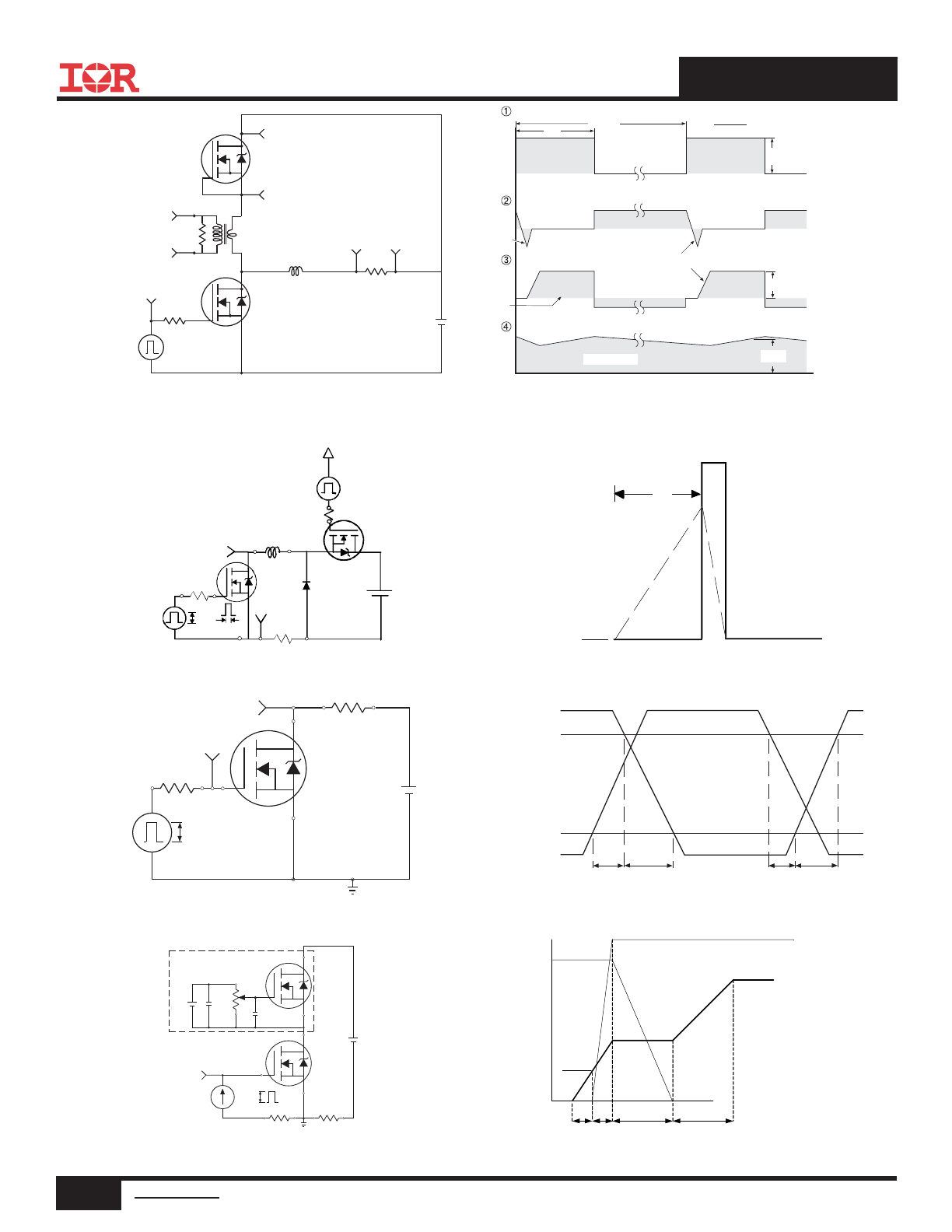
Fig 25a. Switching Time Test Circuit
Fig 25b. Switching Time Waveforms
Fig 24b. Unclamped Inductive Waveforms
Fig 24a. Unclamped Inductive Test Circuit
tp
V
(BR)DSS
I
AS
RG
IAS
0.01
Ω
tp
D.U.T
L
VDS
+
- VDD
DRIVER
A
15V
20V
V
GS
Fig 26a. Gate Charge Test Circuit
Fig 26b. Gate Charge Waveform
Vds
Vgs
Id
Vgs(th)
Qgs1 Qgs2
Qgd
Qgodr
Fig 23.
Peak Diode Recovery dv/dt Test Circuit for N-Channel
HEXFET
®
Power MOSFETs
Circuit Layout Considerations
• Low Stray Inductance
• Ground Plane
• Low Leakage Inductance
Current Transformer
P.W.
Period
di/dt
Diode Recovery
dv/dt
Ripple
≤ 5%
Body Diode Forward Drop
Re-Applied
Voltage
Reverse
Recovery
Current
Body Diode Forward
Current
V
GS
=10V
V
DD
I
SD
Driver Gate Drive
D.U.T. I
SD
Waveform
D.U.T. V
DS
Waveform
Inductor Curent
D =
P.W.
Period
*
V
GS
= 5V for Logic Level Devices
*
+
-
+
+
+
-
-
-
R
G
V
DD
• dv/dt controlled by R
G
• Driver same type as D.U.T.
• I
SD
controlled by Duty Factor "D"
• D.U.T. - Device Under Test
D.U.T
Inductor Current
D.U.T.
V
DS
I
D
I
G
3mA
V
GS
.3
μF
50K
Ω
.2
μF
12V
Current Regulator
Same Type as D.U.T.
Current Sampling Resistors
+
-
V
DS
90%
10%
V
GS
t
d(on)
t
r
t
d(off)
t
f
V
DS
Pulse Width ≤ 1 µs
Duty Factor ≤ 0.1 %
R
D
V
GS
R
G
D.U.T.
10V
+
-
V
DD
V
GS
AUIRFS/SL8403
9
www.irf.com
©
2013 International Rectifier
May 08 2013
D
2
Pak Part Marking Information
D
2
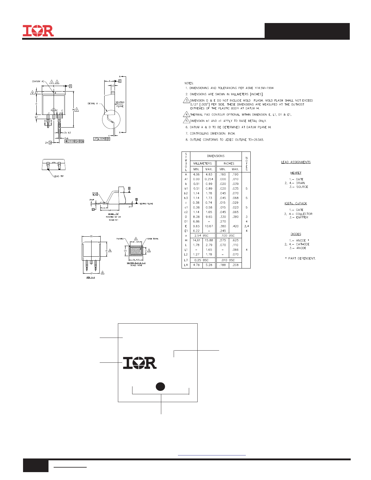
Pak Package Outline (
Dimensions are shown in millimeters (inches))
Note: For the most current drawing please refer to IR website at
http://www.irf.com/package/
Lot Code
YWWA
XX or XX
Part Number
IR Logo
AUIRFS8403
Date Code
Y= Year
WW= Work Week
A= Automotive, Lead Free
AUIRFS/SL8403
10
www.irf.com
©
2013 International Rectifier
May 08 2013
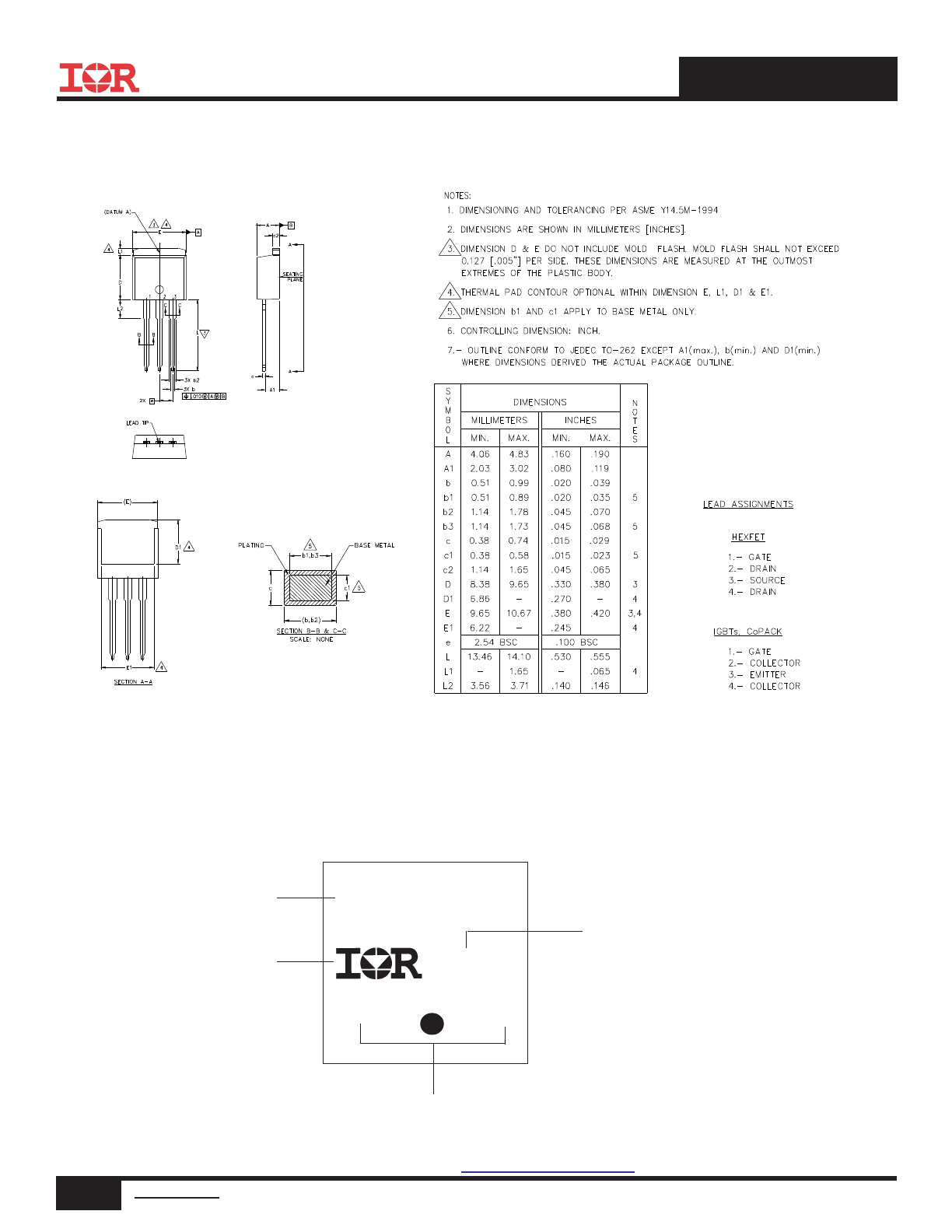
TO-262 Part Marking Information
TO-262 Package Outline (
Dimensions are shown in millimeters (inches))
Note: For the most current drawing please refer to IR website at
http://www.irf.com/package/
Lot Code
YWWA
XX or XX
Part Number
IR Logo
AUIRFSL8403
Date Code
Y= Year
WW= Work Week
A= Automotive, Lead Free