
AUIRFR4104
AUIRFU4104
V
DSS
40V
R
DS(on)
max.
5.5m
I
D (Silicon Limited)
119A
I
D (Package Limited)
42A
Features
Advanced Process Technology
Low
On-Resistance
175°C Operating Temperature
Fast Switching
Repetitive Avalanche Allowed up to Tjmax
Lead-Free, RoHS Compliant
Automotive Qualified *
Description
Specifically designed for Automotive applications, this HEXFET®
Power MOSFET utilizes the latest processing techniques to
achieve extremely low on-resistance per silicon area. Additional
features of this design are a 175°C junction operating temperature,
fast switching speed and improved repetitive avalanche rating .
These features combine to make this design an extremely efficient
and reliable device for use in Automotive applications and a wide
variety of other applications.
1
2015-12-1
HEXFET® is a registered trademark of Infineon.
*Qualification standards can be found at
www.infineon.com
AUTOMOTIVE GRADE
Symbol Parameter
Max.
Units
I
D
@ T
C
= 25°C
Continuous Drain Current, V
GS
@ 10V (Silicon Limited)
119
A
I
D
@ T
C
= 100°C
Continuous Drain Current, V
GS
@ 10V (Silicon Limited)
84
I
DM
Pulsed Drain Current 480
P
D
@T
C
= 25°C
Maximum Power Dissipation
140
W
Linear Derating Factor
0.95
W/°C
V
GS
Gate-to-Source Voltage
± 20
V
E
AS
Single Pulse Avalanche Energy (Thermally Limited) 145
E
AS
(Tested)
Single Pulse Avalanche Energy Tested Value 310
I
AR
Avalanche Current
See Fig.15,16, 12a, 12b
A
E
AR
Repetitive Avalanche Energy
mJ
T
J
Operating Junction and
-55 to + 175
T
STG
Storage Temperature Range
°C
Soldering Temperature, for 10 seconds (1.6mm from case)
300
mJ
I
D
@ T
C
= 25°C
Continuous Drain Current, V
GS
@ 10V (Package Limited)
42
Absolute Maximum Ratings
Stresses beyond those listed under “Absolute Maximum Ratings” may cause permanent damage to the device. These are stress
ratings only; and functional operation of the device at these or any other condition beyond those indicated in the specifications is not
implied. Exposure to absolute-maximum-rated conditions for extended periods may affect device reliability. The thermal resistance
and power dissipation ratings are measured under board mounted and still air conditions. Ambient temperature (TA) is 25°C, unless
Thermal Resistance
Symbol Parameter
Typ.
Max.
Units
R
JC
Junction-to-Case –––
1.05
°C/W
R
JA
Junction-to-Ambient ( PCB Mount) –––
50
R
JA
Junction-to-Ambient
–––
110
D-Pak
AUIRFR4104
Base part number
Package Type
Standard Pack
Orderable Part Number
Form
Quantity
AUIRFU4104
I-Pak
Tube
75
AUIRFU4104
AUIRFR4104
Tube
75
AUIRFR4104
Tape and Reel Left
3000
AUIRFR4104TRL
D-Pak
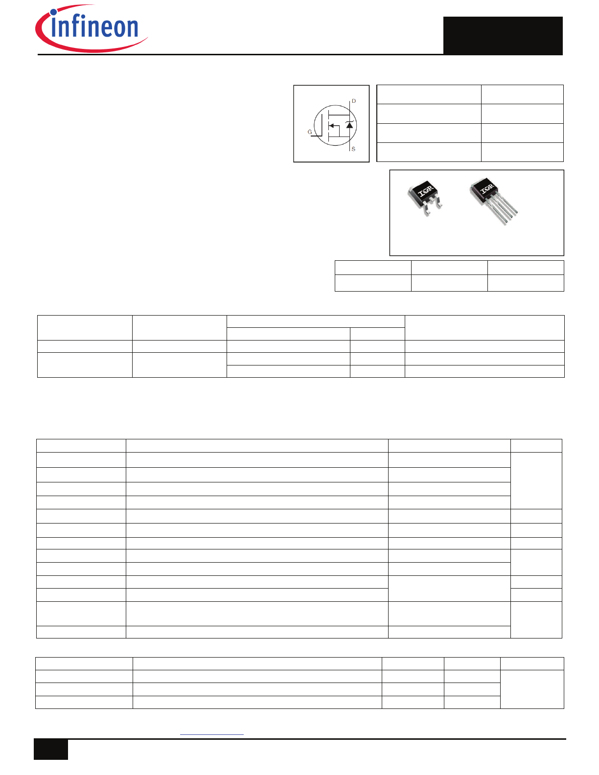
G D S
Gate Drain Source
S
G
D
HEXFET
®
Power MOSFET
G
I-Pak
AUIRFU4104
S
D
D
AUIRFR/U4104
2
2015-12-1
Notes:
Repetitive rating; pulse width limited by max. junction temperature. (See fig. 11)
Limited by
T
Jmax ,
starting T
J
= 25°C, L = 0.16mH, R
G
= 25
, I
AS
= 42A, V
GS
=10V. Part not recommended for use above this value.
Pulse width
1.0ms; duty cycle 2%.
C
oss
eff. is a fixed capacitance that gives the same charging time as C
oss
while V
DS
is rising from 0 to 80% V
DSS
Limited by T
Jmax
, see Fig.12a, 12b, 15, 16 for typical repetitive avalanche performance.
This value determined from sample failure population, starting T
J
= 25°C, L = 0.16mH, R
G
= 25
, I
AS
= 42A, V
GS
=10V.
When mounted on 1" square PCB (FR-4 or G-10 Material). For recommended footprint and soldering techniques refer to
application note #AN-994
R
is measured at T
J
approximately 90°C.
Static @ T
J
= 25°C (unless otherwise specified)
Parameter Min.
Typ.
Max.
Units
Conditions
V
(BR)DSS
Drain-to-Source Breakdown Voltage
40
––– –––
V V
GS
= 0V, I
D
= 250µA
V
(BR)DSS
/
T
J
Breakdown Voltage Temp. Coefficient
––– 0.032 ––– V/°C Reference to 25°C, I
D
= 1mA
R
DS(on)
Static Drain-to-Source On-Resistance
–––
4.3
5.5
m
V
GS
= 10V, I
D
= 42A
V
GS(th)
Gate Threshold Voltage
2.0
–––
4.0
V V
DS
= V
GS
, I
D
= 250µA
gfs
Forward Trans conductance
58
––– –––
S V
DS
= 10V, I
D
= 42A
I
DSS
Drain-to-Source Leakage Current
––– ––– 20
µA
V
DS
= 40V, V
GS
= 0V
––– ––– 250
V
DS
= 40V,V
GS
= 0V,T
J
=125°C
I
GSS
Gate-to-Source Forward Leakage
–––
––– 200
nA
V
GS
= 20V
Gate-to-Source Reverse Leakage
–––
––– -200
V
GS
= -20V
Dynamic Electrical Characteristics @ T
J
= 25°C (unless otherwise specified)
Q
g
Total Gate Charge
–––
59
89
nC
I
D
= 42A
Q
gs
Gate-to-Source Charge
–––
19
–––
V
DS
= 32V
Q
gd
Gate-to-Drain Charge
–––
24
–––
V
GS
= 10V
t
d(on)
Turn-On Delay Time
–––
17
–––
ns
V
DD
= 20V
t
r
Rise Time
–––
69
–––
I
D
= 42A
t
d(off)
Turn-Off Delay Time
–––
37
–––
R
G
= 6.8
t
f
Fall Time
–––
36
–––
V
GS
= 10V
L
D
Internal Drain Inductance
–––
4.5
–––
nH
Between lead,
6mm (0.25in.)
L
S
Internal Source Inductance
–––
7.5
–––
from package
and center of die contact
C
iss
Input Capacitance
––– 2950 –––
pF
V
GS
= 0V
C
oss
Output Capacitance
–––
660 –––
V
DS
= 25V
C
rss
Reverse Transfer Capacitance
–––
370 –––
ƒ = 1.0MHz
C
oss
Output Capacitance
––– 2130 –––
V
GS
= 0V, V
DS
= 1.0V ƒ = 1.0MHz
C
oss
Output Capacitance
–––
590 –––
V
GS
= 0V, V
DS
= 32V ƒ = 1.0MHz
C
oss eff.
Effective Output Capacitance
–––
850 –––
V
GS
= 0V, V
DS
= 0V to 32V
Diode Characteristics
Parameter
Min. Typ. Max. Units
Conditions
I
S
Continuous Source Current
––– ––– 42
A
MOSFET symbol
(Body Diode)
showing the
I
SM
Pulsed Source Current
––– ––– 480
integral reverse
(Body Diode)
p-n junction diode.
V
SD
Diode Forward Voltage
–––
–––
1.3
V T
J
= 25°C,I
S
= 42A, V
GS
= 0V
t
rr
Reverse Recovery Time
–––
28
42
ns T
J
= 25°C ,I
F
= 42A, V
DD
= 20V
Q
rr
Reverse Recovery Charge
–––
24
36
nC di/dt = 100A/µs
t
on
Forward Turn-On Time
Intrinsic turn-on time is negligible (turn-on is dominated by L
S
+L
D
)
AUIRFR/U4104
3
2015-12-1
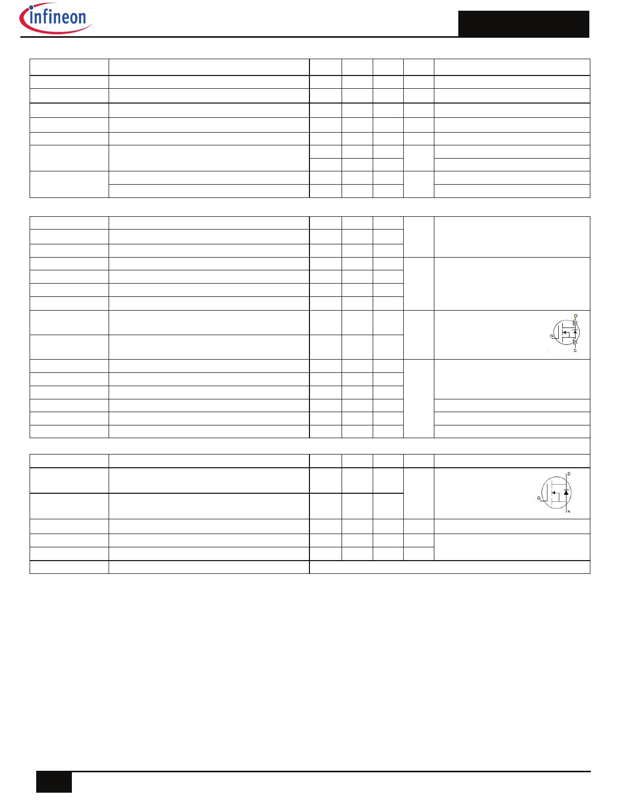
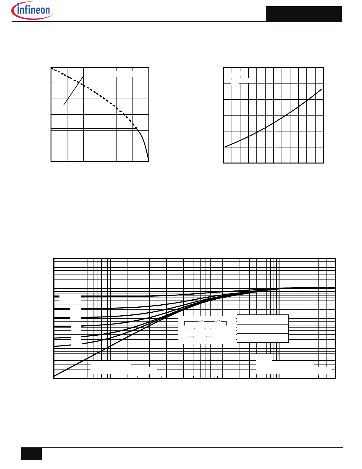
Fig. 2 Typical Output Characteristics
Fig. 3
Typical Transfer Characteristics
Fig. 4
Typical Forward Trans conductance
Vs. Drain Current
Fig. 1 Typical Output Characteristics
0
1
10
100
0.1
1
10
100
VDS, Drain-to-Source Voltage (V)
1
10
100
1000
I D
, D
ra
in
-t
o-
S
ou
rc
e
C
ur
re
nt
(
A
)
60µs PULSE WIDTH
Tj = 25°C
4.5V
0
1
10
100
0.1
1
10
100
VDS, Drain-to-Source Voltage (V)
1
10
100
1000
I D
, D
ra
in
-t
o-
S
ou
rc
e
C
ur
re
nt
(
A
)
60µs PULSE WIDTH
Tj = 175°C
4.5V
V
GS
TOP 15V
10V
8.0V
7.0V
6.0V
5.5V
5.0V
BOTTOM 4.5V
V
GS
TOP 15V
10V
8.0V
7.0V
6.0V
5.5V
5.0V
BOTTOM 4.5V
4
6
8
10
VGS, Gate-to-Source Voltage (V)
1
10
100
1000
I D
, D
ra
in
-t
o-
S
ou
rc
e
C
ur
re
nt
)
VDS = 20V
60µs PULSE WIDTH
TJ = 25°C
TJ = 175°C
0
20
40
60
80
100
ID, Drain-to-Source Current (A)
0
20
40
60
80
100
120
G
fs
,
F
or
w
ar
d
T
ra
ns
co
nd
uc
ta
nc
e
(S
)
TJ = 25°C
TJ = 175°C
VDS = 10V
380µs PULSE WIDTH
AUIRFR/U4104
4
2015-12-1
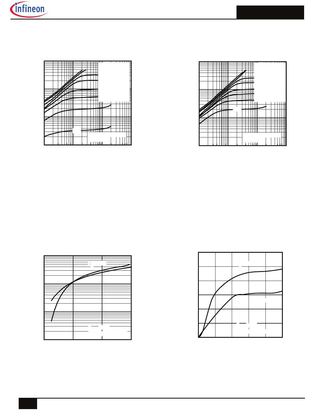
Fig 5. Typical Capacitance vs.
Drain-to-Source Voltage
Fig 6. Typical Gate Charge vs.
Gate-to-Source Voltage
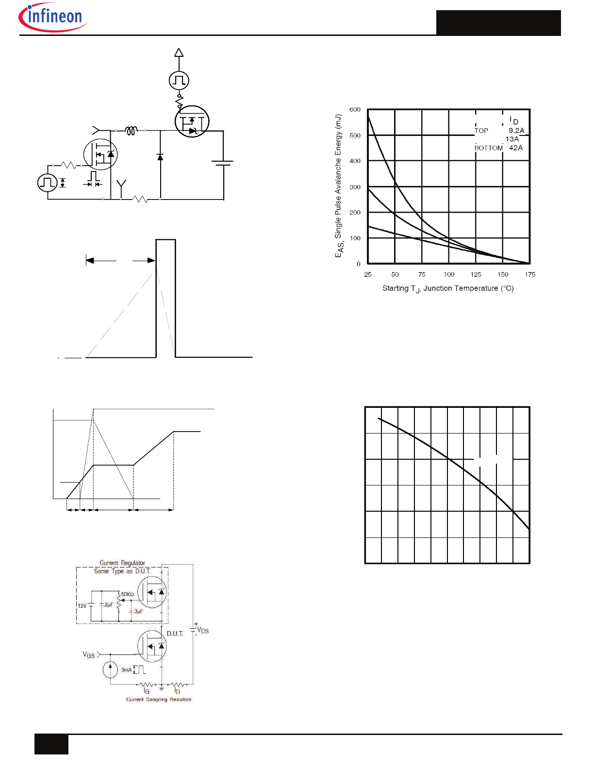
Fig 8. Maximum Safe Operating Area
Fig. 7 Typical Source-to-Drain Diode
Forward Voltage
1
10
100
VDS, Drain-to-Source Voltage (V)
0
1000
2000
3000
4000
5000
C
, C
ap
ac
ita
nc
e
(p
F
)
Coss
Crss
Ciss
VGS = 0V, f = 1 MHZ
Ciss = Cgs + Cgd, C ds SHORTED
Crss = Cgd
Coss = Cds + Cgd
0
20
40
60
80
100
QG Total Gate Charge (nC)
0
4
8
12
16
20
V
G
S
, G
at
e-
to
-S
ou
rc
e
V
ol
ta
ge
(
V
)
VDS= 32V
VDS= 20V
ID= 42A
0.0
0.5
1.0
1.5
2.0
VSD, Source-toDrain Voltage (V)
0.1
1.0
10.0
100.0
1000.0
I S
D
,
R
ev
er
se
D
ra
in
C
ur
re
nt
(
A
)
TJ = 25°C
TJ = 175°C
VGS = 0V
0
1
10
100
1000
VDS , Drain-toSource Voltage (V)
0.1
1
10
100
1000
10000
I D
,
D
ra
in
-t
o-
S
ou
rc
e
C
ur
re
nt
(
A
)
Tc = 25°C
Tj = 175°C
Single Pulse
1msec
10msec
OPERATION IN THIS AREA
LIMITED BY R DS(on)
100µsec
AUIRFR/U4104
5
2015-12-1
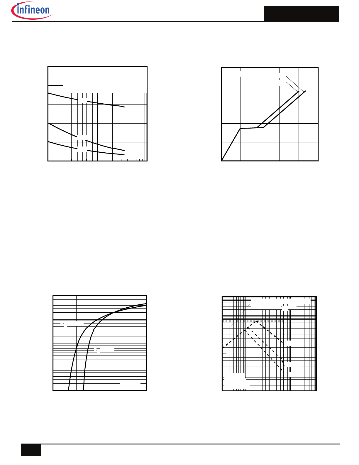
Fig 10. Normalized On-Resistance
Vs. Temperature
Fig 11. Maximum Effective Transient Thermal Impedance, Junction-to-Case
Fig 9. Maximum Drain Current Vs.
Case Temperature
25
50
75
100
125
150
175
TC , Case Temperature (°C)
0
20
40
60
80
100
120
I D
,
D
ra
in
C
ur
re
nt
(
A
)
LIMITED BY PACKAGE
-60 -40 -20 0
20 40 60 80 100 120 140 160 180
TJ , Junction Temperature (°C)
0.5
1.0
1.5
2.0
R
D
S
(o
n)
,
D
ra
in
-t
o-
S
ou
rc
e
O
n
R
es
is
ta
nc
e
(
N
or
m
al
iz
ed
)
ID = 42A
VGS = 10V
1E-006
1E-005
0.0001
0.001
0.01
0.1
t1 , Rectangular Pulse Duration (sec)
0.001
0.01
0.1
1
10
T
he
rm
al
Re
sp
on
se
(
Z
th
JC
)
0.20
0.10
D = 0.50
0.02
0.01
0.05
SINGLE PULSE
( THERMAL RESPONSE )
Notes:
1. Duty Factor D = t1/t2
2. Peak Tj = P dm x Zthjc + Tc
J
J
1
1
2
2
R
1
R
1
R
2
R
2
C
C
Ci=
iRi
Ci=
iRi
Ri (°C/W)
i (sec)
0.5067
0.000414
0.5428
0.004081
AUIRFR/U4104
6
2015-12-1
Fig 12c. Maximum Avalanche Energy
vs. Drain Current
Fig 12a. Unclamped Inductive Test Circuit
Fig 12b. Unclamped Inductive Waveforms
RG
IAS
0.01
tp
D.U.T
L
VDS
+
- VDD
DRIVER
A
15V
20V
tp
V
(BR)DSS
I
AS
Fig 13b. Gate Charge Test Circuit
Fig 13a. Gate Charge Waveform
Vds
Vgs
Id
Vgs(th)
Qgs1 Qgs2
Qgd
Qgodr
Fig 14. Threshold Voltage Vs. Temperature
-75 -50 -25
0
25
50
75 100 125 150 175
TJ , Temperature ( °C )
1.0
2.0
3.0
4.0
V
G
S
(t
h)
G
at
e
th
re
sh
ol
d
V
ol
ta
ge
(
V
)
ID = 250µA
AUIRFR/U4104
7
2015-12-1
Fig 15. Typical Avalanche Current Vs. Pulse width
Notes on Repetitive Avalanche Curves , Figures 15, 16:
(For further info, see AN-1005 at www.infineon.com)
1. Avalanche failures assumption:
Purely a thermal phenomenon and failure occurs at a temperature far in
excess of T
jmax
. This is validated for every part type.
2. Safe operation in Avalanche is allowed as long as T
jmax
is not exceeded.
3. Equation below based on circuit and waveforms shown in Figures 12a, 12b.
4. P
D (ave)
= Average power dissipation per single avalanche pulse.
5. BV = Rated breakdown voltage (1.3 factor accounts for voltage increase
during
avalanche).
6. I
av
= Allowable avalanche current.
7.
T
=
Allowable rise in junction temperature, not to exceed
T
jmax
(assumed as
25°C in Figure 15, 16).
t
av =
Average time in avalanche.
D = Duty cycle in avalanche = t
av
·f
Z
thJC
(D, t
av
) = Transient thermal resistance, see Figures 13)
P
D (ave)
= 1/2 ( 1.3·BV·I
av
) =
T/ Z
thJC
I
av
= 2
T/ [1.3·BV·Z
th
]
E
AS (AR)
= P
D (ave)
·t
av
Fig 16. Maximum Avalanche Energy
Vs. Temperature
1.0E-06
1.0E-05
1.0E-04
1.0E-03
1.0E-02
tav (sec)
0.1
1
10
100
1000
A
va
la
nc
he
C
ur
re
nt
(
A
)
0.05
Duty Cycle = Single Pulse
0.10
Allowed avalanche Current vs
avalanche pulsewidth, tav
assuming Tj = 25°C due to
avalanche losses. Note: In no
case should Tj be allowed to
exceed Tjmax
0.01
25
50
75
100
125
150
175
Starting TJ , Junction Temperature (°C)
0
40
80
120
160
E
A
R
,
A
va
la
nc
he
E
ne
rg
y
(m
J)
TOP Single Pulse
BOTTOM 1% Duty Cycle
ID = 42A
AUIRFR/U4104
8
2015-12-1
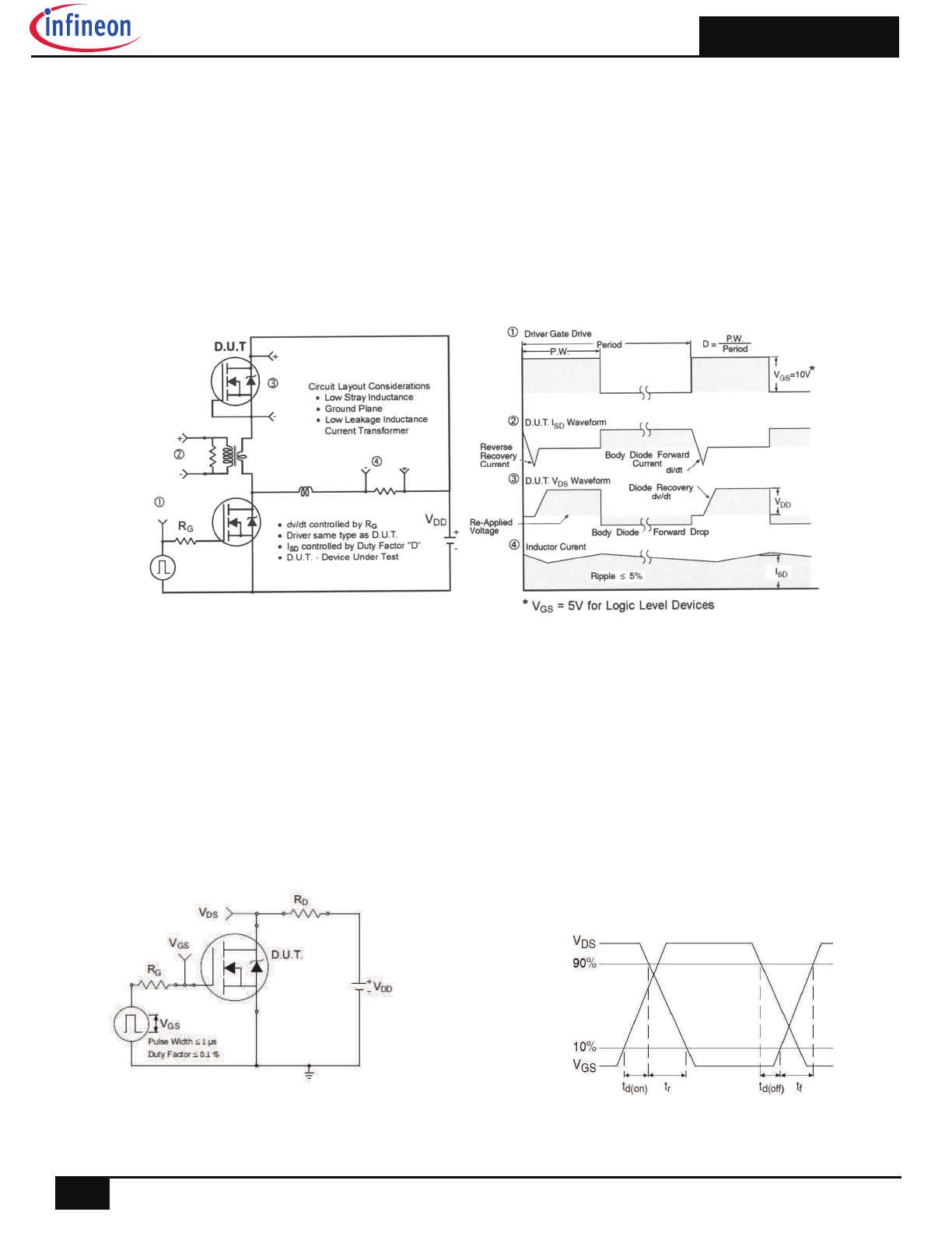
Fig 17. Peak Diode Recovery dv/dt Test Circuit for N-Channel HEXFET® Power MOSFETs
Fig 18a. Switching Time Test Circuit
Fig 18b. Switching Time Waveforms
AUIRFR/U4104
9
2015-12-1
Note: For the most current drawing please refer to IR website at
http://www.irf.com/package/
D-Pak (TO-252AA) Package Outline (Dimensions are shown in millimeters (inches))
YWWA
XX
XX
Date Code
Y= Year
WW= Work Week
AUFR4104
Lot Code
Part Number
IR Logo
D-Pak (TO-252AA) Part Marking Information
AUIRFR/U4104
10
2015-12-1
I-Pak (TO-251AA) Part Marking Information
YWWA
XX
XX
Date Code
Y= Year
WW= Work Week
AUFU4104
Lot Code
Part Number
IR Logo
I-Pak (TO-251AA) Package Outline (Dimensions are shown in millimeters (inches)
Note: For the most current drawing please refer to IR website at
http://www.irf.com/package/