
AUIRF7343Q
V
DSS
55V
R
DS(on)
typ.
0.043
I
D
4.7A
-55V
0.095
-3.4A
N-CH P-CH
max. 0.050
0.105
Description
Specifically designed for Automotive applications, these HEXFET® Power
MOSFET's in a Dual SO-8 package utilize the lastest processing techniques to
achieve extremely low on-resistance per silicon area. Additional features of
these Automotive qualified HEXFET Power MOSFET's are a 150°C junction
operating temperature, fast switching speed and improved repetitive
avalanche rating. These benefits combine to make this design an extremely
efficient and reliable device for use in Automotive applications and a wide
variety of other applications.
The efficient SO-8 package provides enhanced thermal characteristics and
dual MOSFET die capability making it ideal in a variety of power applications.
This dual, surface mount SO-8 can dramatically reduce board space and is
also available in Tape & Reel.
Features
Advanced Planar Technology
Ultra Low On-Resistance
Logic Level Gate Drive
Dual N and P Channel MOSFET
Surface Mount
Available in Tape & Reel
150°C Operating Temperature
Lead-Free, RoHS Compliant
Automotive Qualified *
1
2015-9-30
HEXFET® is a registered trademark of Infineon.
*Qualification standards can be found at
www.infineon.com
AUTOMOTIVE GRADE
Symbol
Parameter
Max.
Units
N-Channel P-Channel
V
DS
Drain-Source
Voltage
55
-55 V
I
D
@ T
A
= 25°C
Continuous Drain Current, V
GS
@ 10V
4.7
-3.4
A
I
D
@ T
A
= 70°C
Continuous Drain Current, V
GS
@ 10V
3.8
-2.7
I
DM
Pulsed Drain Current 38
-27
P
D
@T
A
= 25°C
Maximum Power Dissipation
2.0
W
P
D
@T
A
= 70°C
Maximum Power Dissipation
1.3
E
AS
Single Pulse Avalanche Energy (Thermally Limited)
72
114
mJ
I
AR
Avalanche Current
4.7
-3.4
A
E
AR
Repetitive Avalanche Energy
0.20
mJ
V
GS
Gate-to-Source Voltage
± 20
V
dv/dt
Peak Diode Recovery dv/dt 5.0
-5.0
V/ns
T
J
Operating Junction and
-55 to + 150
°C
T
STG
Storage Temperature Range
Absolute Maximum Ratings
Stresses beyond those listed under “Absolute Maximum Ratings” may cause permanent damage to the device. These are stress
ratings only; and functional operation of the device at these or any other condition beyond those indicated in the specifications is not
implied. Exposure to absolute-maximum-rated conditions for extended periods may affect device reliability. The thermal resistance
and power dissipation ratings are measured under board mounted and still air conditions. Ambient temperature (TA) is 25°C, unless
otherwise specified.
Thermal Resistance
Symbol Parameter
Typ.
Max.
Units
°C/W
R
JA
Junction-to-Ambient ( PCB Mount, steady state) –––
62.5
SO-8
AUIRF7343Q
Base part number
Package Type
Standard Pack
Orderable Part Number
Form
Quantity
AUIRF7343Q
SO-8
Tape and Reel
4000
AUIRF7343QTR
G D S
Gate Drain Source
D1
D1
D2
D2
G1
S2
G2
S1
Top View
8
1
2
3
4
5
6
7
P-CHANNEL MOSFET
N-CHANNEL MOSFET
AUIRF7343Q
2
2015-9-30
Static @ T
J
= 25°C (unless otherwise specified)
Parameter
Min.
Typ.
Max.
Units
Conditions
V
(BR)DSS
Drain-to-Source Breakdown Voltage
N-Ch 55 ––– –––
V
V
GS
= 0V, I
D
= 250µA
P-Ch -55 ––– –––
V
GS
= 0V, I
D
= -250µA
V
(BR)DSS
/
T
J
Breakdown Voltage Temp. Coefficient
N-Ch ––– 0.059 –––
V/°C
Reference to 25°C, I
D
= 1mA
P-Ch
–––
0.054
–––
Reference to 25°C, I
D
= -1mA
R
DS(on)
Static Drain-to-Source On-Resistance
N-Ch
––– 0.043 0.050
V
GS
= 10V, I
D
= 4.7A
––– 0.056 0.065
V
GS
= 4.5V, I
D
= 3.8A
P-Ch
––– 0.095 0.105
V
GS
= -10V, I
D
= -3.4A
––– 0.150 0.170
V
GS
= -4.5V, I
D
= -2.7A
V
GS(th)
Gate Threshold Voltage
N-Ch 1.0 ––– –––
V
V
DS
= V
GS
, I
D
= 250µA
P-Ch -1.0 ––– –––
V
DS
= V
GS
, I
D
= -250µA
gfs
Forward Trans conductance
N-Ch 7.9 ––– –––
S
V
DS
= 10V, I
D
= 4.5A
P-Ch 3.3 ––– –––
V
DS
= -10V, I
D
= -3.1A
I
DSS
Drain-to-Source Leakage Current
N-Ch ––– ––– 2.0
µA
V
DS
= 55V, V
GS
= 0V
P-Ch ––– ––– -2.0
V
DS
= -55V,V
GS
= 0V
N-Ch ––– ––– 25
V
DS
= 55V, V
GS
= 0V ,T
J
= 55°C
P-Ch ––– ––– -25
V
DS
= -55V,V
GS
= 0V,T
J
= 55°C
I
GSS
Gate-to-Source Forward Leakage
N-P
–––
–––
±
100
nA
V
GS
=
±
20V
Gate-to-Source Reverse Leakage
N-P
–––
–––
±
100 V
GS
=
±
20V
Dynamic Electrical Characteristics @ T
J
= 25°C (unless otherwise specified)
Q
g
Total Gate Charge
N-Ch ––– 24 36
nC
N-Channel
P-Ch ––– 26 38
I
D
= 4.5A, V
DS
= 44V,V
GS
= 10V
Q
gs
Gate-to-Source Charge
N-Ch ––– 2.3 3.4
P-Ch ––– 3.0 4.5
P-Channel
Q
gd
Gate-to-Drain Charge
N-Ch ––– 7.0 10
I
D
= - 3.1A,V
DS
= -44V,V
GS
= -10V
P-Ch ––– 8.4 13
t
d(on)
Turn-On Delay Time
N-Ch ––– 8.3 12
ns
N-Channel
P-Ch ––– 14 22
V
DD
= 28V,I
D
= 1.0A,R
G
= 6.0
t
r
Rise Time
N-Ch ––– 3.2 4.8
R
D
= 28
P-Ch ––– 10 15
t
d(off)
Turn-Off Delay Time
N-Ch ––– 32 48
P-Channel
P-Ch ––– 43 64
V
DD
= -28V,I
D
= -1.0A,R
G
= 6.0
t
f
Fall Time
N-Ch ––– 13 20
R
D
= 28
P-Ch ––– 22 32
C
iss
Input Capacitance
N-Ch ––– 740 –––
pF
N-Channel
P-Ch ––– 690 –––
V
GS
= 0V,V
DS
= 25V,ƒ = 1.0MHz
C
oss
Output Capacitance
N-Ch ––– 190 –––
P-Ch ––– 210 –––
P-Channel
C
rss
Reverse Transfer Capacitance
N-Ch ––– 71 –––
V
GS
= 0V,V
DS
= -25V,ƒ = 1.0MHz
P-Ch 86 –––
Diode Characteristics
Parameter
Min.
Typ. Max. Units
Conditions
I
S
Continuous Source Current (Body Diode)
N-Ch ––– ––– 2.0
A
P-Ch ––– ––– -2.0
I
SM
Pulsed Source Current
N-Ch ––– ––– 38
(Body Diode)
P-Ch ––– ––– -27
V
SD
Diode Forward Voltage
N-Ch ––– 0.70 1.2
T
J
= 25°C,I
S
= 2.0A,V
GS
= 0V
P-Ch ––– -0.80 -1.2
T
J
= 25°C,I
S
= -2.0A,V
GS
= 0V
t
rr
Reverse Recovery Time
N-Ch ––– 60 90
ns
N-Channel
P-Ch ––– 54 80
T
J
= 25°C ,I
F
= 2.0A, di/dt = 100A/µs
Q
rr
Reverse Recovery Charge
N-Ch ––– 120 170
nC
P-Channel
P-Ch 85 130
T
J
= 25°C,I
F
= -2.0A, di/dt = 100A/µs
V
Notes:
Repetitive rating; pulse width limited by max. junction temperature. (See Fig. 22)
N-Channel I
SD
4.7A, di/dt 220A/µs, V
DD
V
(BR)DSS
, T
J
150°C.
P-Channel
I
SD
-3.4A, di/dt -150A/µs, V
DD
V
(BR)DSS
, T
J
150°C
N-Channel Starting T
J
= 25°C, L = 6.5mH, R
G
= 25
, I
AS
= 4.7A.
P-Channel Starting T
J
= 25°C, L = 20mH, R
G
= 25
, I
AS
= -3.4A.
Pulse
width
300µs; duty cycle 2%.
Surface mounted on FR-4 board , t
sec.
AUIRF7343Q
3
2015-9-30
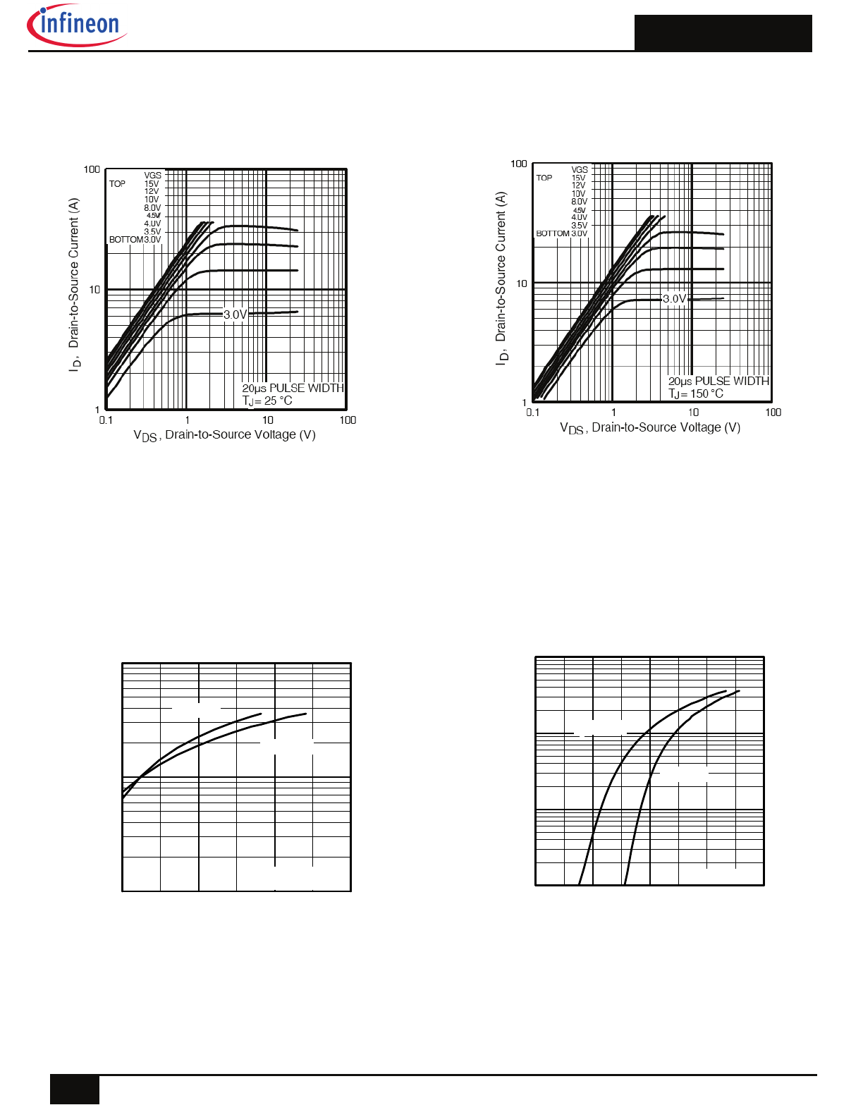
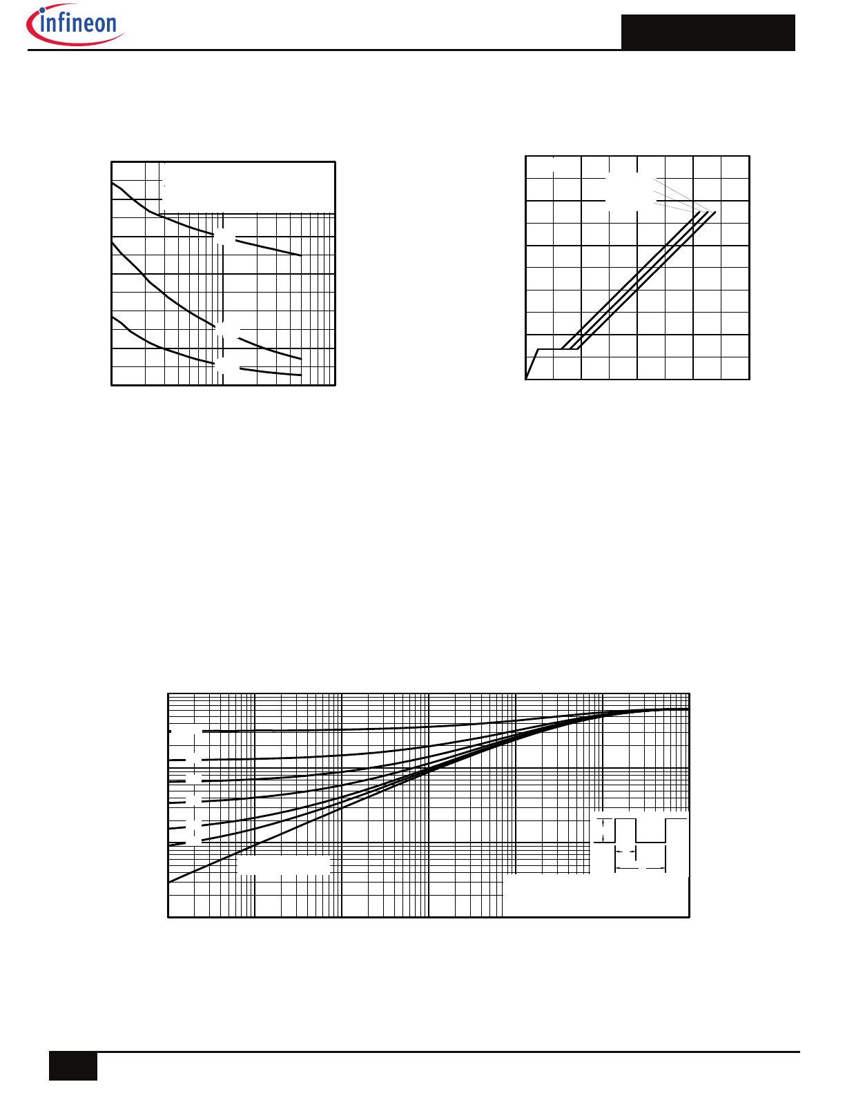
Fig. 2 Typical Output Characteristics
Fig. 3
Typical Transfer Characteristics
Fig. 4 Typical Source-Drain Diode
Forward Voltage
Fig. 1 Typical Output Characteristics
N-Channel
1
10
100
3
4
5
6
V = 25V
20µs PULSE WIDTH
DS
V , Gate-to-Source Voltage (V)
I ,
Drai
n-
to-Sou
rc
e C
urren
t (
A
)
GS
D
T = 25 C
J
°
T = 150 C
J
°
0.1
1
10
100
0.2
0.5
0.8
1.1
1.4
V ,Source-to-Drain Voltage (V)
I
, Re
ve
rse
Dra
in
C
ur
re
nt
(
A
)
SD
SD
V = 0 V
GS
T = 150 C
J
°
T = 25 C
J
°
AUIRF7343Q
4
2015-9-30
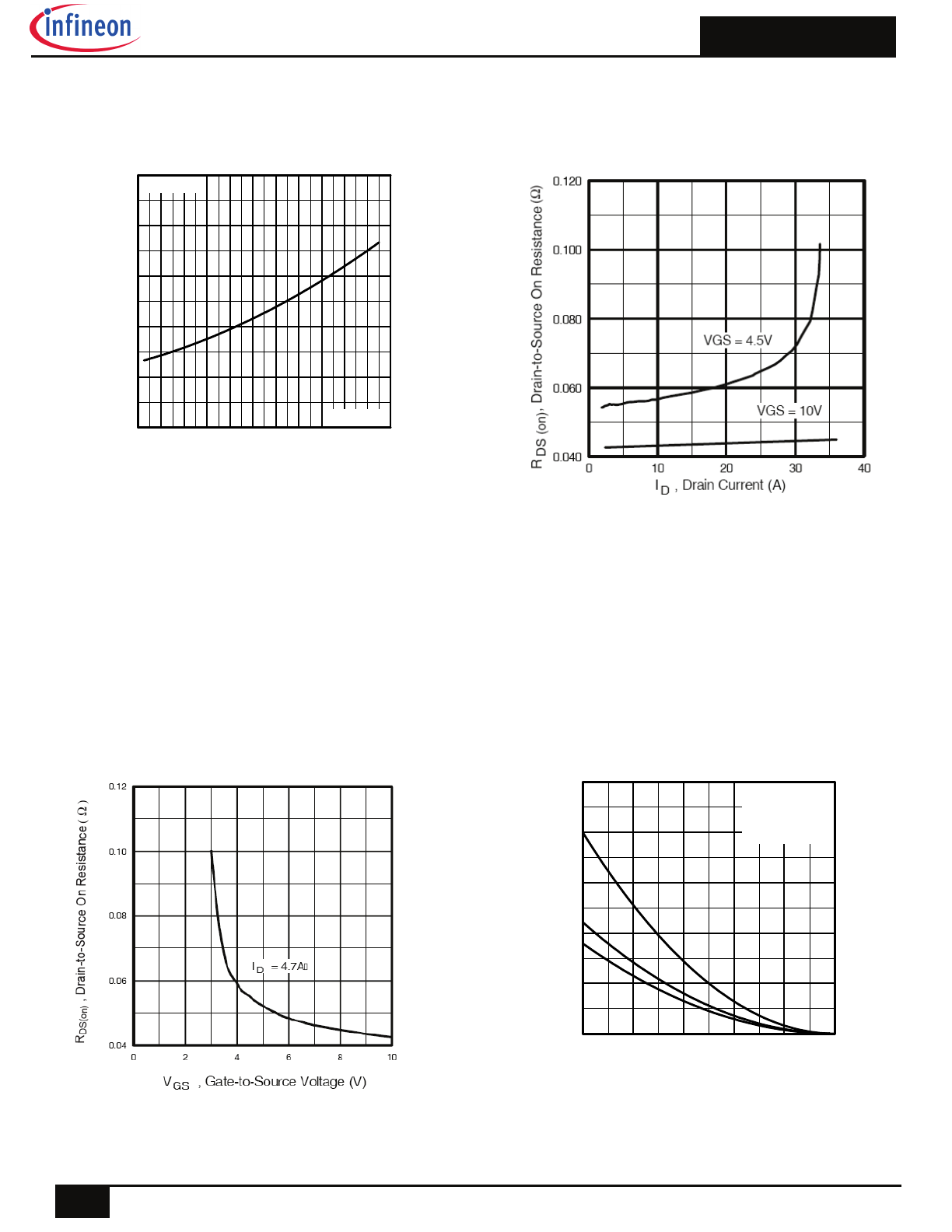
Fig 5.
Normalized On-Resistance
Vs. Temperature
Fig 6.
Typical On-Resistance Vs. Drain
Current
Fig 8. Maximum Avalanche Energy
Vs. Drain Current
Fig. 7 Typical On-Resistance Vs. Gate Voltage
N-Channel
-60 -40 -20
0
20 40 60 80 100 120 140 160
0.0
0.5
1.0
1.5
2.0
2.5
T , Junction Temperature ( C)
R
, Dr
ain-
to-Sou
rce O
n R
esist
ance
(Nor
ma
lized
)
J
DS(
on
)
°
V
=
I =
GS
D
10V
4.7A
25
50
75
100
125
150
0
40
80
120
160
200
Starting T , Junction Temperature ( C)
E
, S
ing
le
P
uls
e A
valan
ch
e
En
erg
y (
m
J)
J
AS
°
ID
TOP
BOTTOM
2.1A
3.8A
4.7A
AUIRF7343Q
5
2015-9-30
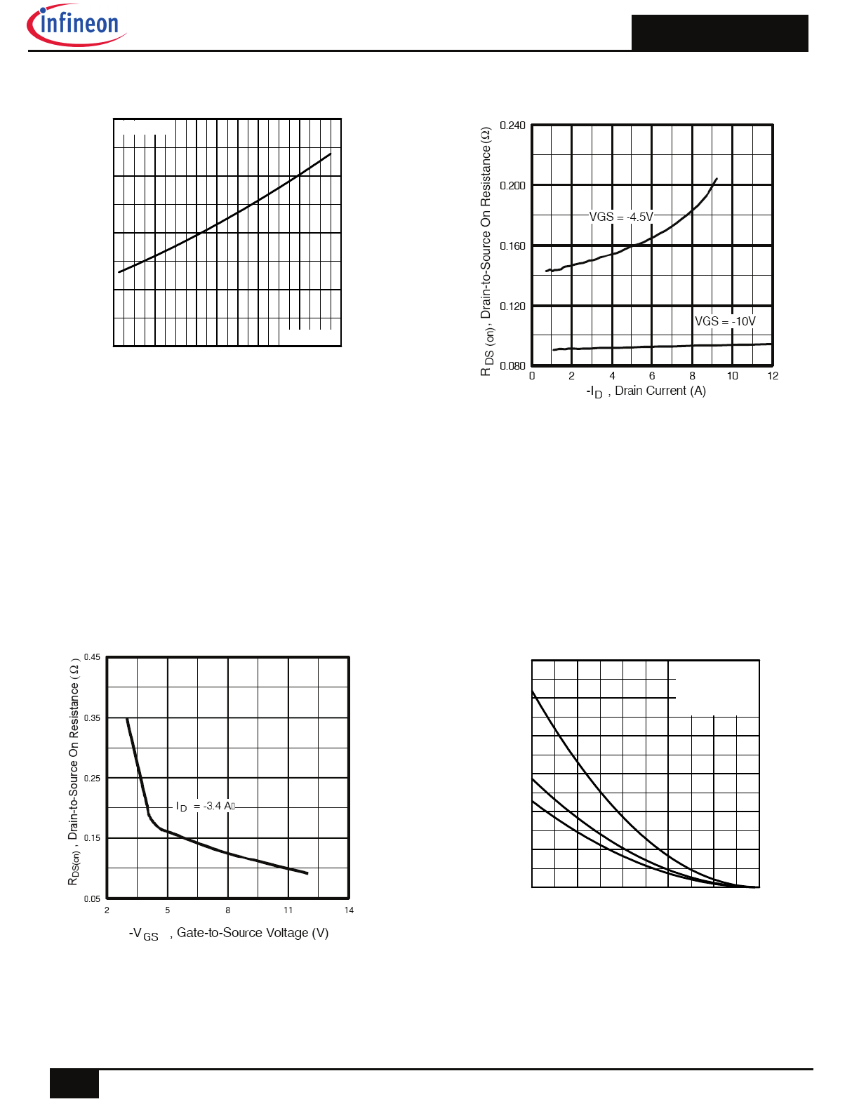
Fig 9.
Typical Capacitance Vs.
Drain-to-Source Voltage
Fig 10.
Typical Gate Charge Vs.
Gate-to-Source
Voltage
Fig 11. Maximum Effective Transient Thermal Impedance, Junction-to-Ambient
N-Channel
1
10
100
0
200
400
600
800
1000
1200
V , Drain-to-Source Voltage (V)
C,
Capac
itan
ce
(
pF)
DS
V
C
C
C
=
=
=
=
0V,
C
C
C
f = 1MHz
+ C
+ C
C SHORTED
GS
iss
gs
gd ,
ds
rss
gd
oss
ds
gd
Ciss
Coss
Crss
0
10
20
30
40
0
4
8
12
16
20
Q , Total Gate Charge (nC)
V
, Gate
-t
o-
Source Volt
ag
e
(V)
G
GS
I =
D
4.5A
V
= 12V
DS
V
= 30V
DS
V
= 48V
DS
0.1
1
10
100
0.0001
0.001
0.01
0.1
1
10
100
Notes:
1. Duty factor D = t / t
2. Peak T = P
x Z
+ T
1
2
J
DM
thJA
A
P
t
t
DM
1
2
t , Rectangular Pulse Duration (sec)
Th
er
ma
l R
e
sp
on
se
(Z
)
1
thJ
A
0.01
0.02
0.05
0.10
0.20
D = 0.50
SINGLE PULSE
(THERMAL RESPONSE)
AUIRF7343Q
6
2015-9-30
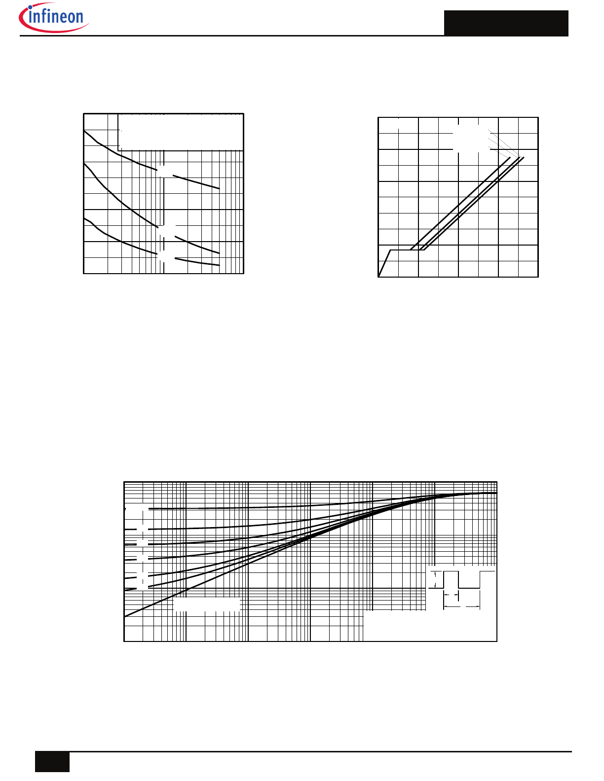
P-Channel
Fig. 13 Typical Output Characteristics
Fig. 14
Typical Transfer Characteristics
Fig. 15 Typical Source-Drain Diode
Forward Voltage
Fig. 12 Typical Output Characteristics
1
10
100
3
4
5
6
7
V = -25V
20µs PULSE WIDTH
DS
-V , Gate-to-Source Voltage (V)
-I
,
Dra
in-
to-
S
ou
rce
C
u
rr
ent
(A
)
GS
D
T = 25 C
J
°
T = 150 C
J
°
0.1
1
10
100
0.2
0.4
0.6
0.8
1.0
1.2
1.4
-V ,Source-to-Drain Voltage (V)
-I
,
Re
ver
se Drai
n
C
urr
ent
(A)
SD
SD
V = 0 V
GS
T = 25 C
J
°
T = 150 C
J
°
AUIRF7343Q
7
2015-9-30
Fig 16.
Normalized On-Resistance
Vs. Temperature
Fig 17.
Typical On-Resistance Vs.
Drain Current
Fig 19. Maximum Avalanche Energy
Vs. Drain Current
Fig. 18 Typical On-Resistance Vs. Gate Voltage
P-Channel
-60 -40 -20
0
20 40 60 80 100 120 140 160
0.0
0.5
1.0
1.5
2.0
T , Junction Temperature( C)
R
, D
ra
in
-to-
S
ourc
e O
n R
es
is
ta
nc
e
(No
rma
liz
ed)
J
D
S
(on)
°
V
=
I =
GS
D
-10V
-3.4 A
25
50
75
100
125
150
0
50
100
150
200
250
300
Starting T , Junction Temperature
( C)
E
, Si
ngl
e
Pu
ls
e
A
vala
nche Ener
gy
(m
J)
J
AS
°
ID
TOP
BOTTOM
-1.5A
-2.7A
-3.4A
AUIRF7343Q
8
2015-9-30
Fig 22. Maximum Effective Transient Thermal Impedance, Junction-to-Ambient
P-Channel
Fig 20. Typical Capacitance Vs.
Drain-to-Source Voltage
Fig 21. Typical Gate Charge Vs.
Gate-to-Source Voltage
1
10
100
0
240
480
720
960
1200
-V , Drain-to-Source Voltage (V)
C,
Capac
itanc
e (
pF)
DS
V
C
C
C
=
=
=
=
0V,
C
C
C
f = 1MHz
+ C
+ C
C SHORTED
GS
iss
gs
gd ,
ds
rss
gd
oss
ds
gd
C
iss
C
oss
C
rss
0
10
20
30
40
0
4
8
12
16
20
Q , Total Gate Charge (nC)
-V
, G
ate
-to
-So
ur
ce
V
olta
ge (
V
)
G
GS
I =
D
-3.1A
V
=-12V
DS
V
=-30V
DS
V
=-48V
DS
0.1
1
10
100
0.0001
0.001
0.01
0.1
1
10
100
Notes:
1. Duty factor D = t / t
2. Peak T = P
x Z
+ T
1
2
J
DM
thJA
A
P
t
t
DM
1
2
t , Rectangular Pulse Duration (sec)
Th
er
m
al
R
e
sp
on
se
(Z
)
1
th
JA
0.01
0.02
0.05
0.10
0.20
D = 0.50
SINGLE PULSE
(THERMAL RESPONSE)
AUIRF7343Q
9
2015-9-30
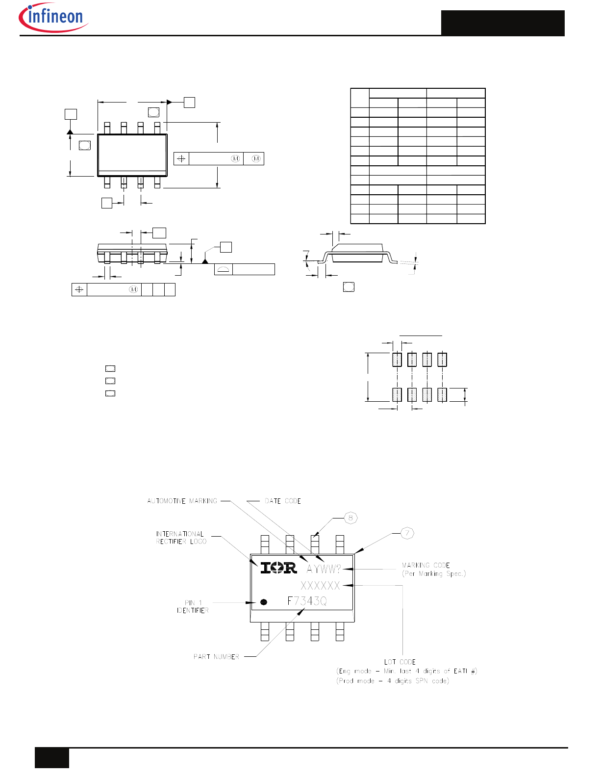
SO-8 Part Marking Information
SO-8 Package Outline
(Dimensions are shown in millimeters (inches)
e 1
D
E
y
b
A
A1
H
K
L
.189
.1497
0°
.013
.050 BASIC
.0532
.0040
.2284
.0099
.016
.1968
.1574
8°
.020
.0688
.0098
.2440
.0196
.050
4.80
3.80
0.33
1.35
0.10
5.80
0.25
0.40
0°
1.27 BASIC
5.00
4.00
0.51
1.75
0.25
6.20
0.50
1.27
M IN
M AX
M ILLIM ETERS
IN C H ES
M IN
M AX
D IM
8°
e
c
.0075
.0098
0.19
0.25
.025 BASIC
0.635 BASIC
8
7
5
6
5
D
B
E
A
e
6X
H
0.25 [ .010]
A
6
7
K x 45°
8X L
8X c
y
0.25 [ .010]
C A B
e1
A
A1
8X b
C
0.10 [ .004]
4
3
1
2
F O O T P R I N T
8 X 0 . 7 2 [ . 0 2 8 ]
6 . 4 6 [ . 2 5 5 ]
3 X 1 . 2 7 [ . 0 5 0 ]
4 . O U T L I N E C O N F O R M S T O J E D E C O U T L I N E M S - 0 1 2 A A .
N O T E S :
1 . D I M E N S I O N I N G & T O L E R A N C I N G P E R A S M E Y 1 4 . 5 M - 1 9 9 4 .
2 . C O N T R O L L I N G D I M E N S I O N : M I L L I M E T E R
3 . D I M E N S I O N S A R E S H O W N I N M I L L I M E T E R S [ I N C H E S ] .
5 D I M E N S I O N D O E S N O T I N C L U D E M O L D P R O T R U S I O N S .
6 D I M E N S I O N D O E S N O T I N C L U D E M O L D P R O T R U S I O N S .
M O L D P R O T R U S I O N S N O T T O E X C E E D 0 . 2 5 [ . 0 1 0 ] .
7 D I M E N S I O N I S T H E L E N G T H O F L E A D F O R S O L D E R I N G T O
A S U B S T R A T E .
M O L D P R O T R U S I O N S N O T T O E X C E E D 0 . 1 5 [ . 0 0 6 ] .
8 X 1 . 7 8 [ . 0 7 0 ]
AUIRF7343Q
10
2015-9-30
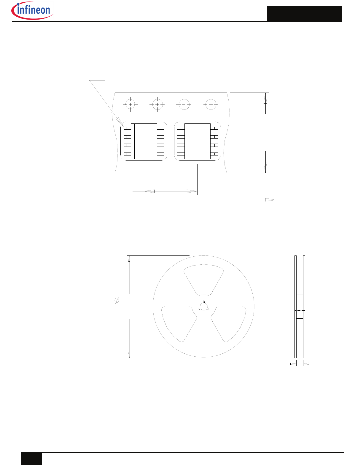
SO-8 Tape and Reel (
Dimensions are shown in millimeters (inches)
330.00
(12.992)
MAX.
14.40 ( .566 )
12.40 ( .488 )
NOTES :
1. CONTROLLING DIMENSION : MILLIMETER.
2. OUTLINE CONFORMS TO EIA-481 & EIA-541.
FEED DIRECTION
TERMINAL NUMBER 1
12.3 ( .484 )
11.7 ( .461 )
8.1 ( .318 )
7.9 ( .312 )
NOTES:
1. CONTROLLING DIMENSION : MILLIMETER.
2. ALL DIMENSIONS ARE SHOWN IN MILLIMETERS(INCHES).
3. OUTLINE CONFORMS TO EIA-481 & EIA-541.