
AUIRF7309Q
V
DSS
30V
R
DS(on)
max. 0.05
I
D
4.7A
-30V
0.10
-3.5A
N-CH P-CH
Description
Specifically designed for Automotive applications, this cellular
design of HEXFET® Power MOSFETs utilizes the latest
processing techniques to achieve low on-resistance per silicon
area. This benefit combined with the fast switching speed and
ruggedized device design that HEXFET power MOSFETs are
well known for, provides the designer with an extremely efficient
and reliable device for use in Automotive and a wide variety of
other applications.
Features
Advanced Planar Technology
Low
On-Resistance
Logic Level Gate Drive
Dual N and P Channel MOSFET
Dynamic dv/dt Rating
150°C Operating Temperature
Fast Switching
Lead-Free, RoHS Compliant
Automotive Qualified *
1
2015-9-30
HEXFET® is a registered trademark of Infineon.
*Qualification standards can be found at
www.infineon.com
AUTOMOTIVE GRADE
Symbol
Parameter
Max.
Units
N-Channel P-Channel
I
D
@ T
A
= 25°C
10 Sec. Pulsed Drain Current, V
GS
@ 10V
4.7
-3.5
A
I
D
@ T
A
= 25°C
Continuous Drain Current, V
GS
@ 10V
4.0
-3.0
I
D
@ T
A
= 70°C
Continuous Drain Current, V
GS
@ 10V
3.2
-2.4
I
DM
Pulsed Drain Current 16
-12
P
D
@T
A
= 25°C
Maximum Power Dissipation
1.4
W
Linear Derating Factor
0.011
W/°C
V
GS
Gate-to-Source Voltage
± 20
V
dv/dt
Peak Diode Recovery dv/dt 6.9
-6.0
V/ns
T
J
Operating Junction and
°C
T
STG
Storage Temperature Range
-55 to + 150
Absolute Maximum Ratings
Stresses beyond those listed under “Absolute Maximum Ratings” may cause permanent damage to the device. These are stress
ratings only; and functional operation of the device at these or any other condition beyond those indicated in the specifications is not
implied. Exposure to absolute-maximum-rated conditions for extended periods may affect device reliability. The thermal resistance
and power dissipation ratings are measured under board mounted and still air conditions. Ambient temperature (TA) is 25°C, unless
otherwise specified.
Thermal Resistance
Symbol Parameter
Typ.
Max.
Units
°C/W
R
JA
Junction-to-Ambient ( PCB Mount, steady state) –––
90
SO-8
AUIRF7309Q
Base part number
Package Type
Standard Pack
Orderable Part Number
Form
Quantity
AUIRF7309Q
SO-8
Tape and Reel
4000
AUIRF7309QTR
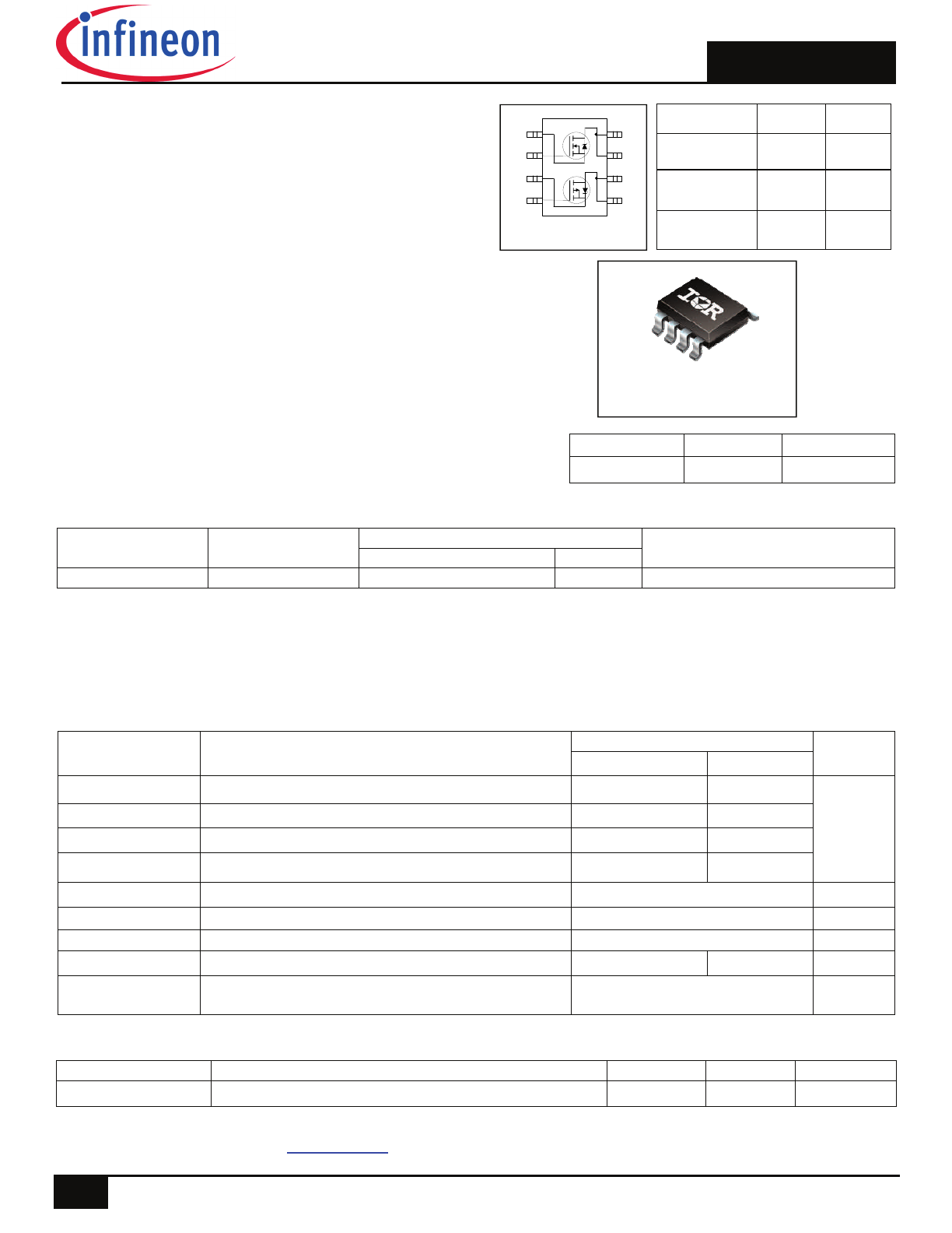
G D S
Gate Drain Source
D1
D1
D2
D2
G1
S2
G2
S1
Top View
8
1
2
3
4
5
6
7
P-CHANNEL MOSFET
N-CHANNEL MOSFET
AUIRF7309Q
2
2015-9-30
Static @ T
J
= 25°C (unless otherwise specified)
Parameter
Min.
Typ.
Max.
Units
Conditions
V
(BR)DSS
Drain-to-Source Breakdown Voltage
N-Ch 30 ––– –––
V
V
GS
= 0V, I
D
= 250µA
P-Ch -30 ––– –––
V
GS
= 0V, I
D
= -250µA
V
(BR)DSS
/
T
J
Breakdown Voltage Temp. Coefficient
N-Ch ––– 0.032 –––
V/°C
Reference to 25°C, I
D
= 1mA
P-Ch
–––
-0.037 –––
Reference to 25°C, I
D
= -1mA
R
DS(on)
Static Drain-to-Source On-Resistance
N-Ch
––– ––– 0.050
V
GS
= 10V, I
D
= 2.4A
––– ––– 0.080
V
GS
= 4.5V, I
D
= 2.0A
P-Ch
––– ––– 0.10
V
GS
= -10V, I
D
= -1.8A
––– ––– 0.16
V
GS
= -4.5V, I
D
= -1.5A
V
GS(th)
Gate Threshold Voltage
N-Ch 1.0 ––– 3.0
V
V
DS
= V
GS
, I
D
= 250µA
P-Ch -1.0 ––– -3.0
V
DS
= V
GS
, I
D
= -250µA
gfs
Forward Trans conductance
N-Ch 5.2 ––– –––
S
V
DS
= 15V, I
D
= 2.4A
P-Ch 2.5 ––– –––
V
DS
= -24V, I
D
= -1.8A
I
DSS
Drain-to-Source Leakage Current
N-Ch ––– ––– 1.0
µA
V
DS
=24V, V
GS
= 0V
P-Ch ––– ––– -1.0
V
DS
= -24V,V
GS
= 0V
N-Ch ––– ––– 25
V
DS
=24V, V
GS
= 0V ,T
J
=125°C
P-Ch ––– ––– -25
V
DS
= -24V,V
GS
= 0V,T
J
=125°C
I
GSS
Gate-to-Source Forward Leakage
N-P
–––
–––
±
100
nA
V
GS
=
±
20V
Gate-to-Source Reverse Leakage
N-P
–––
–––
±
100 V
GS
=
±
20V
Dynamic Electrical Characteristics @ T
J
= 25°C (unless otherwise specified)
Q
g
Total Gate Charge
N-Ch ––– ––– 25
nC
N-Channel
P-Ch ––– ––– 25
I
D
= 2.6A, V
DS
= 16V,V
GS
= 4.5V
Q
gs
Gate-to-Source Charge
N-Ch ––– ––– 2.9
P-Ch ––– ––– 2.9
P-Channel
Q
gd
Gate-to-Drain Charge
N-Ch ––– ––– 7.9
I
D
= -2.2A,V
DS
= -16V,V
GS
= -4.5V
P-Ch ––– ––– 9.0
t
d(on)
Turn-On Delay Time
N-Ch ––– 6.8 –––
ns
N-Channel
P-Ch ––– 11 –––
V
DD
= 10V,I
D
= 2.6A,R
G
= 6.0
t
r
Rise Time
N-Ch ––– 21 –––
R
D
= 3.8
P-Ch ––– 17 –––
t
d(off)
Turn-Off Delay Time
N-Ch ––– 22 –––
P-Channel
P-Ch ––– 25 –––
V
DD
= -10V,I
D
= -2.2A,R
G
= 6.0
t
f
Fall Time
N-Ch ––– 7.7 –––
R
D
= 4.5
P-Ch ––– 18 –––
L
D
Internal Drain Inductance
N-P
–––
4.0
–––
nH
Between lead, 6mm(0.25n) from
L
S
Internal Source Inductance
N-P
–––
6.0
–––
package and center of die contact
C
iss
Input Capacitance
N-Ch ––– 520 –––
pF
N-Channel
P-Ch ––– 440 –––
V
GS
= 0V,V
DS
= 15V,ƒ = 1.0MHz
C
oss
Output Capacitance
N-Ch ––– 180 –––
P-Ch ––– 200 –––
P-Channel
C
rss
Reverse Transfer Capacitance
N-Ch ––– 72 –––
V
GS
= 0V,V
DS
= -15V,ƒ = 1.0MHz
P-Ch 93 –––
Diode Characteristics
Parameter
Min.
Typ. Max. Units
Conditions
I
S
Continuous Source Current (Body Diode)
N-Ch ––– ––– 1.8
A
P-Ch ––– ––– -1.8
I
SM
Pulsed Source Current
N-Ch ––– ––– 16
(Body Diode)
P-Ch ––– ––– -12
V
SD
Diode Forward Voltage
N-Ch ––– ––– 1.0
T
J
= 25°C,I
S
= 1.8A,V
GS
= 0V
P-Ch ––– ––– -1.0
T
J
= 25°C,I
S
= -1.8A,V
GS
= 0V
t
rr
Reverse Recovery Time
N-Ch ––– 47 71
ns
N-Channel
P-Ch ––– 53 80
T
J
= 25°C ,I
F
= 2.6A, di/dt = 100A/µs
Q
rr
Reverse Recovery Charge
N-Ch ––– 56 84
nC
P-Channel
P-Ch 66 99
T
J
= 25°C,I
F
= -2.2A, di/dt = 100A/µs
t
on
Forward Turn-On Time
Intrinsic turn-on time is negligible (turn-on is dominated by L
S
+L
D
)
V
Notes:
Repetitive rating; pulse width limited by max. junction temperature. (See Fig. 23)
N-Channel I
SD
2.4A, di/dt 73A/µs, V
DD
V
(BR)DSS
, T
J
150°C.
P-Channel
I
SD
-1.8A, di/dt 90A/µs, V
DD
V
(BR)DSS
, T
J
150°C
Pulse
width
300µs; duty cycle 2%.
When mounted on 1" square PCB (FR-4 or G-10 Material). For recommended footprint and soldering techniques refer to
application note #AN-994
AUIRF7309Q
3
2015-9-30
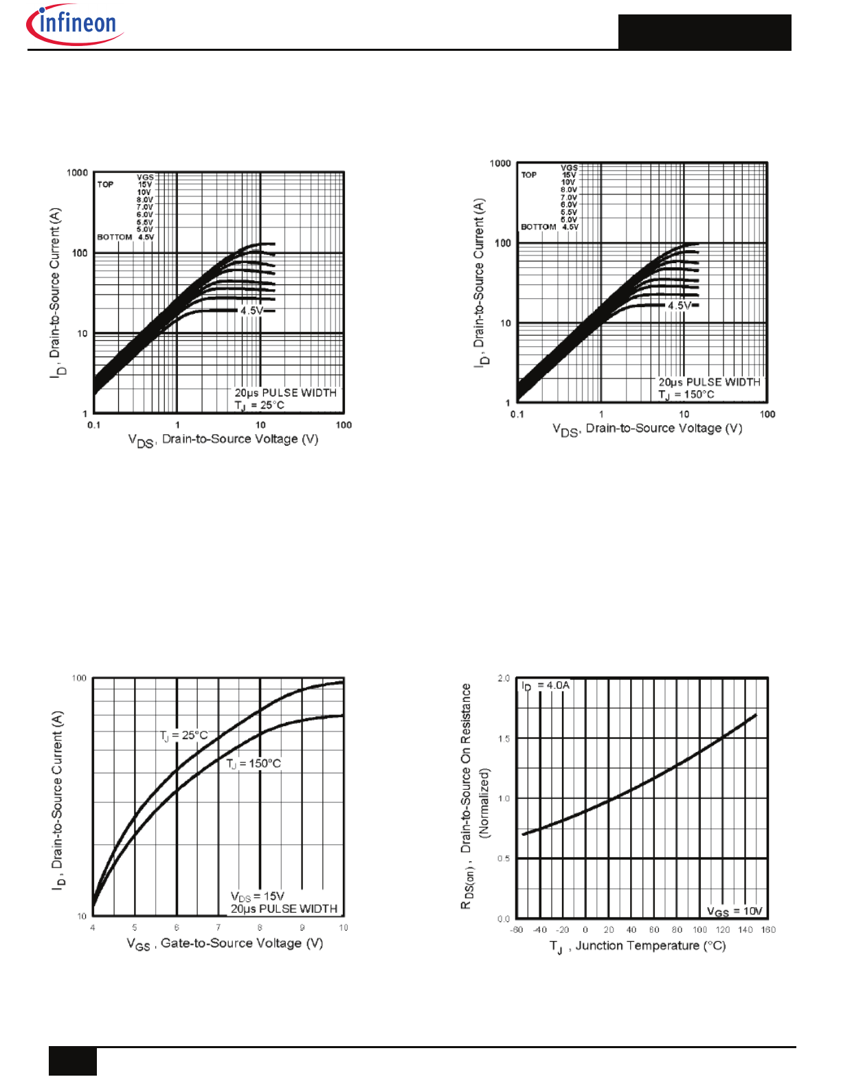
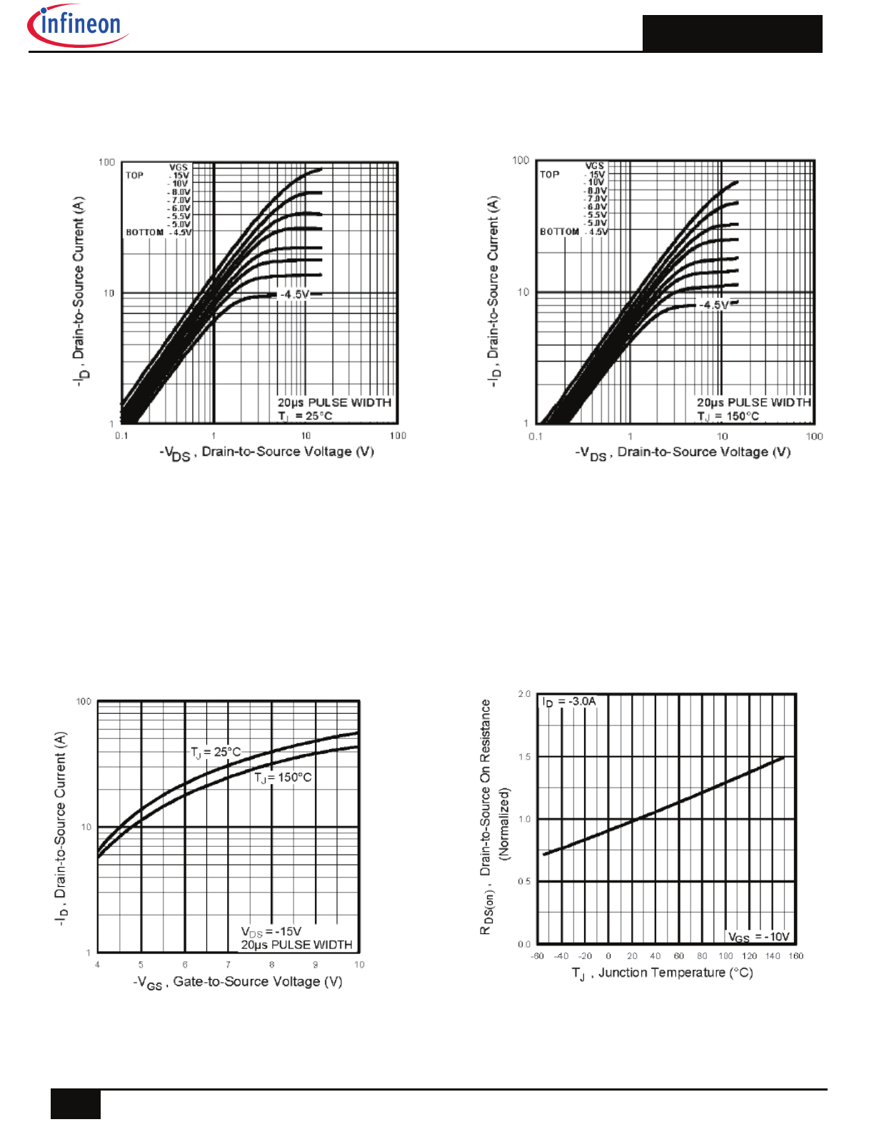
Fig. 2 Typical Output Characteristics
T
J
= 150°C
Fig. 3
Typical Transfer Characteristics
Fig. 4 Normalized On-Resistance
vs. Temperature
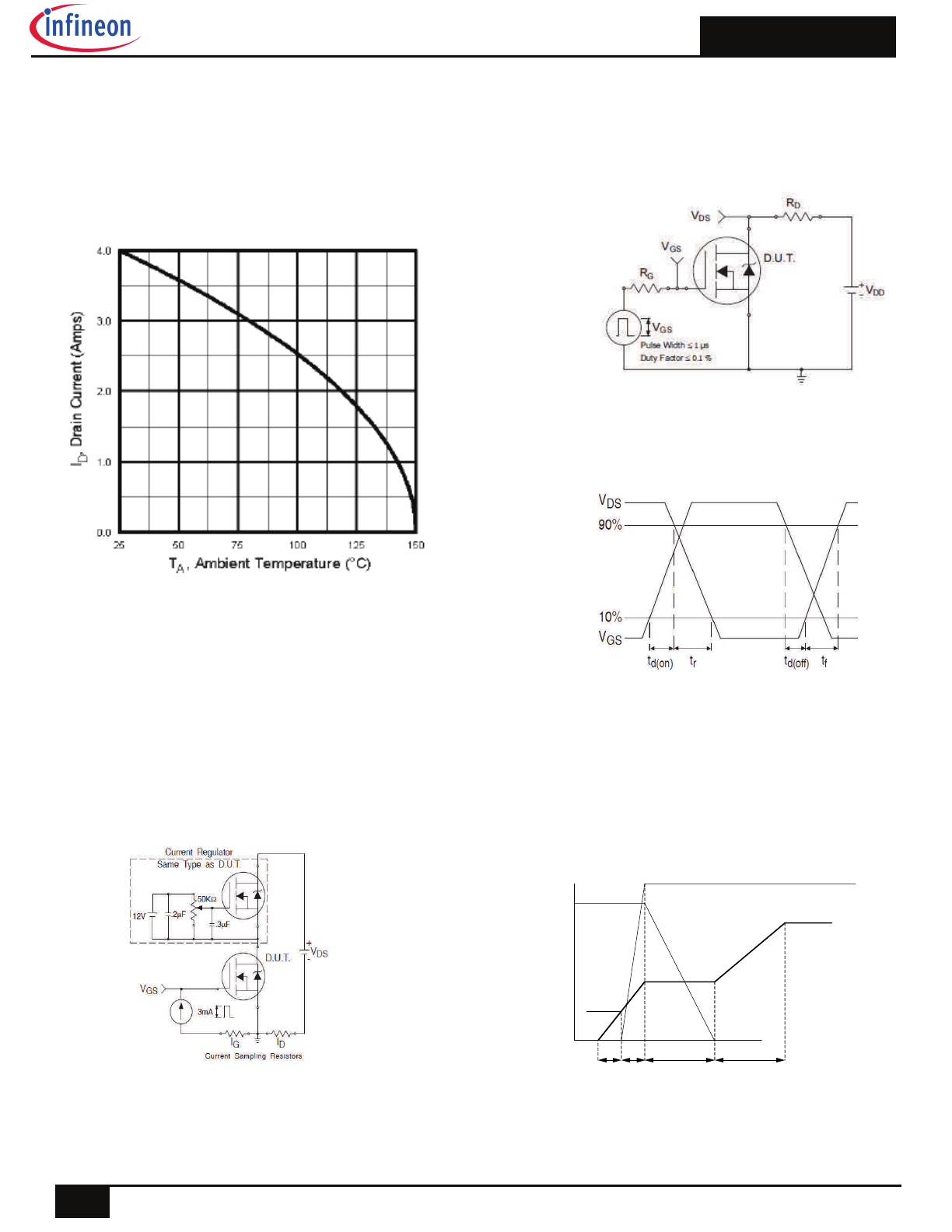
Fig. 1 Typical Output Characteristics
T
J
= 25°C
N-Channel
AUIRF7309Q
4
2015-9-30
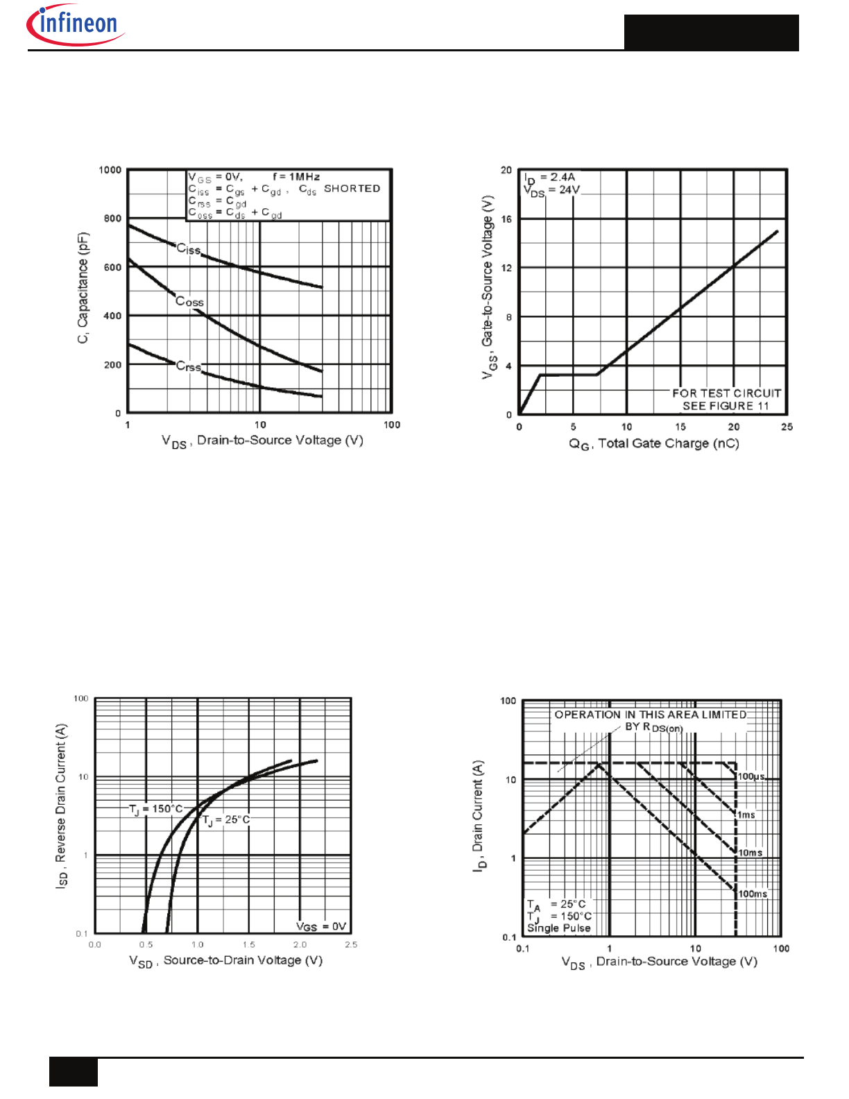
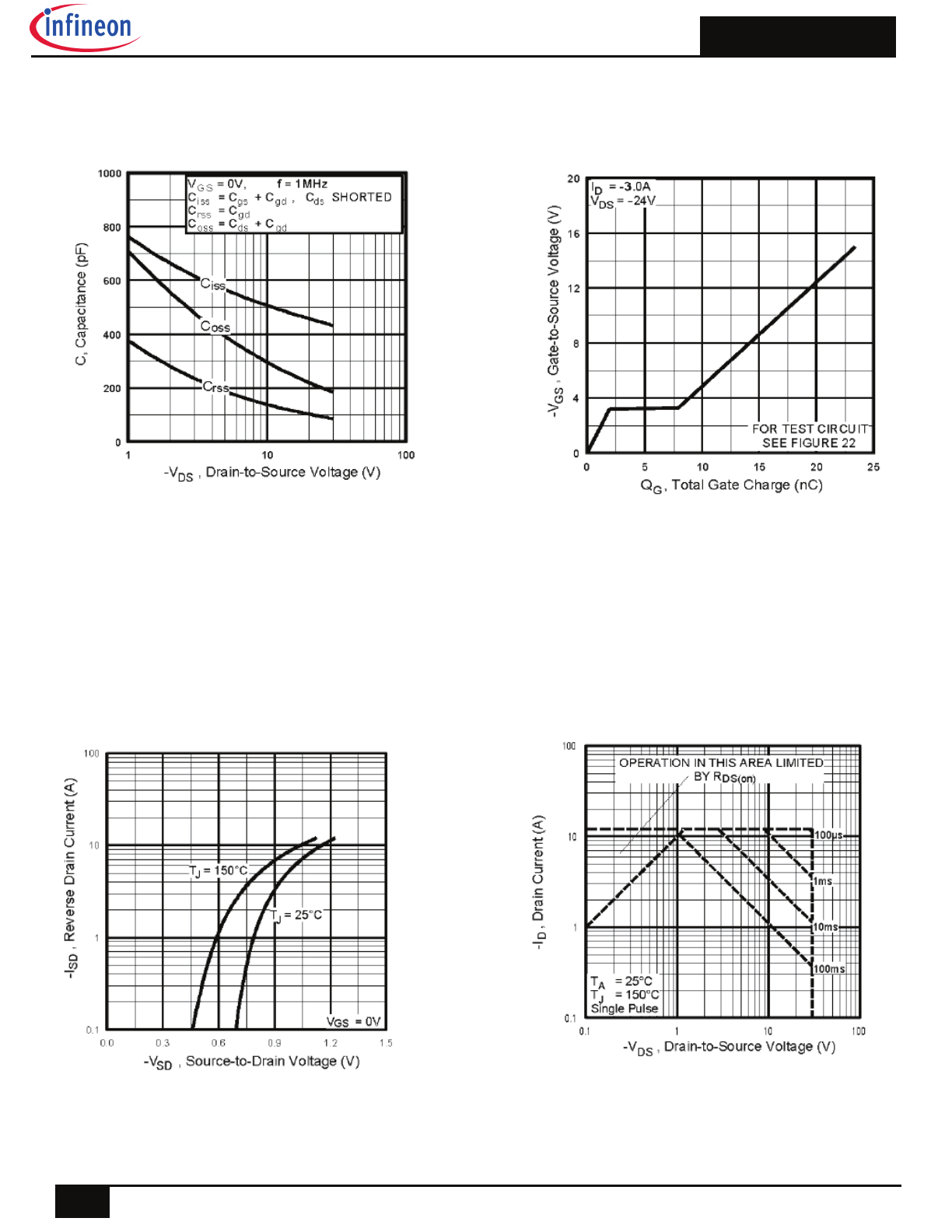
Fig 5. Typical Capacitance vs.
Drain-to-Source Voltage
Fig 6. Typical Gate Charge vs.
Gate-to-Source Voltage
Fig 8. Maximum Safe Operating Area
Fig. 7 Typical Source-to-Drain Diode
Forward Voltage
N-Channel
AUIRF7309Q
5
2015-9-30
Fig 11. Maximum Effective Transient Thermal Impedance, Junction-to-Case
Fig 9. Maximum Drain Current vs. Case Temperature
Fig 10a. Switching Time Test Circuit
Fig 10b. Switching Time Waveforms
Fig 11a. Gate Charge Test Circuit
Vds
Vgs
Id
Vgs(th)
Qgs1 Qgs2
Qgd
Qgodr
Fig 11b. Basic Gate Charge Waveform
N-Channel
AUIRF7309Q
6
2015-9-30
P-Channel
Fig. 13 Typical Output Characteristics
T
J
= 150°C
Fig. 14
Typical Transfer Characteristics
Fig. 15 Normalized On-Resistance
vs. Temperature
Fig. 12 Typical Output Characteristics
T
J
= 25°C
AUIRF7309Q
7
2015-9-30
Fig 16. Typical Capacitance vs.
Drain-to-Source Voltage
Fig 17. Typical Gate Charge vs.
Gate-to-Source Voltage
Fig 19. Maximum Safe Operating Area
Fig. 18 Typical Source-to-Drain Diode
Forward Voltage
P-Channel
AUIRF7309Q
8
2015-9-30
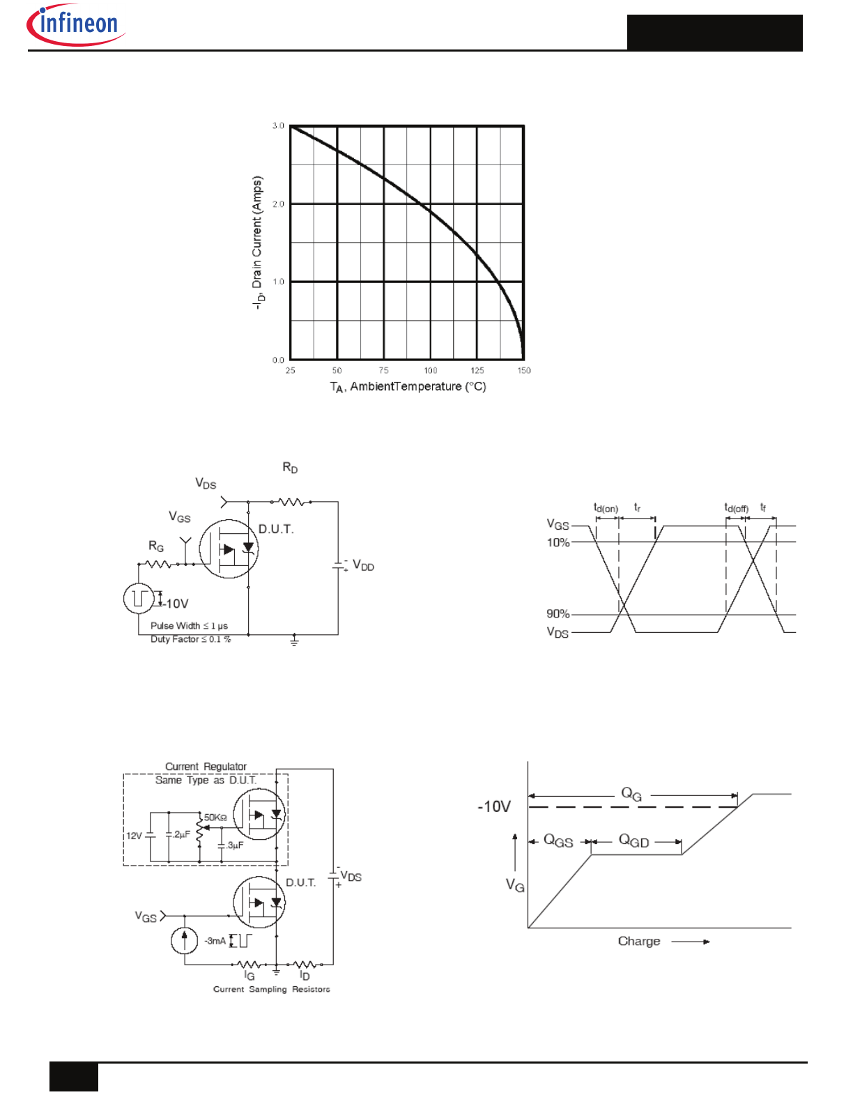
Fig 20. Maximum Drain Current vs. Case Temperature
Fig 21a. Switching Time Test Circuit
Fig 21b. Switching Time Waveforms
Fig 22a. Gate Charge Test Circuit
Fig 22b. Basic Gate Charge Waveform
P-Channel
AUIRF7309Q
9
2015-9-30
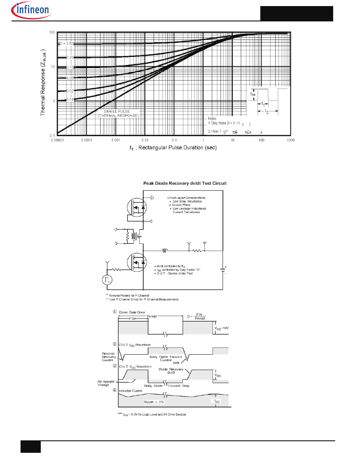
Fig 24. Peak Diode Recovery dv/dt Test Circuit for N & P-Channel HEXFET
®
Power MOSFETs
Fig 23. Maximum Effective Transient Thermal Impedance, Junction-to-Ambient
N and P-Channel
AUIRF7309Q
10
2015-9-30
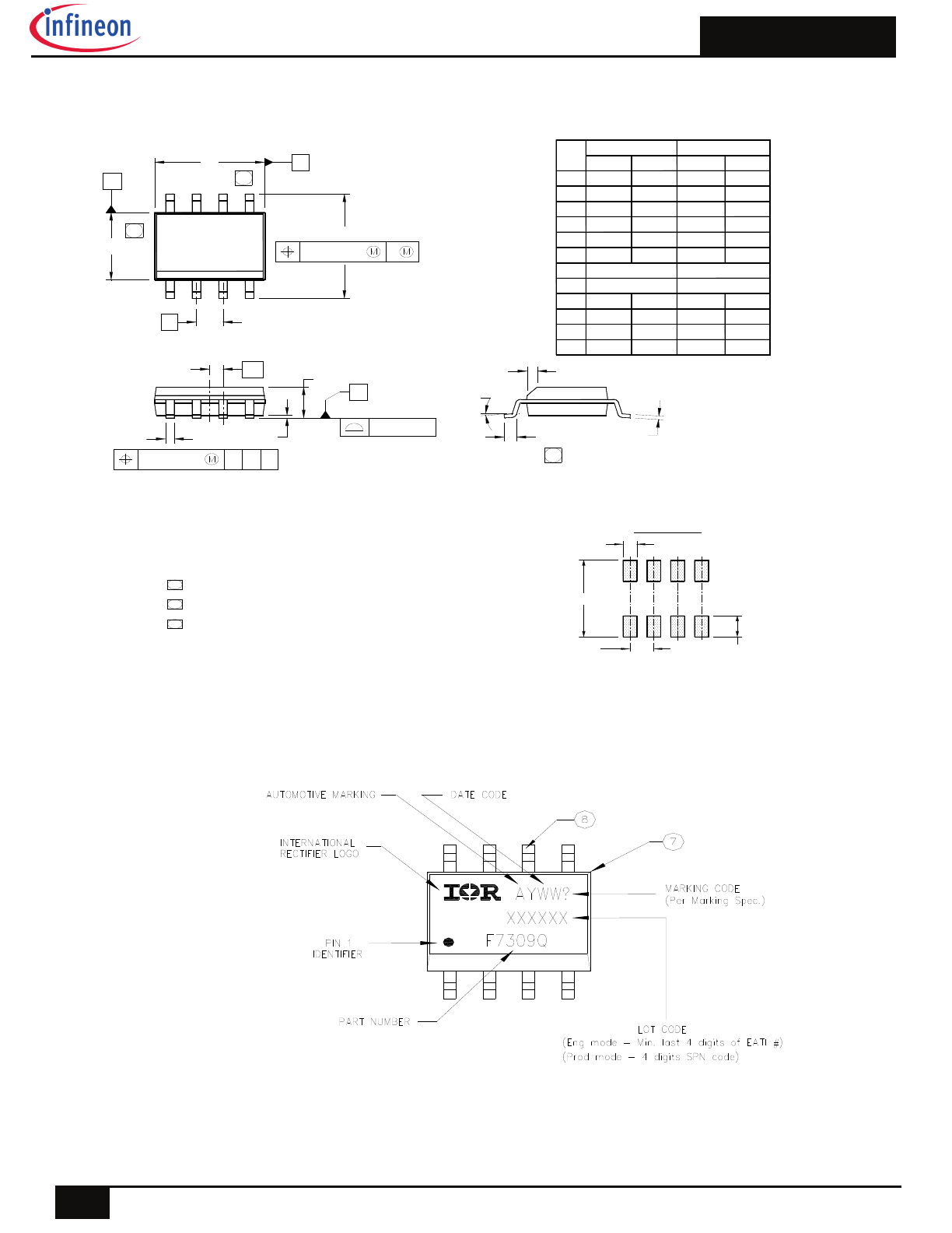
SO-8 Part Marking Information
SO-8 Package Outline
(Dimensions are shown in millimeters (inches)
e 1
D
E
y
b
A
A1
H
K
L
.189
.1497
0°
.013
.050 BASIC
.0532
.0040
.2284
.0099
.016
.1968
.1574
8°
.020
.0688
.0098
.2440
.0196
.050
4.80
3.80
0.33
1.35
0.10
5.80
0.25
0.40
0°
1.27 BASIC
5.00
4.00
0.51
1.75
0.25
6.20
0.50
1.27
M IN
M AX
M ILLIM ETERS
IN C H ES
M IN
M AX
D IM
8°
e
c
.0075
.0098
0.19
0.25
.025 BASIC
0.635 BASIC
8
7
5
6
5
D
B
E
A
e
6X
H
0.25 [ .010]
A
6
7
K x 45°
8X L
8X c
y
0.25 [ .010]
C A B
e1
A
A1
8X b
C
0.10 [ .004]
4
3
1
2
F O O T P R I N T
8 X 0 . 7 2 [ . 0 2 8 ]
6 . 4 6 [ . 2 5 5 ]
3 X 1 . 2 7 [ . 0 5 0 ]
4 . O U T L I N E C O N F O R M S T O J E D E C O U T L I N E M S - 0 1 2 A A .
N O T E S :
1 . D I M E N S I O N I N G & T O L E R A N C I N G P E R A S M E Y 1 4 . 5 M - 1 9 9 4 .
2 . C O N T R O L L I N G D I M E N S I O N : M I L L I M E T E R
3 . D I M E N S I O N S A R E S H O W N I N M I L L I M E T E R S [ I N C H E S ] .
5 D I M E N S I O N D O E S N O T I N C L U D E M O L D P R O T R U S I O N S .
6 D I M E N S I O N D O E S N O T I N C L U D E M O L D P R O T R U S I O N S .
M O L D P R O T R U S I O N S N O T T O E X C E E D 0 . 2 5 [ . 0 1 0 ] .
7 D I M E N S I O N I S T H E L E N G T H O F L E A D F O R S O L D E R I N G T O
A S U B S T R A T E .
M O L D P R O T R U S I O N S N O T T O E X C E E D 0 . 1 5 [ . 0 0 6 ] .
8 X 1 . 7 8 [ . 0 7 0 ]