
AUIRF2805S
AUIRF2805L
V
DSS
55V
R
DS(on)
typ.
3.9m
max.
4.7m
I
D
135A
Features
Advanced Process Technology
Ultra Low On-Resistance
Dynamic dv/dt Rating
175°C Operating Temperature
Fast Switching
Fully Avalanche Rated
Repetitive Avalanche Allowed up to Tjmax
Lead-Free, RoHS Compliant
Automotive Qualified *
Description
Specifically designed for Automotive applications, this
HEXFET® Power MOSFET utilizes the latest processing
techniques to achieve extremely low on-resistance per silicon
area. Additional features of this design are a 175°C junction
operating temperature, fast switching speed and improved
repetitive avalanche rating. These features combine to make
this design an extremely efficient and reliable device for use in
Automotive applications and wide variety of other applications.
1
2015-9-30
HEXFET® is a registered trademark of Infineon.
*Qualification standards can be found at
www.infineon.com
AUTOMOTIVE GRADE
Symbol Parameter
Max.
Units
I
D
@ T
C
= 25°C
Continuous Drain Current, V
GS
@ 10V
135
A
I
D
@ T
C
= 100°C
Continuous Drain Current, V
GS
@ 10V
96
I
DM
Pulsed Drain Current 700
P
D
@T
C
= 25°C
Maximum Power Dissipation
200
W
Linear Derating Factor
1.3
W/°C
V
GS
Gate-to-Source Voltage
± 20
V
E
AS
Single Pulse Avalanche Energy (Thermally Limited) 380
mJ
E
AS
(tested)
Single Pulse Avalanche Energy Tested Value 920
I
AR
Avalanche Current
See Fig.15,16, 12a, 12b
A
E
AR
Repetitive Avalanche Energy
mJ
dv/dt
Pead Diode Recovery dv/dt 2.0
V/ns
T
J
Operating Junction and
-55 to + 175
T
STG
Storage Temperature Range
°C
Soldering Temperature, for 10 seconds (1.6mm from case)
300
Absolute Maximum Ratings
Stresses beyond those listed under “Absolute Maximum Ratings” may cause permanent damage to the device. These are stress
ratings only; and functional operation of the device at these or any other condition beyond those indicated in the specifications is not
implied. Exposure to absolute-maximum-rated conditions for extended periods may affect device reliability. The thermal resistance
and power dissipation ratings are measured under board mounted and still air conditions. Ambient temperature (TA) is 25°C, unless
otherwise specified.
Thermal Resistance
Symbol Parameter
Typ.
Max.
Units
R
JC
Junction-to-Case
–––
0.75
°C/W
R
JA
Junction-to-Ambient ( PCB Mount, steady state)
40
D
2
Pak
AUIRF2805S
TO-262
AUIRF2805L
S
D
G
S
D
G
D
Base part number
Package Type
Standard Pack
Form
Quantity
AUIRF2805L
TO-262
Tube
50
AUIRF2805L
AUIRF2805S
D
2
-Pak
Tube
50
AUIRF2805S
Tape and Reel Left
800
AUIRF2805STRL
Orderable Part Number
G D S
Gate Drain Source
AUIRF2805S/L
2
2015-9-30
Notes:
Repetitive rating; pulse width limited by max. junction temperature. (See fig. 11)
Limited by T
Jmax,
starting T
J
= 25°C, L = 0.08mH, R
G
= 25
, I
AS
= 104A, V
GS
=10V. (See Fig.12)
I
SD
104A, di/dt 240A/µs, V
DD
V
(BR)DSS
, T
J
175°C.
Pulse width
400µs; duty cycle 2%.
C
oss
eff. is a fixed capacitance that gives the same charging time as C
oss
while V
DS
is rising from 0 to 80% V
DSS
.
Calculated continuous current based on maximum allowable junction temperature. Bond wire current limit is 75A.
Note that current limitations arising from heating of the device leads may occur with some lead mounting arrangements.
(Refer to AN-1140)
Limited by T
Jmax
, see Fig.12a, 12b, 15, 16 for typical repetitive avalanche performance.
This value determined from sample failure population, starting T
J
= 25°C, L = 0.08mH, R
G
= 25
, I
AS
= 104A, V
GS
=10V.
When mounted on 1" square PCB (FR-4 or G-10 Material). For recommended footprint and
soldering techniques refer to application note #AN-994
Static @ T
J
= 25°C (unless otherwise specified)
Parameter Min.
Typ.
Max.
Units
Conditions
V
(BR)DSS
Drain-to-Source Breakdown Voltage
55
––– –––
V V
GS
= 0V, I
D
= 250µA
V
(BR)DSS
/
T
J
Breakdown Voltage Temp. Coefficient
––– 0.06 ––– V/°C Reference to 25°C, I
D
= 1mA
R
DS(on)
Static Drain-to-Source On-Resistance
–––
3.9
4.7
m
V
GS
= 10V, I
D
= 104A
V
GS(th)
Gate Threshold Voltage
2.0
–––
4.0
V V
DS
= V
GS
, I
D
= 250µA
gfs
Forward Trans conductance
91
––– –––
S V
DS
= 25V, I
D
= 104A
I
DSS
Drain-to-Source Leakage Current
––– ––– 20
µA
V
DS
=55 V, V
GS
= 0V
––– ––– 250
V
DS
=44V,V
GS
= 0V,T
J
=150°C
I
GSS
Gate-to-Source Forward Leakage
–––
––– 200
nA
V
GS
= 20V
Gate-to-Source Reverse Leakage
–––
––– -200
V
GS
= -20V
Dynamic Electrical Characteristics @ T
J
= 25°C (unless otherwise specified)
Q
g
Total Gate Charge
–––
150 230
nC
I
D
= 104A
Q
gs
Gate-to-Source Charge
–––
38
57
V
DS
= 44V
Q
gd
Gate-to-Drain Charge
–––
52
78
V
GS
= 10V
t
d(on)
Turn-On Delay Time
–––
14
–––
ns
V
DD
= 28V
t
r
Rise Time
–––
120 –––
I
D
= 104A
t
d(off)
Turn-Off Delay Time
–––
68
–––
R
G
= 2.5
t
f
Fall Time
–––
110 –––
V
GS
= 10V
L
D
Internal Drain Inductance
–––
4.5
–––
nH
Between lead,
6mm (0.25in.)
L
S
Internal Source Inductance
–––
7.5
–––
from package
and center of die contact
C
iss
Input Capacitance
––– 5110 –––
pF
V
GS
= 0V
C
oss
Output Capacitance
––– 1190 –––
V
DS
= 25V
C
rss
Reverse Transfer Capacitance
–––
210 –––
ƒ = 1.0MHz, See Fig. 5
C
oss
Output Capacitance
––– 6470 –––
V
GS
= 0V, V
DS
= 1.0V ƒ = 1.0MHz
C
oss
Output Capacitance
–––
860 –––
V
GS
= 0V, V
DS
= 44V ƒ = 1.0MHz
C
oss eff.
Effective Output Capacitance
––– 1600 –––
V
GS
= 0V, V
DS
= 0V to 44V
Diode Characteristics
Parameter
Min. Typ. Max. Units
Conditions
I
S
Continuous Source Current
––– ––– 175
A
MOSFET symbol
(Body Diode)
showing the
I
SM
Pulsed Source Current
––– ––– 700
integral reverse
(Body Diode)
p-n junction diode.
V
SD
Diode Forward Voltage
–––
––– 1.3
V T
J
= 25°C,I
S
= 104A,V
GS
= 0V
t
rr
Reverse Recovery Time
–––
80
120
ns T
J
= 25°C ,I
F
= 104A
Q
rr
Reverse Recovery Charge
–––
290 430
nC di/dt = 100A/µs
t
on
Forward Turn-On Time
Intrinsic turn-on time is negligible (turn-on is dominated by L
S
+L
D
)
AUIRF2805S/L
3
2015-9-30
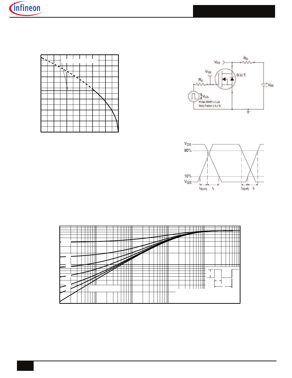
Fig. 2 Typical Output Characteristics
Fig. 3
Typical Transfer Characteristics
Fig. 4 Normalized On-Resistance
vs. Temperature
Fig. 1 Typical Output Characteristics
0.1
1
10
100
VDS, Drain-to-Source Voltage (V)
1
10
100
1000
I D
, D
ra
in
-t
o-
S
ou
rc
e
C
ur
re
nt
(
A
)
4.5V
20µs PULSE WIDTH
Tj = 25°C
VGS
TOP 15V
10V
8.0V
7.0V
6.0V
5.5V
5.0V
BOTTOM 4.5V
0.1
1
10
100
VDS, Drain-to-Source Voltage (V)
10
100
1000
I D
, D
ra
in
-t
o-
S
ou
rc
e
C
ur
re
nt
(
A
)
4.5V
20µs PULSE WIDTH
Tj = 175°C
VGS
TOP 15V
10V
8.0V
7.0V
6.0V
5.5V
5.0V
BOTTOM 4.5V
4.0
5.0
6.0
7.0
8.0
9.0
10.0
VGS, Gate-to-Source Voltage (V)
10
100
1000
I D
, D
ra
in
-t
o-
S
ou
rc
e
C
ur
re
nt
A
)
TJ = 25°C
TJ = 175°C
VDS = 25V
20µs PULSE WIDTH
-60
-40
-20
0
20
40
60
80
100 120 140 160 180
0.0
0.5
1.0
1.5
2.0
2.5
3.0
T , Junction Temperature
( C)
R
,
D
ra
in
-to
-S
ou
rc
e O
n R
es
is
ta
nc
e
(N
or
m
al
iz
ed
)
J
DS
(o
n
)
°
V
=
I
=
GS
D
10V
175A
AUIRF2805S/L
4
2015-9-30
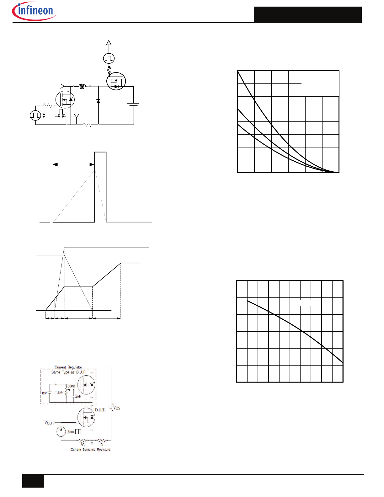
Fig 5. Typical Capacitance vs.
Drain-to-Source Voltage
Fig 6. Typical Gate Charge vs.
Gate-to-Source Voltage
Fig 8. Maximum Safe Operating Area
Fig. 7 Typical Source-to-Drain Diode
Forward Voltage
1
10
100
VDS, Drain-to-Source Voltage (V)
0
2000
4000
6000
8000
10000
C
, C
ap
ac
ita
nc
e
(p
F
)
Coss
Crss
Ciss
VGS = 0V, f = 1 MHZ
C iss = C gs + C gd , C ds
SHORTED
Crss = Cgd
Coss = Cds + Cgd
0
40
80
120
160
200
240
QG Total Gate Charge (nC)
0
4
8
12
16
20
V
G
S
, G
at
e-
to
-S
ou
rc
e
V
ol
ta
ge
(
V
)
VDS= 44V
VDS= 28V
ID= 104A
0.2 0.4 0.6 0.8 1.0 1.2 1.4 1.6 1.8
VSD, Source-toDrain Voltage (V)
0.1
1.0
10.0
100.0
1000.0
I S
D
, R
ev
er
se
D
ra
in
C
ur
re
nt
(A
)
TJ = 25°C
TJ = 175°C
VGS = 0V
1
10
100
1000
VDS , Drain-toSource Voltage (V)
1
10
100
1000
10000
I D
,
D
ra
in
-t
o-
S
ou
rc
e
C
ur
re
nt
(
A
)
Tc = 25°C
Tj = 175°C
Single Pulse
1msec
10msec
OPERATION IN THIS AREA
LIMITED BY RDS(on)
100µsec
AUIRF2805S/L
5
2015-9-30
Fig 10a. Switching Time Test Circuit
Fig 11. Maximum Effective Transient Thermal Impedance, Junction-to-Case
Fig 9. Maximum Drain Current vs. Case Temperature
25
50
75
100
125
150
175
0
20
40
60
80
100
120
140
T , Case Temperature
( C)
I
, Dr
ai
n
Cur
ren
t (
A
)
°
C
D
LIMITED BY PACKAGE
Fig 10b. Switching Time Waveforms
0.01
0.1
1
0.00001
0.0001
0.001
0.01
0.1
1
Notes:
1. Duty factor D =
t / t
2. Peak T
= P
x Z
+ T
1
2
J
DM
thJC
C
P
t
t
DM
1
2
t , Rectangular Pulse Duration (sec)
T
her
m
al
Res
pons
e
(Z
)
1
th
JC
0.01
0.02
0.05
0.10
0.20
D = 0.50
SINGLE PULSE
(THERMAL RESPONSE)
AUIRF2805S/L
6
2015-9-30
Fig 14.
Threshold Voltage vs. Temperature
Fig 12c. Maximum Avalanche Energy
vs. Drain Current
Fig 12a. Unclamped Inductive Test Circuit
Fig 12b. Unclamped Inductive Waveforms
R G
IAS
0.01
tp
D.U.T
L
VDS
+
- VDD
DRIVER
A
15V
20V
tp
V
(BR)DSS
I
AS
Fig 13b. Gate Charge Test Circuit
Fig 13a. Gate Charge Waveform
Vds
Vgs
Id
Vgs(th)
Qgs1 Qgs2
Qgd
Qgodr
25
50
75
100
125
150
175
0
200
400
600
800
Starting T , Junction Temperature
( C)
E
,
S
ing
le P
ul
se A
val
anc
he
E
ner
gy
(
m
J)
J
AS
°
ID
TOP
BOTTOM
42.5A
73.5A
104A
-75 -50 -25
0
25
50
75 100 125 150 175
TJ , Temperature ( °C )
1.0
2.0
3.0
4.0
-V
G
S
(t
h)
G
at
e
th
re
sh
ol
d
V
ol
ta
ge
(
V
)
ID = 250µA
AUIRF2805S/L
7
2015-9-30
Fig 15. Typical Avalanche Current vs. Pulse width
Notes on Repetitive Avalanche Curves , Figures 15, 16:
(For further info, see AN-1005 at
www.infineon.com
)
1. Avalanche failures assumption:
Purely a thermal phenomenon and failure occurs at a temperature far in
excess of T
jmax
. This is validated for every part type.
2. Safe operation in Avalanche is allowed as long as T
jmax
is not exceeded.
3. Equation below based on circuit and waveforms shown in Figures 12a, 12b.
4. P
D (ave)
= Average power dissipation per single avalanche pulse.
5. BV = Rated breakdown voltage (1.3 factor accounts for voltage increase
during
avalanche).
6. I
av
= Allowable avalanche current.
7.
T
=
Allowable rise in junction temperature, not to exceed
T
jmax
(assumed as
25°C in Figure 15, 16).
t
av =
Average time in avalanche.
D = Duty cycle in avalanche = t
av
·f
Z
thJC
(D, t
av
) = Transient thermal resistance, see Figures 13)
P
D (ave)
= 1/2 ( 1.3·BV·I
av
) =
T/ Z
thJC
I
av
= 2
T/ [1.3·BV·Z
th
]
E
AS (AR)
= P
D (ave)
·t
av
Fig 16. Maximum Avalanche Energy
vs. Temperature
25
50
75
100
125
150
175
Starting TJ , Junction Temperature (°C)
0
100
200
300
400
E
A
R
,
A
va
la
nc
he
E
ne
rg
y
(m
J)
TOP Single Pulse
BOTTOM 10% Duty Cycle
ID = 104A
1.0E-07
1.0E-06
1.0E-05
1.0E-04
1.0E-03
1.0E-02
1.0E-01
tav (sec)
0.1
1
10
100
1000
10000
A
va
la
nc
he
C
ur
re
nt
(
A
)
0.05
Duty Cycle = Single Pulse
0.10
Allowed avalanche Current vs
avalanche pulsewidth, tav
assuming
Tj = 25°C due to
avalanche losses. Note: In no
case should Tj be allowed to
exceed Tjmax
0.01
AUIRF2805S/L
8
2015-9-30
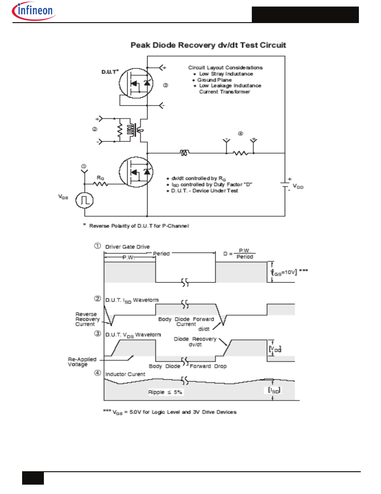
Fig 17. Peak Diode Recovery dv/dt Test Circuit for N-Channel HEXFET® Power MOSFETs
AUIRF2805S/L
9
2015-9-30
D
2
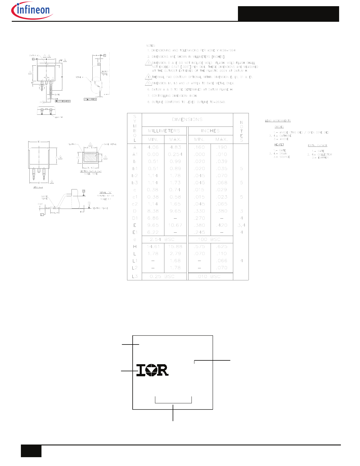
Pak (TO-263AB) Package Outline (Dimensions are shown in millimeters (inches))
YWWA
XX
XX
Date Code
Y= Year
WW= Work Week
AUF2805S
Lot Code
Part Number
IR Logo
D
2
Pak (TO-263AB) Part Marking Information
AUIRF2805S/L
10
2015-9-30
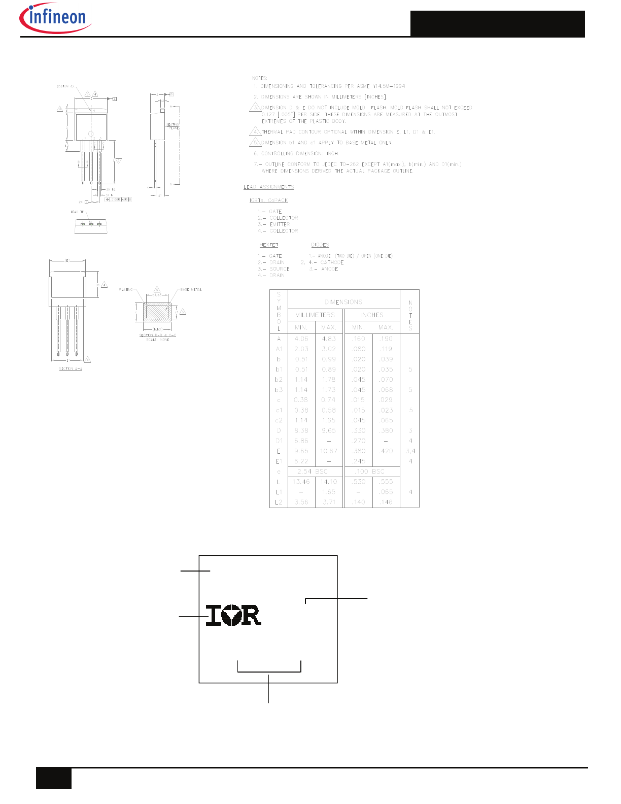
TO-262 Part Marking Information
YWWA
XX
XX
Date Code
Y= Year
WW= Work Week
AUF2805L
Lot Code
Part Number
IR Logo
TO-262 Package Outline (Dimensions are shown in millimeters (inches)