

Da t a S h e e t
V2.1 2013-10-22
CoolSET™ F3R80
ICE3AR4780VJZ
O f f - L i n e S M P S C u r r e n t M o d e C o n t r o l l e r wi t h
i n t e g r a t e d 8 0 0 V
CoolMOS™ and Startu p c ell
( i n p u t O V P & f r e q u e n c y j i t t e r ) i n D I P - 7
P o we r Ma n a g e m e n t & Mu lt im a r k e t

Edition 2013-10-22
Published by Infineon Technologies AG,
81726 Munich, Germany.
© 2013 Infineon Technologies AG
All Rights Reserved.
LEGAL DISCLAIMER
THE INFORMATION GIVEN IN THIS APPLICATION NOTE IS GIVEN AS A HINT FOR THE
IMPLEMENTATION OF THE INFINEON TECHNOLOGIES COMPONENT ONLY AND SHALL NOT BE
REGARDED AS ANY DESCRIPTION OR WARRANTY OF A CERTAIN FUNCTIONALITY, CONDITION OR
QUALITY OF THE INFINEON TECHNOLOGIES COMPONENT. THE RECIPIENT OF THIS APPLICATION
NOTE MUST VERIFY ANY FUNCTION DESCRIBED HEREIN IN THE REAL APPLICATION. INFINEON
TECHNOLOGIES HEREBY DISCLAIMS ANY AND ALL WARRANTIES AND LIABILITIES OF ANY KIND
(INCLUDING WITHOUT LIMITATION WARRANTIES OF NON-INFRINGEMENT OF INTELLECTUAL
PROPERTY RIGHTS OF ANY THIRD PARTY) WITH RESPECT TO ANY AND ALL INFORMATION GIVEN IN
THIS APPLICATION NOTE.
Information
For further information on technology, delivery terms and conditions and prices, please contact the nearest
Infineon Technologies Office (
www.infineon.com
).
Warnings
Due to technical requirements, components may contain dangerous substances. For information on the types in
question, please contact the nearest Infineon Technologies Office.
Infineon Technologies components may be used in life-support devices or systems only with the express written
approval of Infineon Technologies, if a failure of such components can reasonably be expected to cause the
failure of that life-support device or system or to affect the safety or effectiveness of that device or system. Life
support devices or systems are intended to be implanted in the human body or to support and/or maintain and
sustain and/or protect human life. If they fail, it is reasonable to assume that the health of the user or other
persons may be endangered.

CoolSET™ F3R80
ICE3AR4780VJZ
Data Sheet
3
V2.1, 2013-10-22
Trademarks of Infineon Technologies AG
AURIX™, C166™, CanPAK™, CIPOS™, CIPURSE™, EconoPACK™, CoolMOS™, CoolSET™,
CORECONTROL™, CROSSAVE™, DAVE™, DI-POL™, EasyPIM™, EconoBRIDGE™, EconoDUAL™,
EconoPIM™, EconoPACK™, EiceDRIVER™, eupec™, FCOS™, HITFET™, HybridPACK™, I²RF™,
ISOFACE™, IsoPACK™, MIPAQ™, ModSTACK™, my-d™, NovalithIC™, OptiMOS™, ORIGA™,
POWERCODE™; PRIMARION™, PrimePACK™, PrimeSTACK™, PRO-SIL™, PROFET™, RASIC™,
ReverSave™, SatRIC™, SIEGET™, SINDRION™, SIPMOS™, SmartLEWIS™, SOLID FLASH™,
TEMPFET™, thinQ!™, TRENCHSTOP™, TriCore™.
Other Trademarks
Advance Design Syst
em™ (ADS) of Agilent Technologies, AMBA™, ARM™, MULTI-ICE™, KEIL™,
PRIMECELL™, REALVIEW™, THUMB™, µVision™ of ARM Limited, UK. AUTOSAR™ is licensed by
AUTOSAR development partnership. Bluetooth™ of Bluetooth SIG Inc. CAT-iq™ of DECT Forum.
COLOSSUS™, FirstGPS™ of Trimble Navigation Ltd. EMV™ of EMVCo, LLC (Visa Holdings Inc.). EPCOS™
of Epcos AG. FLEXGO™ of Microsoft Corporation. FlexRay™ is licensed by FlexRay Consortium.
HYPERTERMINAL™ of Hilgraeve Incorporated. IEC™ of Commission Electrotechnique Internationale. IrDA™
of Infrared Data Association Corporation. ISO™ of INTERNATIONAL ORGANIZATION FOR
STANDARDIZATION. MATLAB™ of MathWorks, Inc. MAXIM™ of Maxim Integrated Products, Inc.
MICROTEC™, NUCLEUS™ of Mentor Graphics Corporation. MIPI™ of MIPI Alliance, Inc. MIPS™ of MIPS
Technologies, Inc., USA. muRata™ of MURATA MANUFACTURING CO., MICROWAVE OFFICE™ (MWO) of
Applied Wave Research Inc., OmniVision™ of OmniVision Technologies, Inc. Openwave™ Openwave Systems
Inc. RED HAT™ Red Hat, Inc. RFMD™ RF Micro Devices, Inc. SIRIUS™ of Sirius Satellite Radio Inc.
SOLARIS™ of Sun Microsystems, Inc. SPANSION™ of Spansion LLC Ltd. Symbian™ of Symbian Software
Limited. TAIYO
YUDEN™ of Taiyo Yuden Co. TEAKLITE™ of CEVA, Inc. TEKTRONIX™ of Tektronix Inc.
TOKO™ of TOKO KABUSHIKI KAISHA TA. UNIX™ of X/Open Company Limited. VERILOG™, PALLADIUM™
of Cadence Design Systems, Inc. VLYNQ™ of Texas Instruments Incorporated. VXWORKS™, WIND RIVER™
of WIND RIVER SYSTEMS, INC. ZETEX™ of Diodes Zetex Limited.
Last Trademarks Update 2011-11-11

CoolSET™ F3R80
ICE3AR4780VJZ
Data Sheet
4
V2.1, 2013-10-22
Revision History
Major changes since previous revision
Date
Version
Changed By
Change Description
22 Oct 2013
2.1
New datasheet format
We Listen to Your Comments
Is there any information in this document that you feel is wrong, unclear or missing?
Your
feedback
will
help
us
to
continuously
improve
the
quality
of
our
documentation.
Please send your proposal (including a reference to this document title/number) to:
ctdd@infineon.com

CoolSET™ F3R80
ICE3AR4780VJZ
Data Sheet
5
V2.1, 2013-10-22
Table of Contents
Revision History .............................................................................................................................................. 4
Table of Contents ............................................................................................................................................ 5
Off-
Line SMPS Current Mode Controller with integrated 800V CoolMOS™ and Startup cell (input OVP &
frequency jitter) in DIP-7 ................................................................................................................. 7
1
Pin Configuration and Functionality ........................................................................................... 8
1.1
Pin Configuration with PG-DIP-7 .................................................................................................... 8
1.2
Pin Functionality ............................................................................................................................. 8
2
Representative Block Diagram .................................................................................................. 10
3
Functional Description............................................................................................................... 11
3.1
Introduction .................................................................................................................................. 11
3.2
Power Management ..................................................................................................................... 11
3.3
Improved Current Mode ............................................................................................................... 12
3.3.1
PWM-OP................................................................................................................................. 14
3.3.2
PWM-Comparator ................................................................................................................... 14
3.4
Startup Phase .............................................................................................................................. 14
3.5
PWM Section ............................................................................................................................... 17
3.5.1
Oscillator ................................................................................................................................. 17
3.5.2
PWM-Latch FF1 ...................................................................................................................... 17
3.5.3
Gate Driver ............................................................................................................................. 17
3.6
Current Limiting ............................................................................................................................ 18
3.6.1
Leading Edge Blanking ........................................................................................................... 19
3.6.2
Propagation Delay Compensation (patented)........................................................................... 19
3.7
Control Unit .................................................................................................................................. 20
3.7.1
Basic and Extendable Blanking Mode ...................................................................................... 20
3.7.2
Active Burst Mode (patented) .................................................................................................. 21
3.7.2.1
Selectable burst entry level ................................................................................................. 22
3.7.2.2
Entering Active Burst Mode ................................................................................................ 23
3.7.2.3
Working in Active Burst Mode ............................................................................................. 23
3.7.2.4
Leaving Active Burst Mode ................................................................................................. 23
3.7.3
Protection Modes .................................................................................................................... 24
3.7.3.1
Vcc OVP, OTP and Vcc under voltage ................................................................................ 25
3.7.3.2
Over load, open loop protection .......................................................................................... 26
3.7.4
Input OVP Mode...................................................................................................................... 27
3.7.5
Action sequence at BV pin ...................................................................................................... 28
4
Electrical Characteristics ........................................................................................................... 30
4.1
Absolute Maximum Ratings .......................................................................................................... 30
4.2
Operating Range .......................................................................................................................... 31
4.3
Characteristics ............................................................................................................................. 31
4.3.1
Supply Section ........................................................................................................................ 31
4.3.2
Internal Voltage Reference ...................................................................................................... 32
4.3.3
PWM Section .......................................................................................................................... 32
4.3.4
Soft Start time ......................................................................................................................... 32
4.3.5
Control Unit ............................................................................................................................. 33
4.3.6
Current Limiting ....................................................................................................................... 34

CoolSET™ F3R80
ICE3AR4780VJZ
Data Sheet
6
V2.1, 2013-10-22
4.3.7
CoolMOS™ Section ................................................................................................................ 34
5
Typical Controller Performance Characteristics ...................................................................... 35
6
CoolMOS™ Performance Characteristics ................................................................................. 36
7
Input Power Curve ..................................................................................................................... 38
8
Outline Dimension ..................................................................................................................... 39
9
Marking ....................................................................................................................................... 40
10
Schematic for recommended PCB layout ................................................................................. 41
CoolSET™ F3R80
ICE3AR4780VJZ
Data Sheet
7
V2.1, 2013-10-22
Off-
Line SMPS Current Mode Controller with integrated 800V CoolMOS™
and Startup cell (input OVP & frequency jitter) in DIP-7
Product Highlights
800V avalanche rugged CoolMOS™ with startup cell
Active Burst Mode to reach the lowest Standby Power <100mW
Selectable entry and exit burst mode level
Adjustable blanking Window for high load jumps
Frequency jitter and soft driving for low EMI
Adjustable input OVP
Auto Restart protection for over load, over temperature and over voltage
Low Operating temperature down to -40°C
Pb-free lead plating, halogen free mold compound, RoHS compliant
Features
800V avalanche rugged CoolMOS™ with Startup Cell
Active Burst Mode for lowest Standby Power
Selectable entry and exit burst mode level
100kHz internally fixed switching frequency with jittering feature
Auto Restart Protection for Over load, Open Loop, VCC Under voltage & Over voltage and Over temperature
Over temperature protection with 50
°
C hysteresis
Built-in 10ms Soft Start
Built-in 20ms and extendable blanking time for short duration peak power
Propagation delay compensation for both maximum load and burst mode
Adjustable input OVP
Overall tolerance of Current Limiting < ±5%
BiCMOS technology for low power consumption and wide VCC voltage range
Soft gate drive with 50
Ω
turn on resistor
Description
The ICE3AR4780VJZ is a modified version of ICE3ARxx80JZ (CoolSET
™-F3R 800V) in DIP-7 package. It adds in
the input OVP feature but removes the brownout feature and external protection enable feature. In summary, the
ICE3AR4780VJZ is a device running at 100kHz, implemented with input OVP feature, installed with 800V MOSFET
with startup cell and housed in DIP-7 package. It provides good voltage margin of MOSFET, lowest standby power,
selectable burst level, reduced output ripple during burst mode, robust protection with input OVP feature, accurate
maximum power control for both maximum power and burst power, low EMI with frequency jittering and soft gate
drive, built-in and flexible protections, etc.
Applications
Adapter/Charger
Blue Ray/DVD player, Set-top Box, Digital Photo Frame
Auxiliary power supply for Server, PC, Printer, TV, Home theater/Audio System, White Goods, etc
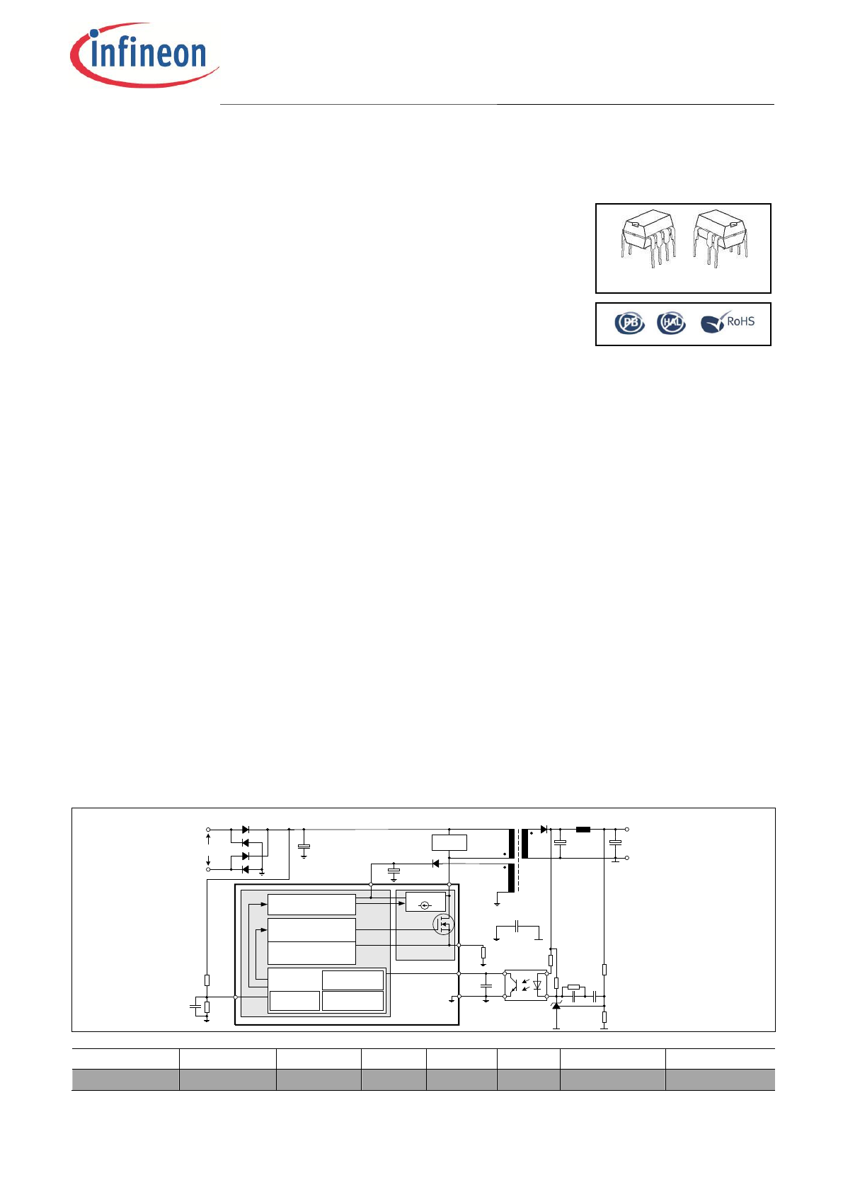
C
VCC
C
Bulk
Converter
DC Output
+
Snubber
Power Management
PWM Controller
Current Mode
85 ... 270 VAC
Typical Application
R
Sense
FBB
Control Unit
-
CS
VCC
Startup Cell
Precise Low Tolerance Peak
Current Limitation
Drain
CoolSET
®
- F3R80
(Input OVP & Jitter)
CoolMOS
®
GND
R
OV2
R
OV1
Active Burst Mode
Auto Restart Mode
Input OVP mode
BV
Figure 1:
Pin configuration PG-DIP-7(top view)
Type
Package
Marking
V
DS
F
OSC
R
DSon
1)
230VAC ±15%
2)
85-265 VAC
2)
ICE3AR4780VJZ
PG-DIP-7
3AR4780VJZ
800V
100kHz
4.7
7
31W
20W
1) typ @ T=25°C
2) Calculated maximum input power rating at T
a
=50°C, Ti=125°C and without copper area as heat sink.
PG-DIP7
CoolSET™ F3R80
ICE3AR4780VJZ
Pin Configuration and Functionality
Data Sheet
8
V2.1, 2013-10-22
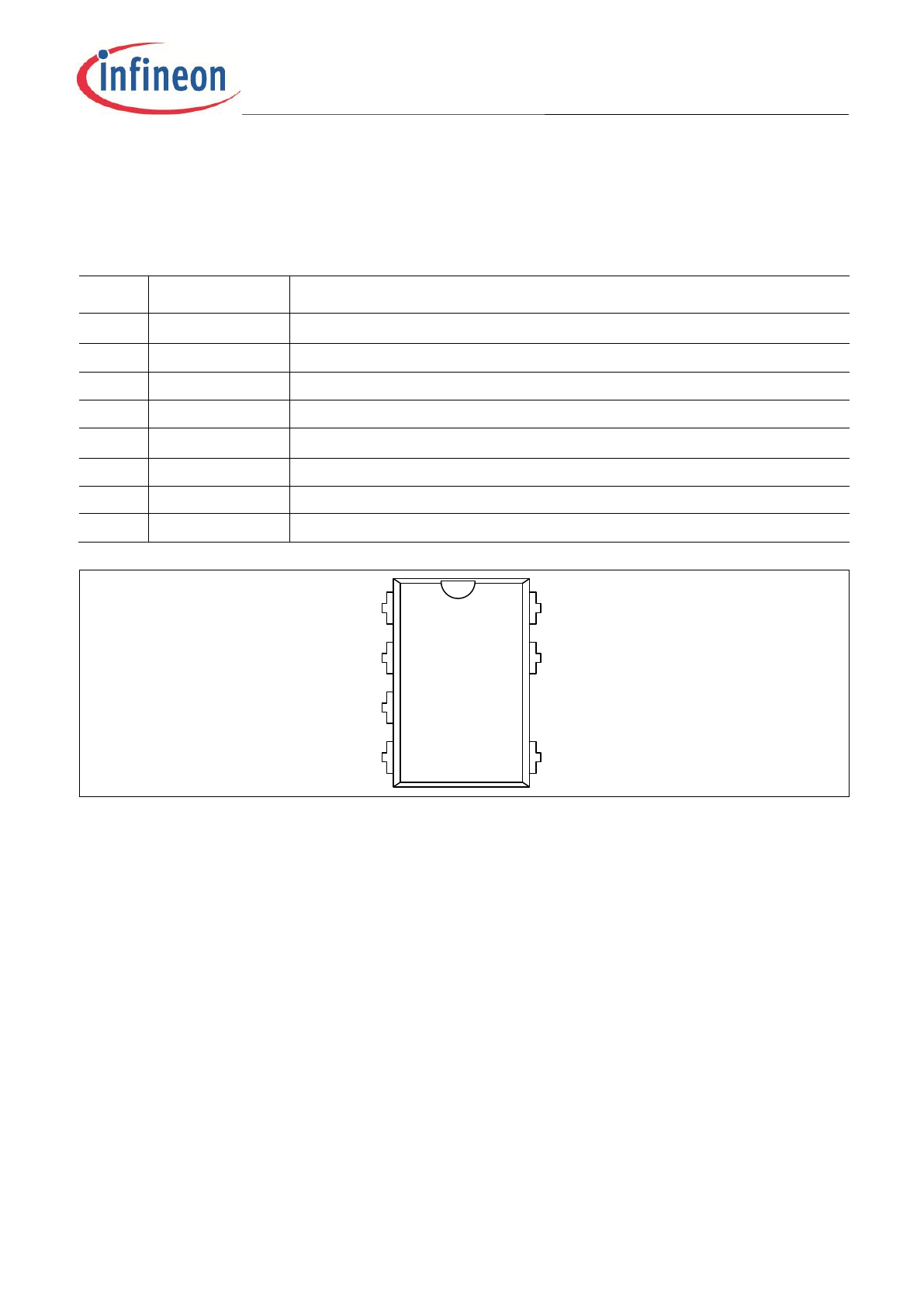
1
Pin Configuration and Functionality
1.1
Pin Configuration with PG-DIP-7
Pin
Symbol
Function
1
BV
extended Blanking time & input OVP
2
FBB
Feedback & Burst entry/exit control
3
CS
Current Sense/ 800V
CoolMOS™ Source
4
n.c.
not connected
5
Drain
800V
CoolMOS™ Drain
6
-
(no pin)
7
VCC
Controller Supply Voltage
8
GND
Controller Ground
1
7
8
4
3
2
5
GND
BV
FBB
CS
VCC
n.c.
Drain
Figure 2:
Pin configuration PG-DIP-7(top view)
1.2
Pin Functionality
BV (extended Blanking time & input OVP)
The BV pin combines the functions of input OVP and extendable blanking time for over load protection. The input
OVP feature is to stop the switching pulse when the input line voltage is higher than the V
OVP_ref
after the resistor
divider (Refer to Figure 3). The extendable blanking time function is to extend the built-in 20 ms blanking time for
over load protection by adding an external capacitor to ground.
FBB (Feedback & Burst entry control)
The FBB pin combines the feedback function and the burst entry/exit control. The regulation information is
provided by the FBB pin to the internal Protection Unit and the internal PWM-Comparator to control the duty cycle.
The FBB-signal is the only control signal in case of light load at the Active Burst Mode. The burst entry/ exit control
provides an access to select the entry/exit burst mode level.
CS (Current Sense)
The Current Sense pin senses the voltage developed on the shunt resistor inserted in the source of the integrated
CoolMOS™. If CS reaches the internal threshold of the Current Limit Comparator, the Driver output is immediately
switched off. Furthermore the current information is provided for the PWM comparator to realize the Current Mode.

CoolSET™ F3R80
ICE3AR4780VJZ
Pin Configuration and Functionality
Data Sheet
9
V2.1, 2013-10-22
Drain (Drain of integrated CoolMOS™)
Pin Drain is the connection to the Drain of the integrated CoolMOS™.
VCC (Power Supply)
The VCC pin is the positive supply of the IC. The operating range is between 10.5V and 25V.
GND (Ground)
The GND pin is the ground of the controller.
CoolSET™ F3R80
ICE3AR4780VJZ
Representative Block Diagram
Data Sheet
10
V2.1, 2013-10-22
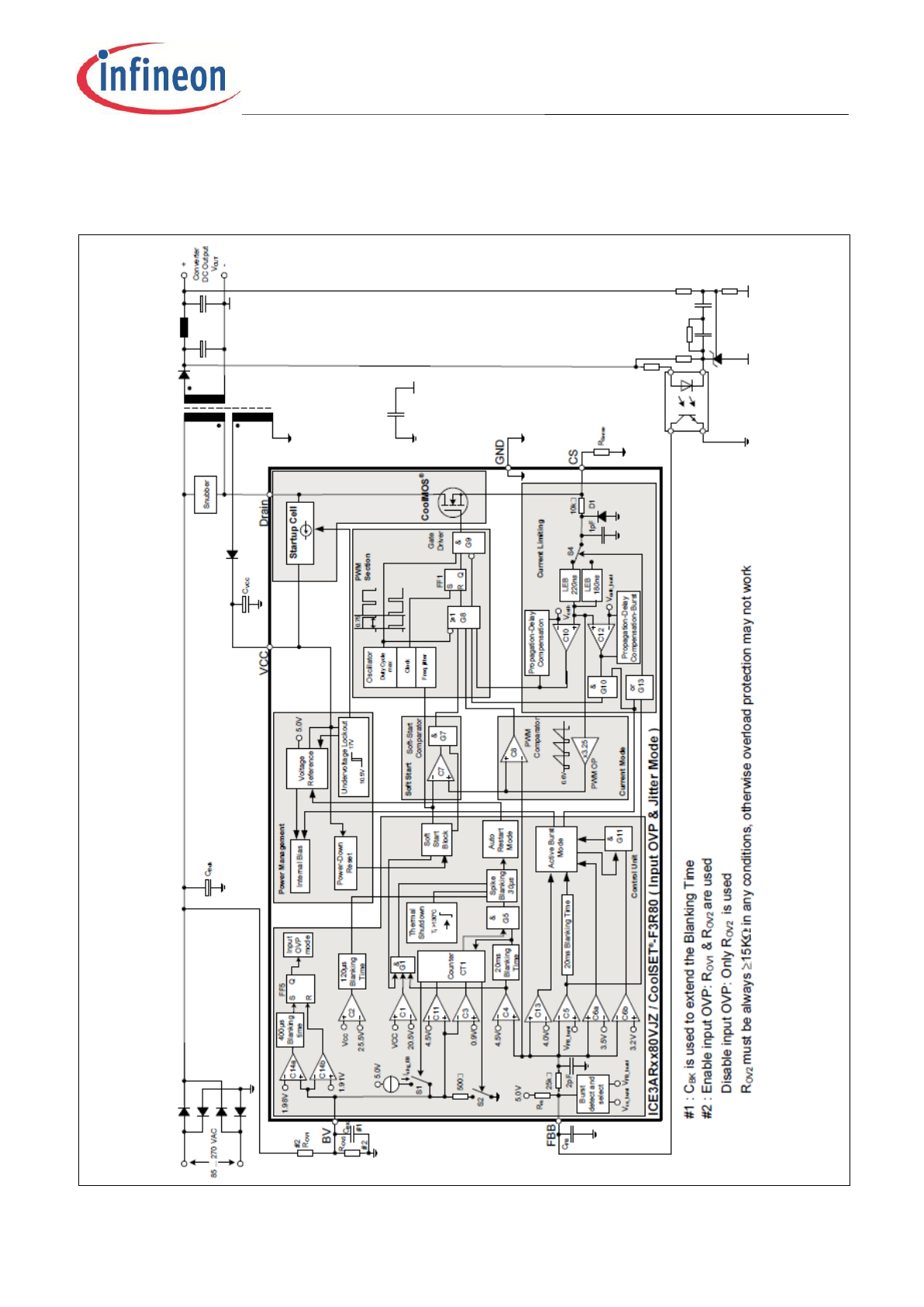
2
Representative Block Diagram
Figure 3:
Representative Block Diagram