
irf.com
© 2009 International Rectifier
October 11, 2010
Automotive Grade
AUIRS2336S
3-PHASE BRIDGE DRIVER IC
Features
• Drives up to six IGBT/MOSFET power devices
• Gate drive supplies up to 20 V per channel
• Over-current protection
• Over-temperature shutdown input
• Advanced input filter
• Integrated deadtime protection
• Shoot-through (cross-conduction) protection
• Undervoltage lockout for V
CC
& V
BS
• Enable/disable input and fault reporting
• Adjustable fault clear timing
• Separate logic and power grounds
• 3.3 V input logic compatible
* Qualification standards can be found on IR’s web site
www.
• Tolerant to negative transient voltage
• Designed for use with bootstrap power supplies
• Matched propagation delays for all channels
• -40°C to 125°C operating range
• RoHS
compliant
• Lead-Free
• Automotive
qualified*
Typical Applications
• HVAC
compressor
• Brushless automotive applications
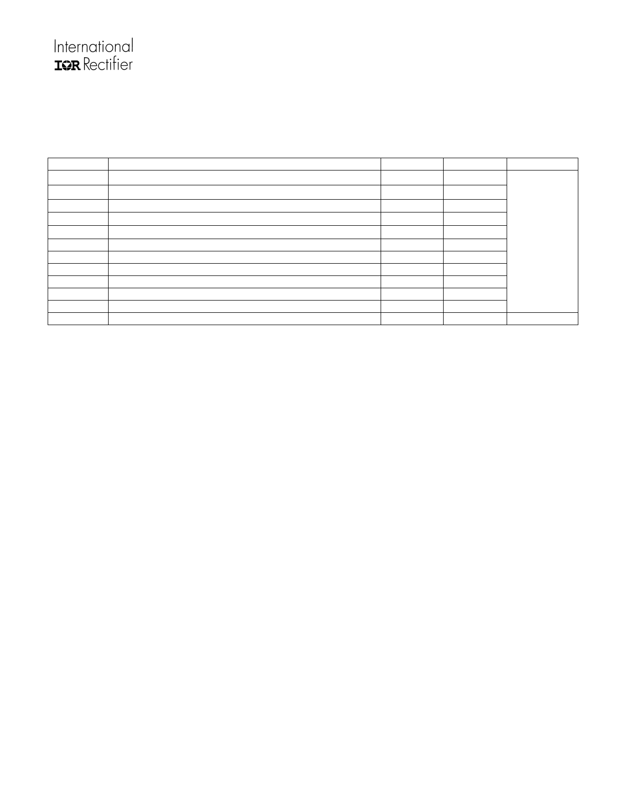
Product Summary
Topology 3
Phase
V
OFFSET
≤ 600 V
V
OUT
10 V – 20 V
I
o+
& I
o-
(typical)
200 mA & 350 mA
t
ON
& t
OFF
(typical)
530 ns & 530 ns
Deadtime (typical)
275 ns
Package Options
28-Lead SOIC Wide Body
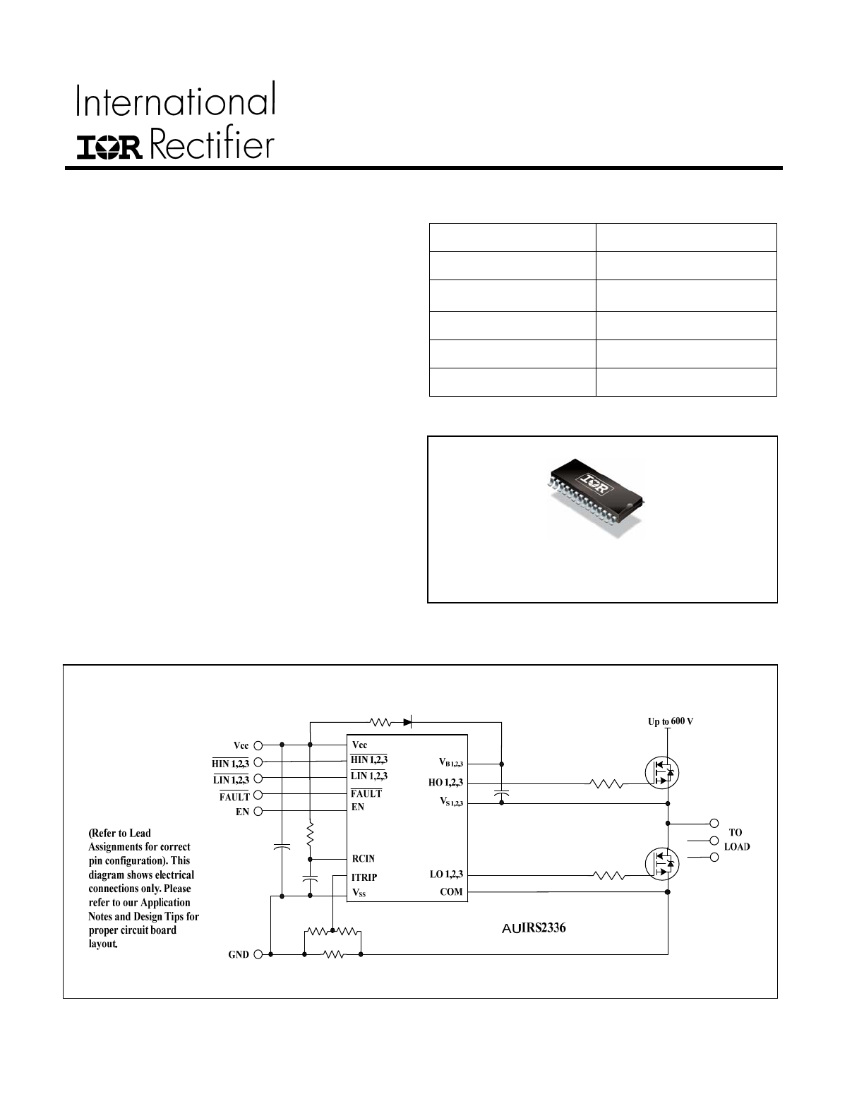
Typical Connection Diagram
AUIRS2336S
www.irf.com
© 2009 International Rectifier
2
Table of Contents
Page
Description
3
Qualification Information
4
Absolute Maximum Ratings
5
Recommended Operating Conditions
6
Static Electrical Characteristics
7-8
Dynamic Electrical Characteristics
9
Functional Block Diagram
10
Input/Output Pin Equivalent Circuit Diagram
11
Lead Definitions
12
Lead Assignments
13
Application Information and Additional Details
14-29
Parameter Temperature Trends
30-33
Package Details
34
Tape and Reel Details
35
Part Marking Information
36
Ordering Information
36

AUIRS2336S
www.irf.com
© 2009 International Rectifier
3
Description
The AUIRS2336S are high voltage, high speed, power MOSFET and IGBT gate drivers with three high-side and
three low-side referenced output channels for 3-phase applications. This IC is designed to be used with low-cost
bootstrap power supplies. Proprietary HVIC and latch immune CMOS technologies have been implemented in a
rugged monolithic structure. The floating logic input is compatible with standard CMOS or LSTTL outputs (down
to 3.3 V logic). A current trip function which terminates all six outputs can be derived from an external current
sense resistor. Enable functionality is available to terminate all six outputs simultaneously. An open-drain
FAULT signal is provided to indicate that a fault (e.g., over-current, over-temperature, or undervoltage shutdown
event) has occurred. Fault conditions are cleared automatically after a delay programmed externally via an RC
network connected to the RCIN input. The output drivers feature a high-pulse current buffer stage designed for
minimum driver cross-conduction. Shoot-through protection circuitry and a minimum deadtime circuitry have
been integrated into this IC. Propagation delays are matched to simplify the HVIC’s use in high frequency
applications. The floating channels can be used to drive N-channel power MOSFETs or IGBTs in the high-side
configuration, which operate up to 600 V.
AUIRS2336S
www.irf.com
© 2009 International Rectifier
4
Qualification Information
†
Automotive
(per AEC-Q100
††
)
Qualification Level
Comments: This family of ICs has passed an Automotive
qualification. IR’s Industrial and Consumer qualification
level is granted by extension of the higher Automotive level.
Moisture Sensitivity Level
MSL3
†††
260°C
(per IPC/JEDEC J-STD-020)
Machine Model
Class M2 (200V)
(per AEC-Q100-003)
Human Body Model
Class H1C (1500V)
(per AEC-Q100-002)
ESD
Charged Device Model
Class C4 (1000V)
(per AEC-Q100-011)
IC Latch-Up Test
Class II Level A
(per AEC-Q100-004)
RoHS Compliant
Yes
†
Qualification standards can be found at International Rectifier’s web site
http://www.irf.com/
††
Exceptions to AEC-Q100 requirements are noted in the qualification report.
††† Higher MSL ratings may be available for the specific package types listed here. Please contact your
International Rectifier sales representative for further information.
AUIRS2336S
www.irf.com
© 2009 International Rectifier
5
Absolute Maximum Ratings
Absolute maximum ratings indicate sustained limits beyond which damage to the device may occur. These are
stress ratings only, functional operation of the device at these or any other condition beyond those indicated in the
“Recommended Operating Condition” is not implied. Exposure to absolute maximum-rated conditions for extended
periods may affect device reliability. All voltage parameters are absolute voltages referenced to V
SS
unless otherwise
stated in the table. The thermal resistance and power dissipation ratings are measured under board mounted and
still air conditions. Voltage clamps are included between V
CC
& COM (25 V), V
CC
& V
SS
(20 V), and V
B
& V
S
(20 V).
Symbol Definition
Min
Max
Units
V
CC
Low side supply voltage
-0.3
20
†
V
IN
Logic input voltage (HIN, LIN, ITRIP, EN)
V
SS
-0.3 V
SS
+5.2
V
RCIN
RCIN input voltage
V
SS
-0.3 V
CC
+0.3
V
B
High-side floating well supply voltage
-0.3
620
†
V
S
High-side floating well supply return voltage
V
B
-20
†
V
B
+0.3
V
HO
Floating gate drive output voltage
V
S
-0.3 V
B
+0.3
V
LO
Low-side output voltage
COM-0.3
V
CC
+0.3
V
FLT
Fault output voltage
V
SS
-0.3 V
CC
+0.3
COM Power
ground
V
CC
-25 V
CC
+0.3
V
dV
S
/dt Allowable
V
S
offset supply transient relative to V
SS
—
50 V/ns
PW
HIN
High-side input pulse width
500
—
ns
P
D
Package power dissipation @ T
A
≤+25ºC
—
1.6 W
Rth
JA
Thermal resistance, junction to ambient
—
78 ºC/W
T
J
Junction temperature
—
150
T
S
Storage temperature
-55
150
T
L
Lead temperature (soldering, 10 seconds)
—
300
ºC
†
All supplies are tested at 25 V. An internal 20 V clamp exists for each supply.
AUIRS2336S
www.irf.com
© 2009 International Rectifier
6
Recommended Operating Conditions
For proper operation, the device should be used within the recommended conditions. All voltage parameters are
absolute voltages referenced to V
SS
unless otherwise stated in the table. The offset rating is tested with supplies of
(V
CC
-COM) = (V
B
-V
S
) = 15 V.
Symbol Definition
Min
Max
Units
V
CC
Low-side supply voltage
10
20
V
IN
HIN, LIN, & EN input voltage
V
SS
V
SS
+5
V
B
High-side floating well supply voltage
V
S
+10 V
S
+20
V
S
High-side floating well supply offset voltage
†
COM-8 600
V
S
(t)
Transient high-side floating supply voltage
††
-50 600
V
HO
Floating gate drive output voltage
V
s
V
B
V
LO
Low-side output voltage
COM
V
CC
COM Power
ground
-5
5
V
FLT
FAULT output voltage
V
SS
V
CC
V
RCIN
RCIN input voltage
V
SS
V
CC
V
ITRIP
ITRIP input voltage
V
SS
V
SS
+5
V
T
A
Ambient temperature
-40
125
ºC
† Logic operation for V
S
of –8 V to 600 V. Logic state held for V
S
of –8 V to –V
BS
.
†† Operational for transient negative V
S
of V
SS
- 50 V
with a 50 ns pulse width. Guaranteed by design. Refer to
the Application Information section of this datasheet for more details.
AUIRS2336S
www.irf.com
© 2009 International Rectifier
7
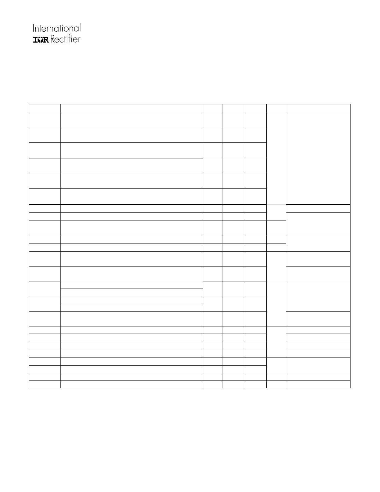
Static Electrical Characteristics
Unless otherwise noted, these specifications apply for an operating junction temperature range of -40°C ≤ Tj ≤ 125°C
with bias conditions of (V
CC
-COM) = (V
B
-V
S
) = 15 V. The V
IN
and I
IN
parameters are referenced to V
SS
and are
applicable to all six channels. The V
O
and I
O
parameters are referenced to respective V
S
and COM and are
applicable to the respective output leads HO or LO.
The V
CCUV
parameters are referenced to V
SS
. The V
BSUV
parameters are referenced to V
S
.
Symbol Definition Min
Typ
Max
Units
Test
Conditions
V
CCUV+
V
CC
supply undervoltage positive going threshold
8 8.9 9.8
V
CCUV-
V
CC
supply undervoltage negative going
threshold
7.4 8.2 9
V
CCUVHY
V
CC
supply undervoltage hysteresis
0.3 0.7 —
V
BSUV+
V
BS
supply undervoltage positive going threshold
8 8.9 9.8
V
BSUV-
V
BS
supply undervoltage negative going
threshold
7.4 8.2 9
V
BSUVHY
V
BS
supply undervoltage hysteresis
0.3 0.7 —
V NA
I
LK
High-side floating well offset supply leakage
— —
50 V
B
= V
S
= 600 V
I
QBS
Quiescent V
BS
supply current
—
70 120
µA
I
QCC
Quiescent V
CC
supply current
—
2 3
mA
All inputs are in the
off state
V
OH
High level output voltage drop, V
BIAS
-V
O
—
0.90 1.5 V
V
OL
Low level output voltage drop, V
O
—
0.40 0.6 V
I
O
= 20 mA
I
o+
Output high short circuit pulsed current
75
200
—
V
O
=0 V,V
IN
=0 V,
PW ≤ 10 µs
I
o-
Output low short circuit pulsed current
150
350
—
mA
V
O
=15 V,V
IN
=5 V,
PW ≤ 10 µs
Logic “0” input voltage
V
IH
Logic “1” input voltage
2.5
—
—
Logic “1” input voltage
V
IL
Logic “0” input voltage
—
—
0.8
NA
V
IN,CLAMP
Input voltage clamp
(HIN, LIN, ITRIP and EN)
4.8 5.2 5.65
V
I
IN
= 100 µA
I
HIN+
Input bias current (HO = High)
—
150 200
V
IN
= 0 V
I
HIN-
Input bias current (HO = Low)
— 110 150
V
IN
= 4 V
I
LIN+
Input bias current (LO = High)
— 150 200
V
IN
= 0 V
I
LIN-
Input bias current (LO = Low)
— 110 150
µA
V
IN
= 4 V
V
RCIN,TH
RCIN positive going threshold
—
8
—
V
RCIN,HY
RCIN
hysteresis
—
3
—
V
NA
I
RCIN
RCIN input bias current
— —
1 µA
V
RCIN
= 0 V or 15 V
R
ON,RCIN
RCIN low on resistance
—
50 100 Ω
I = 1.5 mA
AUIRS2336S
www.irf.com
© 2009 International Rectifier
8
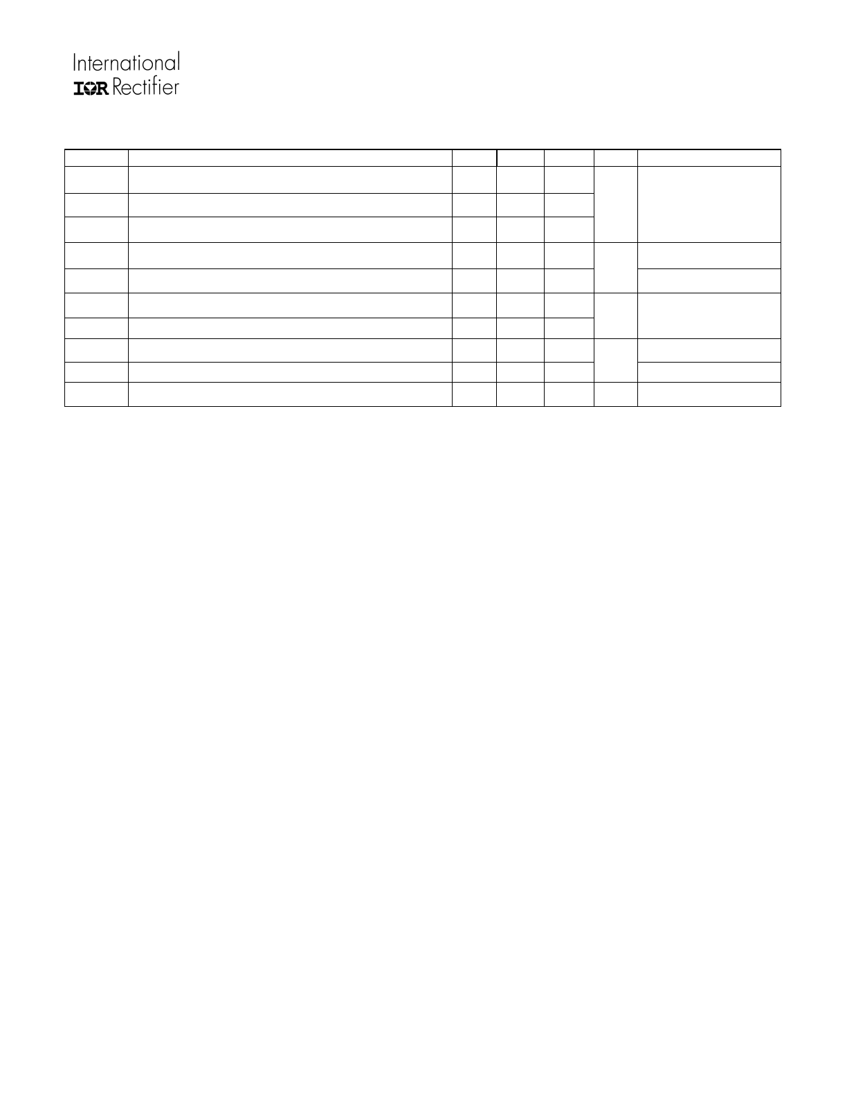
Static Electrical Characteristics (continued)
Symbol Definition Min
Typ
Max
Units
Test
Conditions
V
IT,TH+
ITRIP positive going threshold
0.37 0.46
0.55
V
IT,TH-
ITRIP negative going threshold
—
0.4
—
V
IT,HYS
ITRIP
hysteresis
—
0.07
—
V
NA
I
ITRIP+
“High” ITRIP input bias current
—
5 20
V
IN
= 4 V
I
ITRIP-
“Low” ITRIP input bias current
— — 1
µA
V
IN
= 0 V
V
EN,TH+
Enable positive going threshold
— — 2.5
V
EN,TH-
Enable negative going threshold
0.8
—
—
V
NA
I
EN+
“High” enable input bias current
—
5 20
V
IN
= 4 V
I
EN-
“Low” enable input bias current
— —
1
µA
V
IN
= 0 V
R
ON,FLT
FAULT low on resistance
—
50 100 Ω
I = 1.5 mA
AUIRS2336S
www.irf.com
© 2009 International Rectifier
9
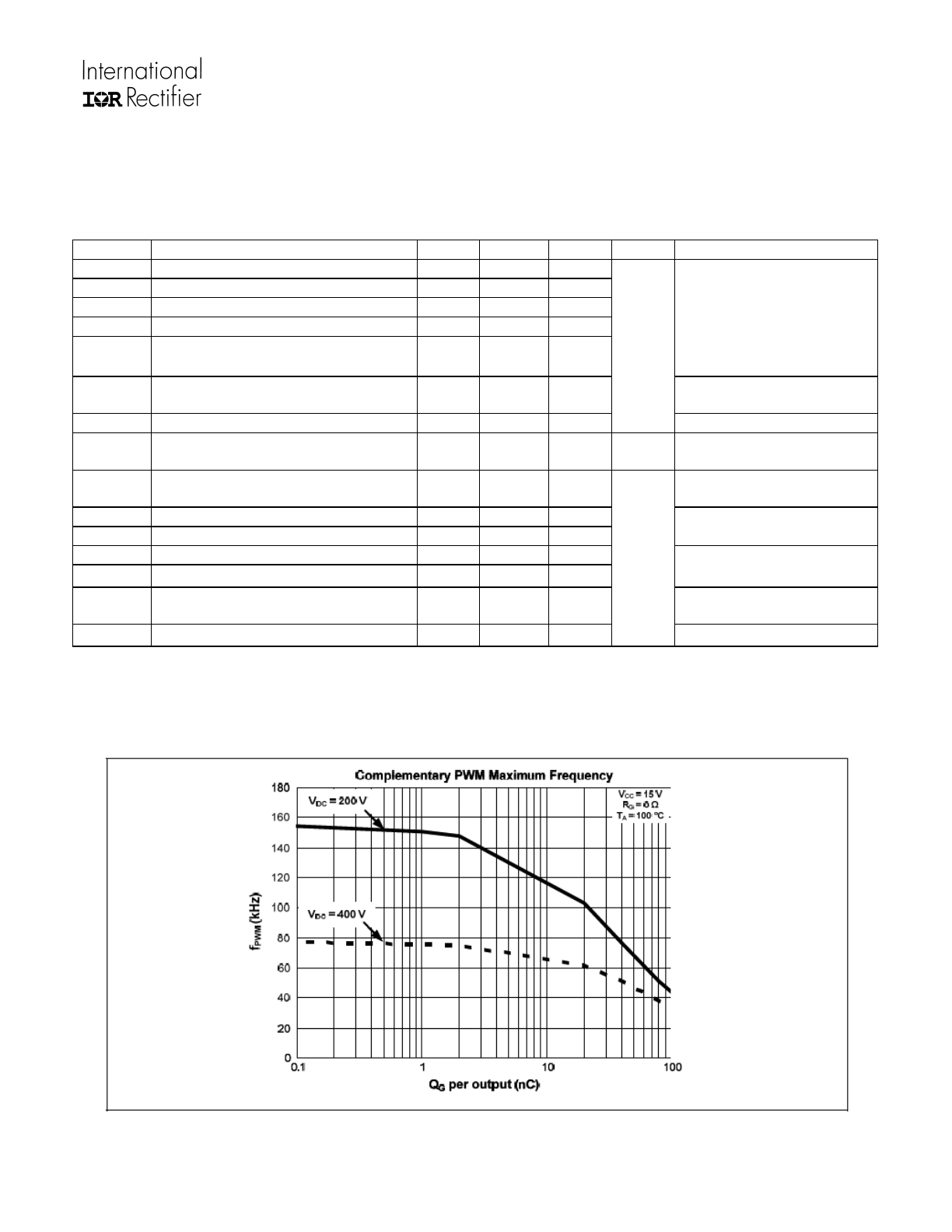
Dynamic Electrical Characteristics
Unless otherwise noted, these specifications apply for an operating junction temperature range of -40°C ≤ Tj ≤125°C
with bias conditions of V
CC
= V
B
= 15 V, V
S
= V
SS
= COM, T
A
= 25
o
C, and C
L
= 1000 pF. The dynamic electrical
characteristics are measured using the test definitions shown in Figure .
Symbol Definition Min
Typ
Max
Units
Test
Conditions
t
ON
Turn-on propagation delay
400
530
750
t
OFF
Turn-off propagation delay
400
530
750
t
R
Turn-on rise time
—
125 320
t
F
Turn-off fall time
—
50 120
t
FIL,IN
Input filter time
†
(HIN, LIN, ITRIP)
200 350 510
V
IN
= 0 V & 5 V
t
EN
Enable low to output shutdown
propagation delay
350 460 650
V
IN,
V
EN
= 0 V or 5 V
t
FILTER,EN
Enable input filter time
100
200
—
ns
NA
t
FLTCLR
FAULT clear time
RCIN: R = 2 MΩ, C = 1 nF
1 1.65 2.5 ms
V
IN
= 0 V or 5 V
V
ITRIP
= 0 V
t
ITRIP
ITRIP to output shutdown
propagation delay
500 750 1200
V
ITRIP
= 5 V
t
BL
ITRIP blanking time
—
400
—
t
FLT
ITRIP to FAULT propagation delay
400
600
950
V
IN
= 0 V or 5 V
V
ITRIP
= 5 V
DT Deadtime
190 275 420
MDT
DT matching
††
— —
100
V
IN
= 0 V & 5 V without
external deadtime
MT
Delay matching time (t
ON
, t
OFF
)
††
— — 50
V
IN
= 0 V & 5 V with external
deadtime larger than DT
PM
Pulse width distortion
†††
— —
100
ns
PW input=10 µs
†
The minimum width of the input pulse is recommended to exceed 500 ns to ensure the filtering time of the
input filter is exceeded.
†† This parameter applies to all of the channels. Please see the application section for more details.
††† PM is defined as PW
IN
- PW
OUT
.
AUIRS2336S
www.irf.com
© 2009 International Rectifier
10
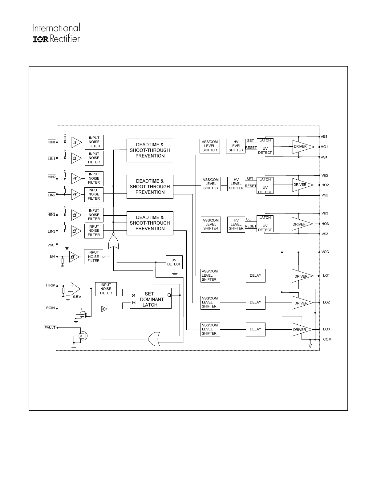
Functional Block Diagram:
AUIRS2336