
L292
SWITCH-MODE DRIVER FOR DC MOTORS
DRIVING CAPABILITY : 2 A, 36 V, 30 KHz
2 LOGIC CHIP ENABLE
EXTERNAL LOOP GAIN ADJUSTEMENT
SINGLE POWER SUPPLY (18 TO 36 V)
INPUT SIGNAL SYMMETRIC TO GROUND
THERMAL PROTECTION
DESCRIPTION
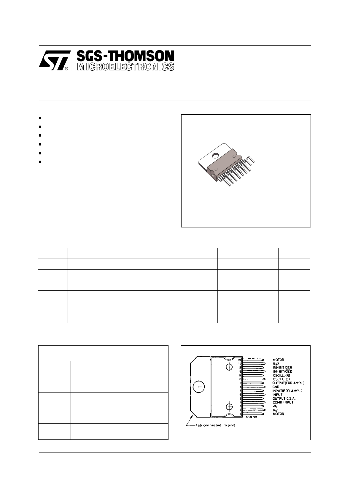
The L292 is a monolithic LSI circuit in 15-lead
Multiwatt ® package. It is intended for use, together
with L290 and L291, as a complete 3-chip motor
positioning system for applications such as car-
riage/daisy-wheel position control in type-writes.
The L290/1/2 system can be directly controlled by
a microprocessor.
March 1993
Symbol
Parameter
Value
Unit
V
s
Power Supply
36
V
V
i
Input Voltage
- 15 to + Vs
V
V
inhibit
Inhibit Voltage
0 to Vs
V
I
o
Output Current
2.5
A
P
tot
Total Power Dissipation (T
case
= 75
°
C)
25
W
T
stg
Storage and Junction Temperature
- 40 to + 150
°
C
ABSOLUTE MAXIMUM RATINGS
CONNECTION DIAGRAM (top view)
Vinhibit
Output Stage
Condition
Pin 12
Pin 13
L
L
Disabled
L
H
Normal Operation
H
L
Disabled
H
H
Disabled
TRUTH TABLE
ORDER CODE : L292
Multiwatt 15
1/12
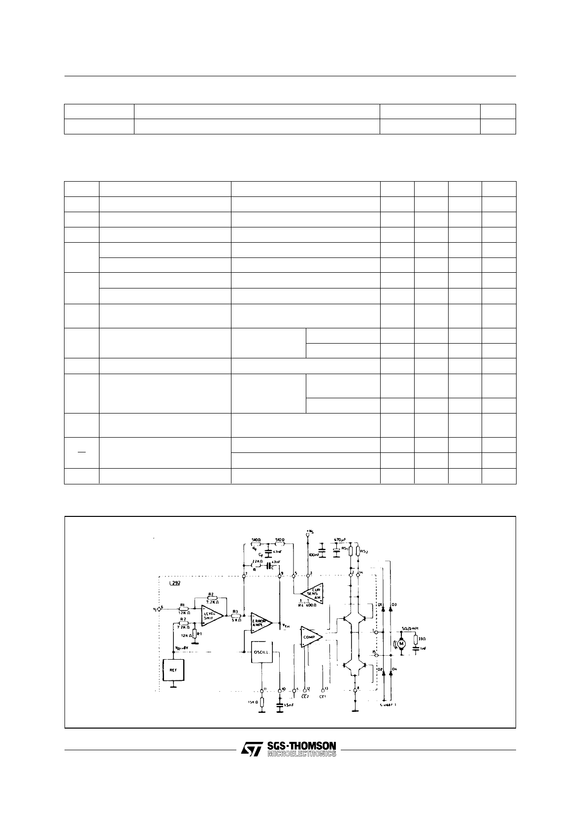
BLOCK DIAGRAM AND TEST CIRCUIT
Symbol
Parameter
Value
Unit
Rth-j-case
Thermal resistance junction-case
Max
3
°
C/W
THERMAL DATA
2/12
Symbol
Parameter
Test conditions
Min.
Typ.
Max.
Unit
V
s
Supply Voltage
18
36
V
I
d
Quiescent Drain Current
V
s
= 20 V (offset null)
30
50
mA
V
os
Input Offset Voltage (pin 6)
I
o
= 0
±
350
mV
V
inh
Inhibit Low Level (pin 12, 13)
2
V
Inhibit High Level (pin 12, 13)
3.2
V
I
inh
Low Voltage Condition
V
inh
(L) = 0.4 V
- 100
µ
A
High Voltage Conditions
V
inh
(H) = 3.2 V
10
µ
A
I
i
Input Current (pin 6)
V
l
= -8.8 V
V
l
= +8.8 V
-1.8
0.5
mA
mA
V
i
Input Voltage (pin 6)
R
s1
= R
s2
= 0.2
Ω
I
o
= 2A
9.1
V
I
o
= -2A
-9.1
V
I
o
Output Current
V
l
=
±
9.8 V R
s1
= R
s2
= 0.2
Ω
±
2
A
V
D
Total Drop Out Voltage
(inluding sensing
resistors)
I
o
= 2 A
5
V
I
o
= 1 A
3.5
V
V
RS
Sensing Rsistor Voltage
Drop
T
j
= 150
°
C
I
o
= 2 A
0.44
V
I
o
V
i
Transconductance
R
s1
= R
s2
=0.2
Ω
205
220
235
mA/V
R
s1
= R
s2
= 0.4
Ω
120
mA/V
f
osc
Frequency Range (pin 10)
1
30
KHz
ELECTRICAL CHARACTERISTICS (V
s
= 36 V, T
amb
= 25
°
C, f
osc
= 20 KHz unless otherwise specified)
L292
SYSTEM DESCRIPTION
The L290, L291 and L292 are intended to be used
as a 3-chip microprocessor controlled positioning
system. The device may be used separately - par-
ticularly the L292 motor driver - but since they will
usually be used together, a description of a typical
L290/1/2 system follows.
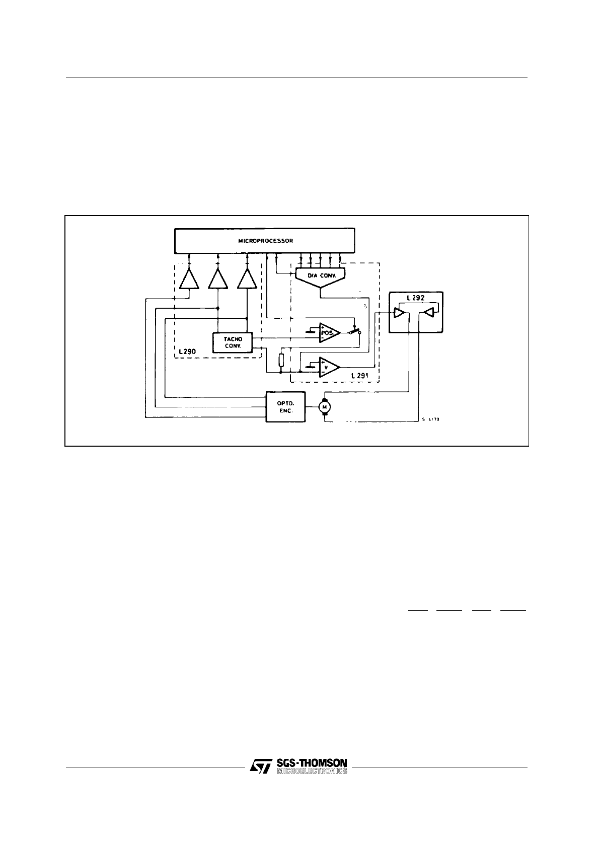
Figure 1. System Block Diagram
The system operates in two modes to achieve high
speed, high-accurancy positioning.
Speed commands for the system originate in the
microprocessor. It is continuosly updated on the
motor position by means of pulses from the L290
tachometer chip, whitch in tur gets its information
from the optical encoder. From this basic input, the
microprocessor computes a 5-bit control word that
sets the system speed dependent on the distance
to travel.
When the motor is stopped and the microprocessor
orders it to a new positio, the system operates
initially in an open-loop configuration as there is no
feedback from the tachometer generator. A maxi-
mum speed is reached, the tachometer chip output
backs off the processor signal thus reducing accel-
ering torque. The motor continues to run at rop
speed but under closed-loop control.
As the target position is approached, the microproc-
essor lowers the value of the speed-demand word;
this reduces the voltage at the main summing point,
in effect braking the motor. The braking is applied
progressively until the motor is running at minimum
speed.
At the time, the microprocessor orders a switch to
the position mode, (strobe signal at pin 8 of L291)
and within 3 to 4 ms the L292 drives the motor to
a null position, where it is held by electronic "de-
tenting".
The mechanical/electrical interface consists of an
optical encoder which generates two sinusoidal
signals 90
°
out of phase (leading according to the
motor direction) and proportional in frequency to the
speed of rotation. The optical encoder also provides
an output at one position on the disk which is used
to set the initial position.
The opto encoder signals, FTA and FTB are filtered
by the networks R
2
C
2
and R
3
C
3
(referring to Fig.4)
and are supplied to the FTA/FTB inputs on the L290.
The main function on the L290 is to implement the
following expression:
Output signal
(
TACHO
)
=
dV
AB
dt
•
FTA
|
FTA
|
−
dV
AA
dt
•
FTB
|
FTB
|
Thus the mean value of TACHO is proportional to
the rotation speed and its polarity indicates the
direction of rotation.
The above function is performed by amplifying the
input signals in A
1
and A
2
to obtain V
AA
and V
AB
(typ.7 V
p
). From V
AA
and V
AB
the external differen-
tiatior RC networks R
5
C
6
and R
4
C
4
give the signals
V
MA
and V
MB
which are fed to the multipliers.
3/12
L292

4/12
The second input to each multipler consists of the
sign of the first input of the other multiplier before
differentiation, these are obtained using the compa-
rators C
s1
and C
s2
. The multiplier outputs, C
SA
and
C
SB
, are summed by A
3
to give the final output
signal TACHO. The peak-topeak ripple signal of the
TACHO can be found from the following expression:
V
ripple
p
−
p
=
π
4
(
√
2
−
1
)
•
V
thaco
DC
The max value of TACHO is:
V
tacho
max
=
π
4
√
2
•
V
thaco
DC
Using the coparators C
1
and C
2
another two signals
from V
AA
and V
AB
are derived - the logic signals STA
and STB.
This signals are used by the microprocessor to
determine the position by counting the pulses.
The L2910 internal reference voltage is also derived
from V
AA
and V
AB
:
V
ref
=
|
V
AA
|
+
|
V
AB
|
This reference is used by the D/A converter in the
L291 to compensate for variations in input levels,
temperature changes and ageing.
The "one pulse per rotation" opto encoder output
is connected to pin 12 of the L290 (FTF) where it is
squared to give the STF logic output for the micro-
processor.
The TACHO signal and V
ref
are sent to the L291 via
filter networks R
8
C
8
R
9
and R
6
C
7
R
7
respectively.
Pin 12 of this chip is the main summing point of the
system where TACHO and the D/A converter output
are compared.
The input to D/A converter consists of 5 bit word
plus a sign bit supplied by the microprocessor. The
sign bit represets the direction of motor rotation.
The (analogue) output of the D/A conveter -
DAC/OUT - is compared with the TACHO signal and
the risulting error signal is amplified by the error
amplifier, and subsequently appears on pin 1.
The ERRV sognal (from pin 1 , L291) is fed to pin
6 of the final chip, the L292 H-bridge motor-driver.
This input signals is bidirectional so it must be
converted to a positive signal bacause the L292
uses a single supply voltage. This is accomplished
by the first stage - the level shifter, which uses an
internally generated 8 V reference.
This same reference voltage supplies the triangle
wave oscillator whose frequency is fixed by the
external RC network (R
20
, C
17
- pins 11 and 10)
where:
1 f
osc
=
1
2RC
(
with
R
≥
8.2
K
Ω
)
The oscillator determines the switching frequency
of the output stage and should be in the range 1 to
30 KHz.
Motor current is regulated by an internal loop in the
L292 which is performed by the resistors R
18
, R
19
and the differential current sense amplifier, the out-
put of which is filtered by an external RC network
and fed back to the error amplifier.
The choise of the external components in these RC
network (pins 5, 7, 9) is determined by the motor
type and the bandwidth requirements. The values
shown in the diagram are for a 5
Ω
, 5 MH motor.
(See L292 Transfer Function Calculation in Appli-
cation Information).
The error signal obtained by the addition of the input
and the current feedback signals (pin 7) is used to
pulse width modulate the oscillator signal by means
of the comparator. The pulse width modulated sig-
nal controls the duty cycle of the Hbridge to give an
output current corresponding to the L292 input
signal.
The interval between one side of the bridge switch-
ing off and the other switching on,
τ
, is programmed
by C
17
in conjuction with an internal resistor R
τ
.
This can be foud from:
τ
=
R
τ
•
C
pin
10.
(
C
17
in
the
diagram
)
Since R
τ
is approximately 1.5 K
Ω
and the recom-
mended
τ
to avoid simultaneous conduction is 2.5
µ
s C
pin 10
should be around 1.5 nF.
The current sense resistors R
18
and R
19
should be
high precision types (maximum tolerance
±
2 %)
and the recommended value is given by:
R
max
•
I
o
max
≤
0.44 V
It is possible to synchronize two L292 ’s, if desired,
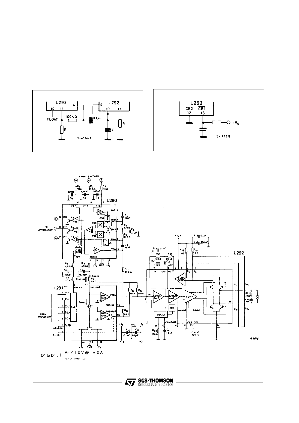
using the network shown in fig. 2.
Finally, two enable inputs are provited on the L292
(pins 12 and 13-active low and high respectively).
Thus the output stage may be inhibited by taking
pin 12 high or by taking pin 13 low. The output will
also be inhibited if the supply voltage falls below 18
V.
L292
The enable inputs were implemented in this way
because they are intended to be driven directly by
a microprocessor. Currently available microproces-
sors may generates spikes as high as 1.5 V during
power-up. These inputs may be used for a variety
of applications such as motor inhibit during reset of
the logical system and power-on reset (see fig. 3).
Figure 2.
Figure 3.
Figure 4 . Application Circuit.
5/12
L292
APPLICATION INFORMATION
This section has been added in order to help the designer for the best choise of the values of external
components.
Figure 5. L292 Block Diagram.
6/12
The schematic diagram used for the Laplace analysis of the system is shown in fig. 6.
Figure 6.
R
S1
= R
S2
= R
S
(sensing resistors)
1
R
4
= 2.5
•
10
-3
Ω
(current sensing amplifier transconductance)
L
M
= Motor inductance, R
M
= Motor resistance, I
M
= Motor current
G
mo
=
I
M
|
s
=
0 (DC transfer function from the input of the comparator (V
TH
) to the motor
current (I
M
)).
L292

Neglecting the VCEsat of the bridge transistors and the VBE of the diodes:
G
mo
=
1
R
M
2
V
s
V
R
where
: V
S
= supply voltage (1)
V
R
= 8 V (reference voltage)
DC TRANSFER FUNCTION
In order to be sure that the current loop is stable the following condition is imposed :
1 + sRC = 1 + s
L
M
R
M
(pole cancellation) (2)
from which RC =
L
M
R
M
(Note that in practice R must greater than 5.6 K
Ω
)
The transfer function is then,
I
M
V
I
(
s
)
=
R
2
R
4
R
1
R
3
G
mo
1
+
s R
F
C
F
G
mo
R
s
+
s R
4
C
+
s
2
R
F
C
F
R
4
C
(3)
In DC condition, this is reduced to
I
M
V
I
(
o
)
=
R
2
R
4
R
1
R
3
•
1
R
s
=
0.044
R
s
[
A
V
] (4)
OPEN-LOOP GAIN AND STABILITY CRITERION
For RC = L
M
/ R
M
, the open loop gain is:
A
β
=
1
sR subF C
•
G
mo
R
s
R
4
R
F
1
+
s
R
F
C
F
=
G
mo
R
s
R
4
C
1
s
(
1
+
s
R
F
C
F
)
(5)
In order to achieve good stability, the phase margin must be greater than 45
°
when | A
β
| = 1.
That means that, at f
F
=
1
2
π
R
F
C
F
must be | A
β
| < 1 (see fig. 7), that is :
| A
β
| f =
1
2
π
R
F
C
F
=
G
mo
R
s
R
4
C
R
F
C
F
√
2
<
1
(6)
Figure 7. Open Loop Frequency Response
7/12
L292
CLOSED-LOOP SYSTEM STEP RESPONSE
a) Small - signals analysis.
The transfer function (3) can be written as follows:
I
M
V
I
(
s
)
=
0.044
R
s
1
+
s
2
ξ
ω
o
1
+
2
ξ
s
+
s
2
ω
o
ω
o
2
(7)
where wo =
√
G
mo
R
s
R
4
C R
F
C
F
is the cutoff frequency
ξ
=
√
R
4
C
4 R
F
C
F
G
mo
R
s
is the dumping factor
By choosing the
ξ
value, it is possible to determine
the system response to an input step signal.
Examples :
1)
ξ
= 1 from which
I
M
(
t
)
=
0.044
R
s
[ 1
−
e
−
t
2R
F
C
F
(
1
+
t
4 R
F
C
F
)
]
•
V
i
(where Vi is the amplitude of the input step).
2)
ξ
=
1
√
2
from which
I
M
(
t
)
=
0.044
R
s
(
1
−
cos
t
2 R
F
C
F
e
−
t
2 R
F
C
F
)
V
i
Fi gure 8. Small S ignal Step Response
(normalized amplitude vs.
t / R
F
C
F
).
V
7
= 200 mV/div.
I
M
= 100 mA/div.
t = 100
µ
s/div.
with V
I
= 1.5 Vp.
8/12
L292

It is possible to verify that the L292 works in "closed-
loop" conditions during the entire motor current
rise-time: the voltage at pin 7 inverting input of the
error amplifier) is locked to the reference voltage
V
R
, present at the non-inverting input of the same
amplifier.
The previous linear analysis is correct for this ex-
ample.
Descresing the
ξ
value, the rise-time of the current
decreases. But for a good stability, from relationship
(6), the maximum value of
ξ
is:
CLOSED LOOP SYSTEM BANDWIDTH.
A good choice for x is the value 1 /
√
2. In this case :
I
M
V
I
(
s
)
=
0.044
R
s
1
+
s R
F
C
F
1
+
2s R
F
C
F
+
2s
2
R
F
2
C
F
2
The module of the transfer function is :
|
I
M
V
I
|
=
0.044
R
s
2
√
1
+
ω
2
R
F
2
C
F
2
√
[
(
1
+
2
ω
R
F
C
F
)
2
+
1
]
•
[
(
1
−
2
ω
R
F
C
F
)
2
+
1 ]
The cutoff frequency is derived by the expression (9) by putting |
I
M
V
I
|
=
0.707
•
0.044
R
s
(−
3 dB
)
, from
which :
ω
T
=
0.9
R
F
C
F
f
T
=
0.9
2
π
R
F
C
F
ξ
min
=
1
2
4
√
2
(phase margin = 45
°
)
b) Large signal reponse
The large step signal response is limited by slew-
rate and inductive load.
In this case, during the rise-time of the motor
current, The L292 works is open-loop condition.
(8)
(9)
9/12
L292

Example :
a) Data
- Motors characteristics:
LM = 5 mH
RM = 5 W
L
M
/ R
M
= 1msec
- Voltage and current characteristics:
V
s
= 20 V
I
M
= 2 A V
I
= 9.1 V
- Closed loop bandwidth : 3 kHz
b) Calculation
- From relationship (4) :
R
s
=
0.044
I
M
V
I
=
0.2
Ω
and from (1) :
G
mo
=
2V
S
R
M
V
R
=
1
Ω
−
1
- RC = 1 msec [from expression (2) ].
- Assuming
ξ
= 1/
√
2 ; from (7) follows :
ξ
2
=
1
2
=
400 C
4
R
F
C
F
•
0.2
- The cutoff frequency is :
f
T
=
143
•
10
−
3
R
F
C
F
=
3 kHz
c) Summarising
- RC = 1.10
-3
sec
-
1000 C
R
F
C
F
=
1
- R
F
C
F
≅
47
µ
s
C = 47 nF
R = 22 K
Ω
For R
F
= 510
Ω →
C
F
= 92 nF
10/12
L292
DIM.
mm
inch
MIN.
TYP.
MAX.
MIN.
TYP.
MAX.
A
5
0.197
B
2.65
0.104
C
1.6
0.063
D
1
0.039
E
0.49
0.55
0.019
0.022
F
0.66
0.75
0.026
0.030
G
1.02
1.27
1.52
0.040
0.050
0.060
G1
17.53
17.78
18.03
0.690
0.700
0.710
H1
19.6
0.772
H2
20.2
0.795
L
21.9
22.2
22.5
0.862
0.874
0.886
L1
21.7
22.1
22.5
0.854
0.870
0.886
L2
17.65
18.1
0.695
0.713
L3
17.25
17.5
17.75
0.679
0.689
0.699
L4
10.3
10.7
10.9
0.406
0.421
0.429
L7
2.65
2.9
0.104
0.114
M
4.25
4.55
4.85
0.167
0.179
0.191
M1
4.63
5.08
5.53
0.182
0.200
0.218
S
1.9
2.6
0.075
0.102
S1
1.9
2.6
0.075
0.102
Dia1
3.65
3.85
0.144
0.152
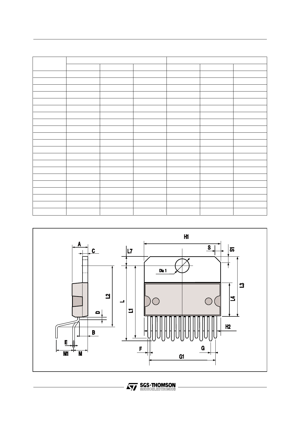
MULTIWATT15 PACKAGE MECHANICAL DATA
11/12
L292

12/12
Information furnished is believed to be accurate and reliable. However, SGS-THOMSON Microelectronics assumes no responsibility for the
consequences of use of such information nor for any infringement of patents or other rights of third parties which may result from its use. No
license is granted by implication or otherwise under any patent or patent rights of SGS-THOMSON Microelectronics. Specifications mentioned
in this publication are subject to change without notice. This publication supersedes and replaces all information previously supplied.
SGS-THOMSON Microelectronics products are not authorized for use as critical components in life support devices or systems without express
written approval of SGS-THOMSON Microelectronics.
© 1994 SGS-THOMSON Microelectronics - All Rights Reserved
SGS-THOMSON Microelectronics GROUP OF COMPANIES
Australia - Brazil - France - Germany - Hong Kong - Italy - Japan - Korea - Malaysia - Malta - Morocco - The Netherlands - Singapore -
Spain - Sweden - Switzerland - Taiwan - Thaliand - United Kingdom - U.S.A.
L292