
TL/H/7340
LM79XX
Series
3-Terminal
Negative
Regulators
November 1994
LM79XX Series 3-Terminal Negative Regulators
General Description
The LM79XX series of 3-terminal regulators is available with
fixed output voltages of
b
5V,
b
8V,
b
12V, and
b
15V.
These devices need only one external componentÐa com-
pensation capacitor at the output. The LM79XX series is
packaged in the TO-220 power package and is capable of
supplying 1.5A of output current.
These regulators employ internal current limiting safe area
protection and thermal shutdown for protection against vir-
tually all overload conditions.
Low ground pin current of the LM79XX series allows output
voltage to be easily boosted above the preset value with a
resistor divider. The low quiescent current drain of
these devices with a specified maximum change with line
and load ensures good regulation in the voltage boosted
mode.
For applications requiring other voltages, see LM137 data
sheet.
Features
Y
Thermal, short circuit and safe area protection
Y
High ripple rejection
Y
1.5A output current
Y
4% tolerance on preset output voltage
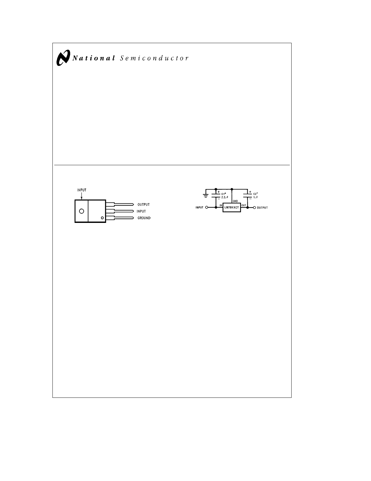
Connection Diagrams
TO-220 Package
TL/H/7340 – 14
Front View
Order Number LM7905CT, LM7912CT or LM7915CT
See NS Package Number TO3B
Typical Applications
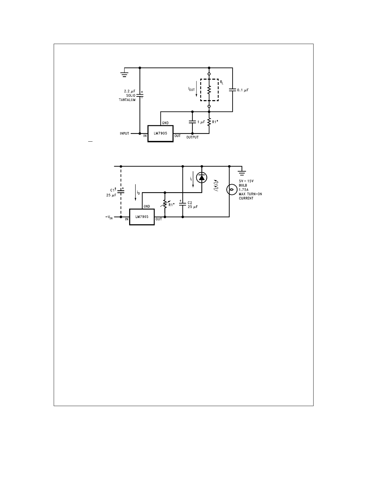
Fixed Regulator
TL/H/7340 – 3
*Required if regulator is separated from filter capacitor by
more than 3
×
. For value given, capacitor must be solid
tantalum. 25 mF aluminum electrolytic may be substituted.
²
Required for stability. For value given, capacitor must be
solid tantalum. 25 mF aluminum electrolytic may be substi-
tuted. Values given may be increased without limit.
For output capacitance in excess of 100 mF, a high current
diode from input to output (1N4001, etc.) will protect the
regulator from momentary input shorts.
C1995 National Semiconductor Corporation
RRD-B30M115/Printed in U. S. A.
Absolute Maximum Ratings
(Note 1)
If Military/Aerospace specified devices are required,
please contact the National Semiconductor Sales
Office/Distributors for availability and specifications.
Input Voltage
(V
o
e b
5V)
b
25V
(V
o
e b
12V and
b
15V)
b
35V
Input-Output Differential
(V
o
e b
5V)
25V
(V
o
e b
12V and
b
15V)
30V
Power Dissipation (Note 2)
Internally Limited
Operating Junction Temperature Range
0
§
C to
a
125
§
C
Storage Temperature Range
b
65
§
C to
a
150
§
C
Lead Temperature (Soldering, 10 sec.)
230
§
C
Electrical Characteristics
Conditions unless otherwise noted: I
OUT
e
500 mA, C
IN
e
2.2 mF, C
OUT
e
1 mF,
0
§
C
s
T
J
s
a
125
§
C, Power Dissipation
s
1.5W.
Part Number
LM7905C
Units
Output Voltage
b
5V
Input Voltage (unless otherwise specified)
b
10V
Symbol
Parameter
Conditions
Min
Typ
Max
V
O
Output Voltage
T
J
e
25
§
C
b
4.8
b
5.0
b
5.2
V
5 mA
s
I
OUT
s
1A,
b
4.75
b
5.25
V
P
s
15W
(
b
20
s
V
IN
s
b
7)
V
D
V
O
Line Regulation
T
J
e
25
§
C, (Note 3)
8
50
mV
(
b
25
s
V
IN
s
b
7)
V
2
15
mV
(
b
12
s
V
IN
s
b
8)
V
D
V
O
Load Regulation
T
J
e
25
§
C, (Note 3)
5 mA
s
I
OUT
s
1.5A
15
100
mV
250 mA
s
I
OUT
s
750 mA
5
50
mV
I
Q
Quiescent Current
T
J
e
25
§
C
1
2
mA
D
I
Q
Quiescent Current
With Line
0.5
mA
Change
(
b
25
s
V
IN
s
b
7)
V
With Load, 5 mA
s
I
OUT
s
1A
0.5
mA
V
n
Output Noise Voltage
T
A
e
25
§
C, 10 Hz
s
f
s
100 Hz
125
m
V
Ripple Rejection
f
e
120 Hz
54
66
dB
(
b
18
s
V
IN
s
b
8)
V
Dropout Voltage
T
J
e
25
§
C, I
OUT
e
1A
1.1
V
I
OMAX
Peak Output Current
T
J
e
25
§
C
2.2
A
Average Temperature
I
OUT
e
5 mA,
0.4
mV/
§
C
Coefficient of
0 C
s
T
J
s
100
§
C
Output Voltage
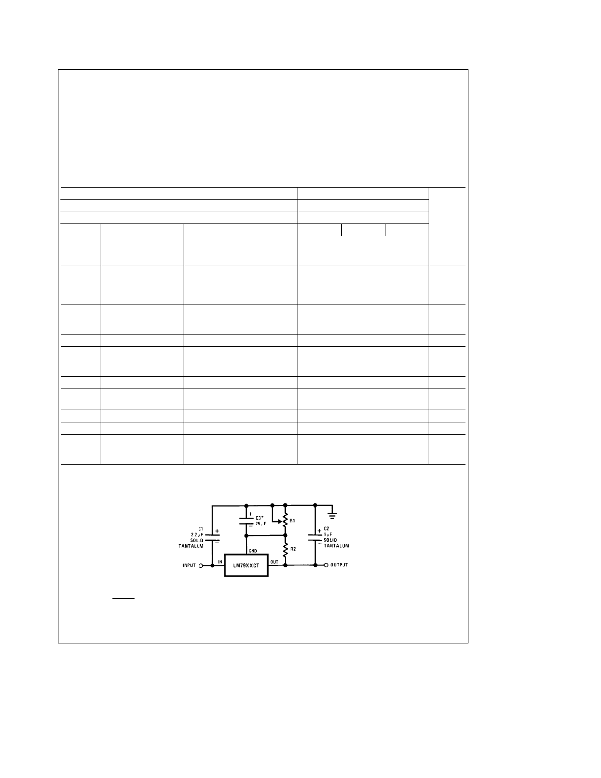
Typical Applications
(Continued)
Variable Output
TL/H/7340 – 2
*Improves transient response and ripple rejection. Do not increase beyond 50 mF.
V
OUT
e
V
SET
#
R1 a R2
R2
J
Select R2 as follows:
LM7905CT
300X
LM7912CT
750X
LM7915CT
1k
2
Electrical Characteristics
(Continued) Conditions unless otherwise noted: I
OUT
e
500 mA, C
IN
e
2.2 mF,
C
OUT
e
1 mF, 0
§
C
s
T
J
s
a
125
§
C, Power Dissipation
e
1.5W.
Part Number
LM7912C
LM7915C
Units
Output Voltage
b
12V
b
15V
Input Voltage (unless otherwise specified)
b
19V
b
23V
Symbol
Parameter
Conditions
Min
Typ
Max
Min
Typ
Max
V
O
Output Voltage
T
J
e
25
§
C
b
11.5
b
12.0
b
12.5
b
14.4
b
15.0
b
15.6
V
5 mA
s
I
OUT
s
1A,
b
11.4
b
12.6
b
14.25
b
15.75
V
P
s
15W
(
b
27
s
V
IN
s
b
14.5)
(
b
30
s
V
IN
s
b
17.5)
V
D
V
O
Line Regulation
T
J
e
25
§
C, (Note 3)
5
80
5
100
mV
(
b
30
s
V
IN
s
b
14.5)
(
b
30
s
V
IN
s
b
17.5)
V
3
30
3
50
mV
(
b
22
s
V
IN
s
b
16)
(
b
26
s
V
IN
s
b
20)
V
D
V
O
Load Regulation
T
J
e
25
§
C, (Note 3)
5 mA
s
I
OUT
s
1.5A
15
200
15
200
mV
250 mA
s
I
OUT
s
750 mA
5
75
5
75
mV
I
Q
Quiescent Current
T
J
e
25
§
C
1.5
3
1.5
3
mA
D
I
Q
Quiescent Current
With Line
0.5
0.5
mA
Change
(
b
30
s
V
IN
s
b
14.5)
(
b
30
s
V
IN
s
b
17.5)
V
With Load, 5 mA
s
I
OUT
s
1A
0.5
0.5
mA
V
n
Output Noise Voltage
T
A
e
25
§
C, 10 Hz
s
f
s
100 Hz
300
375
m
V
Ripple Rejection
f
e
120 Hz
54
70
54
70
dB
(
b
25
s
V
IN
s
b
15)
(
b
30
s
V
IN
s
b
17.5)
V
Dropout Voltage
T
J
e
25
§
C, I
OUT
e
1A
1.1
1.1
V
I
OMAX
Peak Output Current
T
J
e
25
§
C
2.2
2.2
A
Average Temperature
I
OUT
e
5 mA,
b
0.8
b
1.0
mV/
§
C
Coefficient of
0 C
s
T
J
s
100
§
C
Output Voltage
Note 1:
Absolute Maximum Ratings indicate limits beyond which damage to the device may occur. Operating Ratings indicate conditions for which the device is
intended to be functional, but do not guarantee Specific Performance limits. For guaranteed specifications and test conditions, see the Electrical Characteristics.
Note 2:
Refer to Typical Performance Characteristics and Design Considerations for details.
Note 3:
Regulation is measured at a constant junction temperature by pulse testing with a low duty cycle. Changes in output voltage due to heating effects must be
taken into account.
Typical Applications
(Continued)
Dual Trimmed Supply
TL/H/7340 – 4
3
Design Considerations
The LM79XX fixed voltage regulator series has thermal
overload protection from excessive power dissipation, inter-
nal short circuit protection which limits the circuit’s maxi-
mum current, and output transistor safe-area compensation
for reducing the output current as the voltage across the
pass transistor is increased.
Although the internal power dissipation is limited, the junc-
tion temperature must be kept below the maximum speci-
fied temperature (125
§
C) in order to meet data sheet specifi-
cations. To calculate the maximum junction temperature or
heat sink required, the following thermal resistance values
should be used:
Typ
Max
Typ
Max
Package
i
JC
i
JC
i
JA
i
JA
§
C/W
§
C/W
§
C/W
§
C/W
TO-220
3.0
5.0
60
40
P
D MAX
e
T
J Max
b
T
A
i
JC
a
i
CA
or
T
J Max
T
A
i
JA
i
CA
e
i
CS
a
i
SA
(without heat sink)
Solving for T
J
:
T
J
e
T
A
a
P
D
(i
JC
a
i
CA
) or
e
T
A
a
P
D
i
JA
(without heat sink)
Where:
T
J
e
Junction Temperature
T
A
e
Ambient Temperature
P
D
e
Power Dissipation
i
JA
e
Junction-to-Ambient Thermal Resistance
i
JC
e
Junction-to-Case Thermal Resistance
i
CA
e
Case-to-Ambient Thermal Resistance
i
CS
e
Case-to-Heat Sink Thermal Resistance
i
SA
e
Heat Sink-to-Ambient Thermal Resistance
Typical Applications
(Continued)
Bypass capacitors are necessary for stable operation of the
LM79XX series of regulators over the input voltage and out-
put current ranges. Output bypass capacitors will improve
the transient response by the regulator.
The bypass capacitors, (2.2 mF on the input, 1.0 mF on the
output) should be ceramic or solid tantalum which have
good high frequency characteristics. If aluminum electrolyt-
ics are used, their values should be 10 mF or larger. The
bypass capacitors should be mounted with the shortest
leads, and if possible, directly across the regulator termi-
nals.
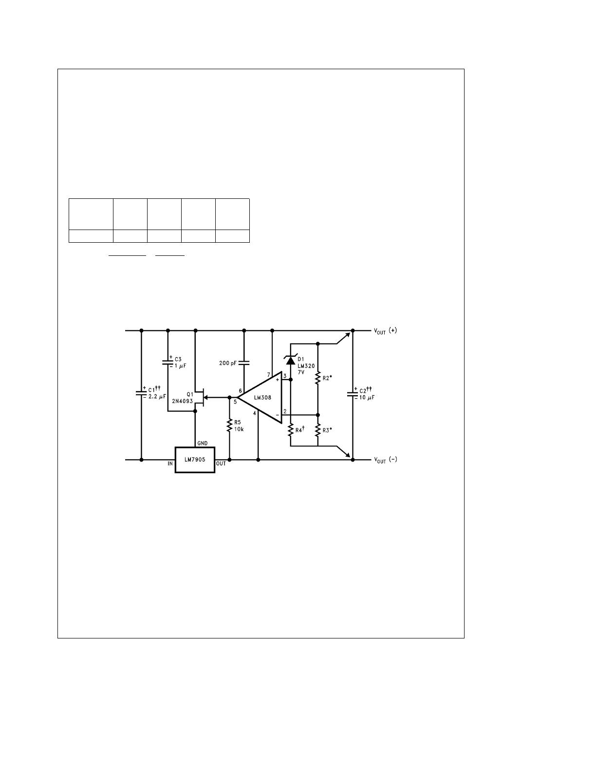
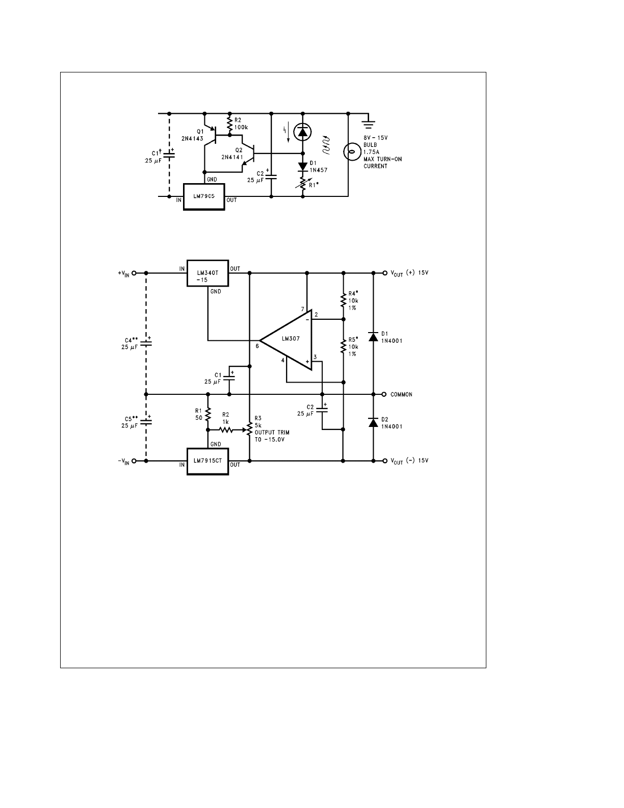
High Stability 1 Amp Regulator
TL/H/7340 – 5
Load and line regulation
k
0.01% temperature stability
s
0.2%
²Determine Zener current
²²Solid tantalum
*Select resistors to set output voltage. 2 ppm/
§
C tracking suggested
4
Typical Applications
(Continued)
Current Source
*I
OUT
e
1 mA a
5V
R1
TL/H/7340 – 7
Light Controller Using Silicon Photo Cell
TL/H/7340 – 8
*Lamp brightness increase until i
I
e
i
Q
(& 1 mA) a 5V/R1.
²Necessary only if raw supply filter capacitor is more than 2
×
from LM7905CT
5
Typical Applications
(Continued)
High-Sensitivity Light Controller
TL/H/7340 – 9
*Lamp brightness increases until i
i
e
5V/R1 (I
i
can be set as low as 1 mA)
²Necessary only if raw supply filter capacitor is more than 2
×
from LM7905
g
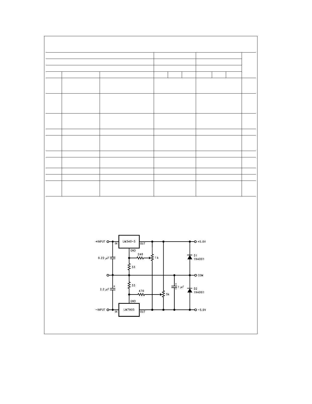
15V, 1 Amp Tracking Regulators
TL/H/7340 – 1
(b15)
(a15)
Load Regulation at DI
L
e
1A
40 mV
2 mV
Output Ripple, C
IN
e
3000 mF, I
L
e
1A
100 mVrms
100 mVrms
Temperature Stability
50 mV
50 mV
Output Noise 10 Hz
s
f
s
10 kHz
150 mVrms
150 mVrms
*Resistor tolerance of R4 and R5 determine matching of (a) and (b)
outputs.
**Necessary only if raw supply filter capacitors are more than 3
×
from regu-
lators.
6
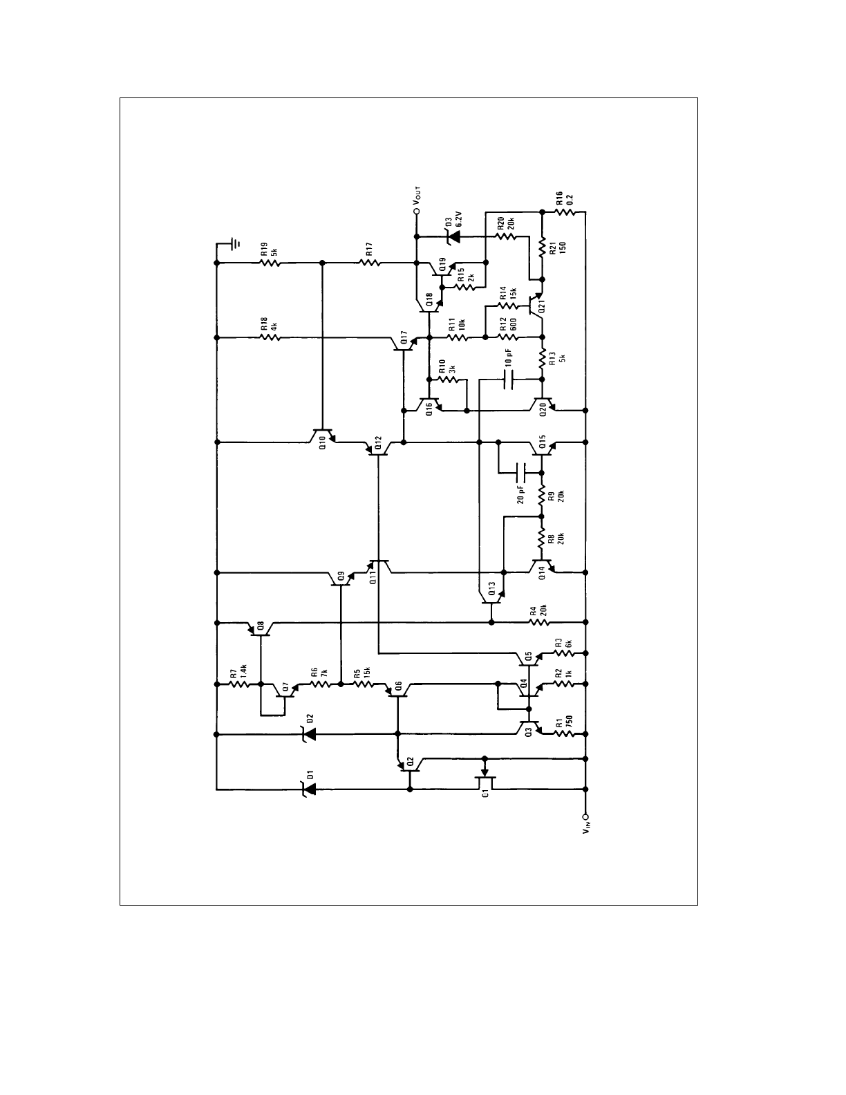
Schematic Diagrams
b
5V
TL/H/7340
–
1
2
7
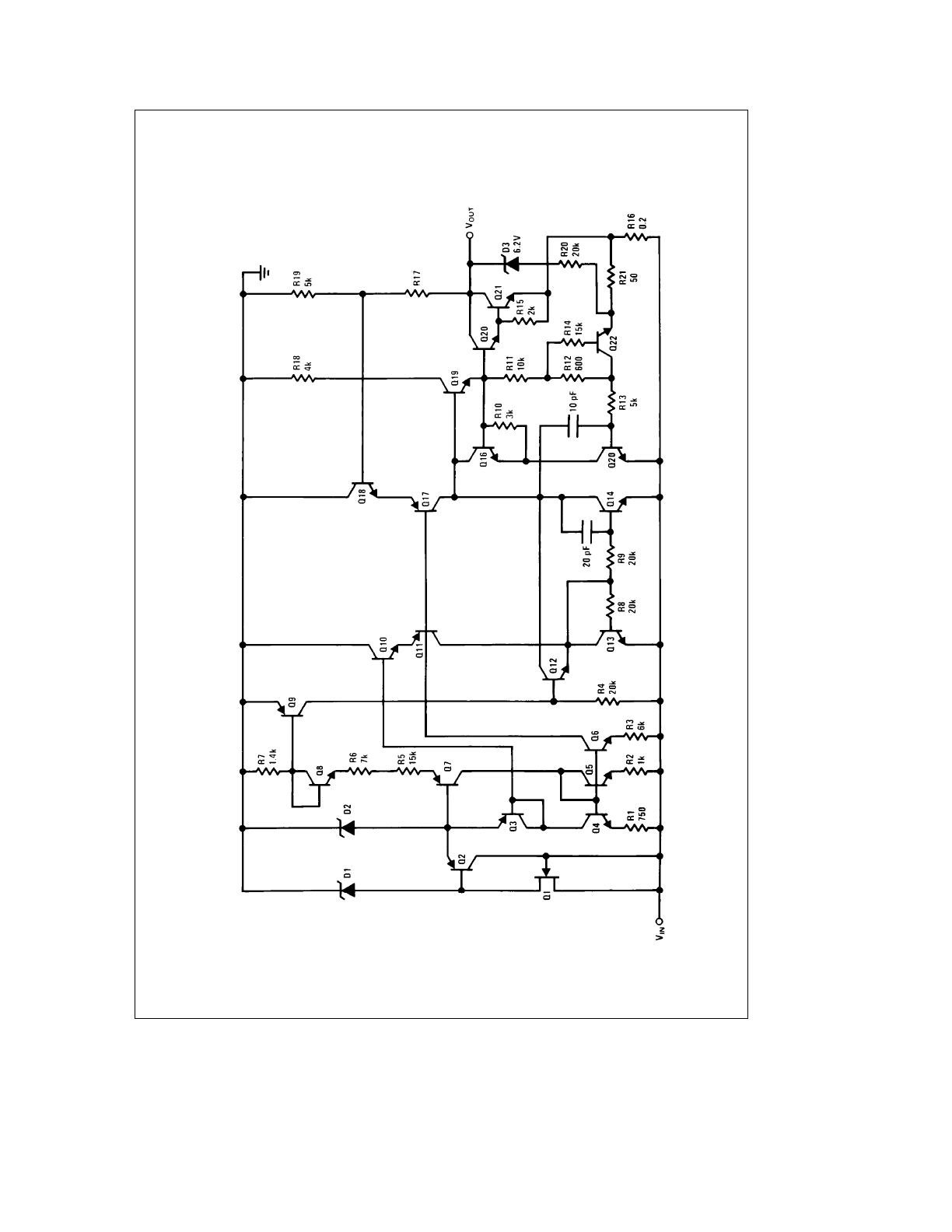
Schematic Diagrams
(Continued)
b
12V
and
b
15V
TL/H/7340
–
1
3
8

9
LM79XX
Series
3-Terminal
Negative
Regulators
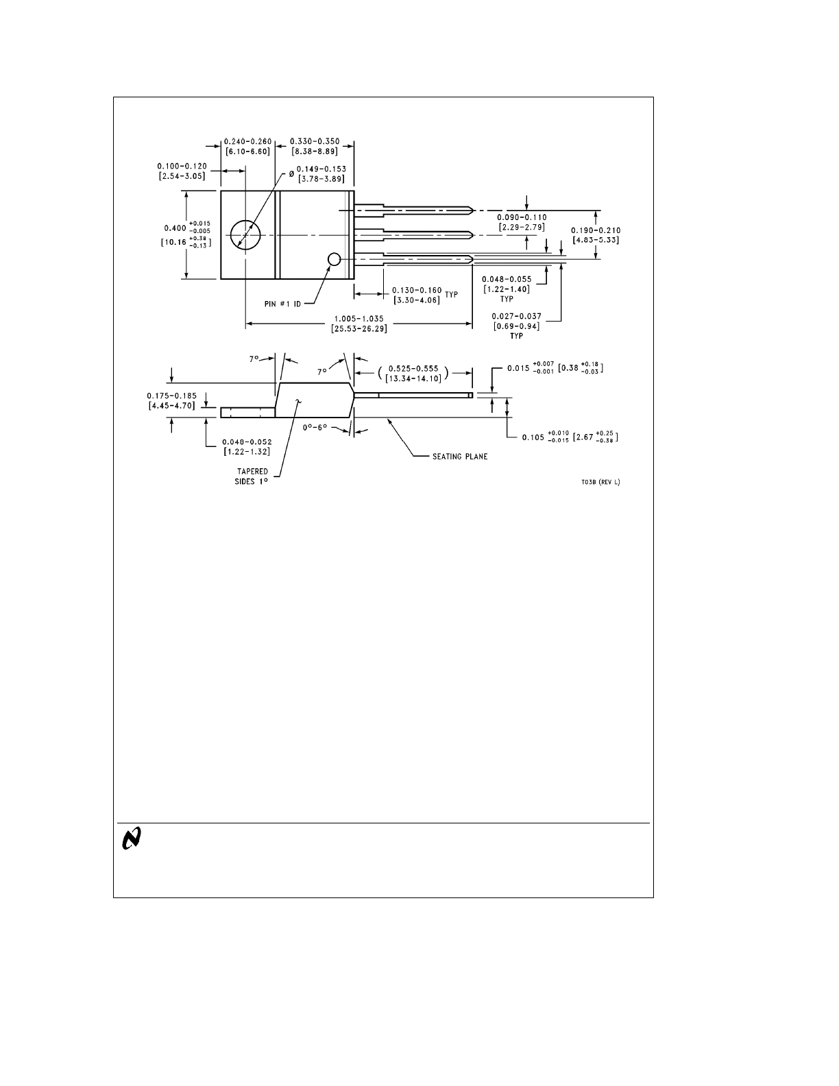
Physical Dimensions
inches (millimeters)
TO-220 Outline Package (T)
Order Number LM7905CT, LM7912CT or LM7915CT
NS Package Number T03B
LIFE SUPPORT POLICY
NATIONAL’S PRODUCTS ARE NOT AUTHORIZED FOR USE AS CRITICAL COMPONENTS IN LIFE SUPPORT
DEVICES OR SYSTEMS WITHOUT THE EXPRESS WRITTEN APPROVAL OF THE PRESIDENT OF NATIONAL
SEMICONDUCTOR CORPORATION. As used herein:
1. Life support devices or systems are devices or
2. A critical component is any component of a life
systems which, (a) are intended for surgical implant
support device or system whose failure to perform can
into the body, or (b) support or sustain life, and whose
be reasonably expected to cause the failure of the life
failure to perform, when properly used in accordance
support device or system, or to affect its safety or
with instructions for use provided in the labeling, can
effectiveness.
be reasonably expected to result in a significant injury
to the user.
National Semiconductor
National Semiconductor
National Semiconductor
National Semiconductor
Corporation
Europe
Hong Kong Ltd.
Japan Ltd.
1111 West Bardin Road
Fax: (
a
49) 0-180-530 85 86
13th Floor, Straight Block,
Tel: 81-043-299-2309
Arlington, TX 76017
Email: cnjwge
@
tevm2.nsc.com
Ocean Centre, 5 Canton Rd.
Fax: 81-043-299-2408
Tel: 1(800) 272-9959
Deutsch Tel: (
a
49) 0-180-530 85 85
Tsimshatsui, Kowloon
Fax: 1(800) 737-7018
English
Tel: (
a
49) 0-180-532 78 32
Hong Kong
Fran
3ais Tel: (
a
49) 0-180-532 93 58
Tel: (852) 2737-1600
Italiano
Tel: (
a
49) 0-180-534 16 80
Fax: (852) 2736-9960
National does not assume any responsibility for use of any circuitry described, no circuit patent licenses are implied and National reserves the right at any time without notice to change said circuitry and specifications.