
TL/F/8582
DP8390D/NS32490D
NIC
Network
Interface
Controller
July 1995
DP8390D/NS32490D NIC Network Interface Controller
General Description
The DP8390D/NS32490D Network Interface Controller
(NIC) is a microCMOS VLSI device designed to ease inter-
facing with CSMA/CD type local area networks including
Ethernet, Thin Ethernet (Cheapernet) and StarLAN. The
NIC implements all Media Access Control (MAC) layer func-
tions for transmission and reception of packets in accord-
ance with the IEEE 802.3 Standard. Unique dual DMA chan-
nels and an internal FIFO provide a simple yet efficient
packet management design. To minimize system parts
count and cost, all bus arbitration and memory support logic
are integrated into the NIC.
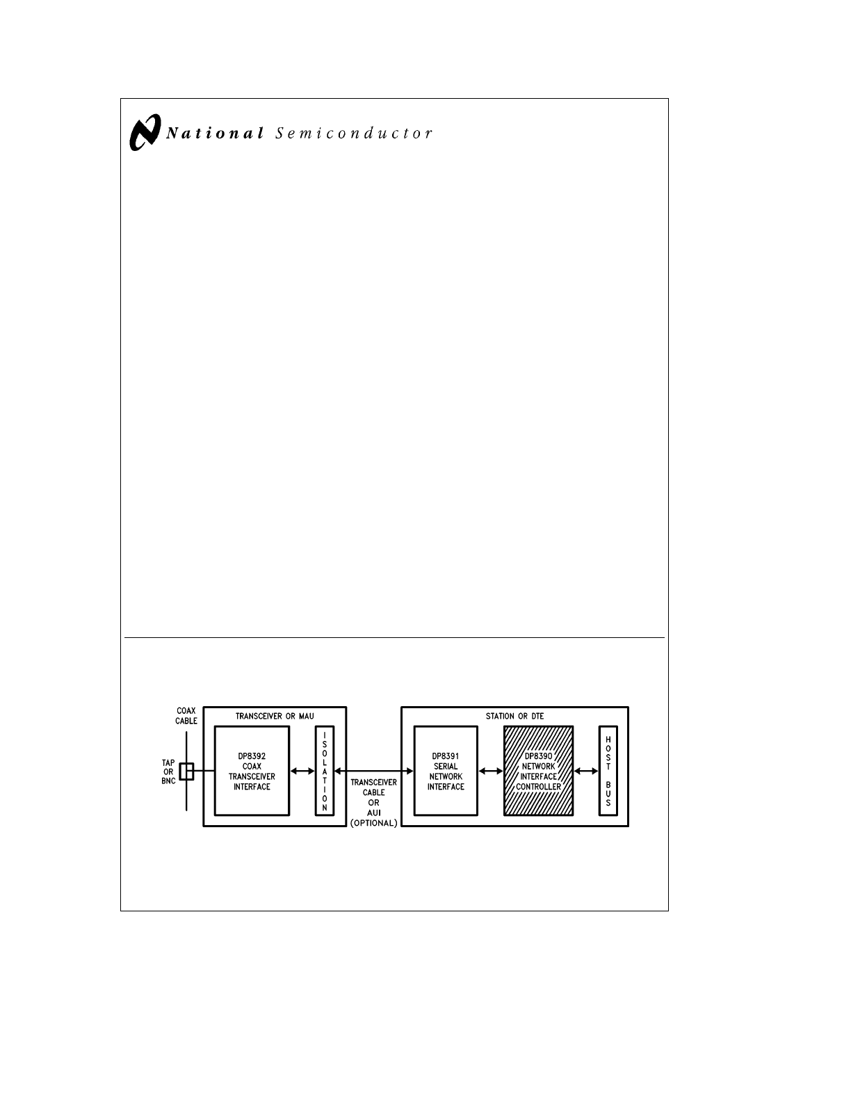
The NIC is the heart of a three chip set that implements the
complete IEEE 802.3 protocol and node electronics as
shown below. The others include the DP8391 Serial Net-
work Interface (SNI) and the DP8392 Coaxial Transceiver
Interface (CTI).
Features
Y
Compatible with IEEE 802.3/Ethernet II/Thin Ethernet/
StarLAN
Y
Interfaces with 8-, 16- and 32-bit microprocessor
systems
Y
Implements simple, versatile buffer management
Y
Requires single 5V supply
Y
Utilizes low power microCMOS process
Y
Includes
Ð Two 16-bit DMA channels
Ð 16-byte internal FIFO with programmable threshold
Ð Network statistics storage
Y
Supports physical, multicast, and broadcast address
filtering
Y
Provides 3 levels of loopback
Y
Utilizes independent system and network clocks
Table of Contents
1.0 SYSTEM DIAGRAM
2.0 BLOCK DIAGRAM
3.0 FUNCTIONAL DESCRIPTION
4.0 TRANSMIT/RECEIVE PACKET ENCAPSULATION/
DECAPSULATION
5.0 PIN DESCRIPTIONS
6.0 DIRECT MEMORY ACCESS CONTROL (DMA)
7.0 PACKET RECEPTION
8.0 PACKET TRANSMISSION
9.0 REMOTE DMA
10.0 INTERNAL REGISTERS
11.0 INITIALIZATION PROCEDURES
12.0 LOOPBACK DIAGNOSTICS
13.0 BUS ARBITRATION AND TIMING
14.0 PRELIMINARY ELECTRICAL CHARACTERISTICS
15.0 SWITCHING CHARACTERISTICS
16.0 PHYSICAL DIMENSIONS
1.0 System Diagram
IEEE 802.3 Compatible Ethernet/Thin Ethernet Local Area Network Chip Set
TL/F/8582 – 1
TRI-STATE
É
is a registered trademark of National Semiconductor Corporation.
C1995 National Semiconductor Corporation
RRD-B30M105/Printed in U. S. A.
2.0 Block Diagram
TL/F/8582 – 2
FIGURE 1
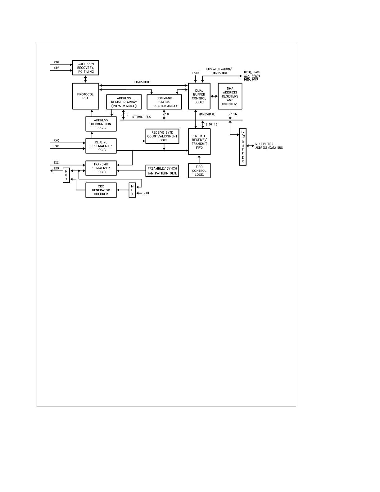
3.0 Functional Description
(Refer to
Figure 1
)
RECEIVE DESERIALIZER
The Receive Deserializer is activated when the input signal
Carrier Sense is asserted to allow incoming bits to be shift-
ed into the shift register by the receive clock. The serial
receive data is also routed to the CRC generator/checker.
The Receive Deserializer includes a synch detector which
detects the SFD (Start of Frame Delimiter) to establish
where byte boundaries within the serial bit stream are locat-
ed. After every eight receive clocks, the byte wide data is
transferred to the 16-byte FIFO and the Receive Byte Count
is incremented. The first six bytes after the SFD are
checked for valid comparison by the Address Recognition
Logic. If the Address Recognition Logic does not recognize
the packet, the FIFO is cleared.
CRC GENERATOR/CHECKER
During transmission, the CRC logic generates a local CRC
field for the transmitted bit sequence. The CRC encodes all
fields after the synch byte. The CRC is shifted out MSB first
following the last transmit byte. During reception the CRC
logic generates a CRC field from the incoming packet. This
local CRC is serially compared to the incoming CRC ap-
pended to the end of the packet by the transmitting node. If
the local and received CRC match, a specific pattern will be
generated and decoded to indicate no data errors. Trans-
mission errors result in a different pattern and are detected,
resulting in rejection of a packet.
TRANSMIT SERIALIZER
The Transmit Serializer reads parallel data from the FIFO
and serializes it for transmission. The serializer is clocked by
the transmit clock generated by the Serial Network Interface
(DP8391). The serial data is also shifted into the CRC gen-
erator/checker. At the beginning of each transmission, the
Preamble and Synch Generator append 62 bits of 1,0 pre-
amble and a 1,1 synch pattern. After the last data byte of
the packet has been serialized the 32-bit FCS field is shifted
directly out of the CRC generator. In the event of a collision
the Preamble and Synch generator is used to generate a
32-bit JAM pattern of all 1’s
ADDRESS RECOGNITION LOGIC
The address recognition logic compares the Destination Ad-
dress Field (first 6 bytes of the received packet) to the Phys-
ical address registers stored in the Address Register Array.
If any one of the six bytes does not match the pre-pro-
grammed physical address, the Protocol Control Logic re-
jects the packet. All multicast destination addresses are fil-
tered using a hashing technique. (See register description.)
If the multicast address indexes a bit that has been set in
the filter bit array of the Multicast Address Register Array
the packet is accepted, otherwise it is rejected by the Proto-
col Control Logic. Each destination address is also checked
for all 1’s which is the reserved broadcast address.
FIFO AND FIFO CONTROL LOGIC
The NIC features a 16-byte FIFO. During transmission the
DMA writes data into the FIFO and the Transmit Serializer
reads data from the FIFO and transmits it. During reception
the Receive Deserializer writes data into the FIFO and the
DMA reads data from the FIFO. The FIFO control logic is
used to count the number of bytes in the FIFO so that after
a preset level, the DMA can begin a bus access and write/
read data to/from the FIFO before a FIFO underflow//over-
flow occurs.
2
3.0 Functional Description
(Continued)
Because the NIC must buffer the Address field of each in-
coming packet to determine whether the packet matches its
Physical Address Registers or maps to one of its Multicast
Registers, the first local DMA transfer does not occur until 8
bytes have accumulated in the FIFO.
To assure that there is no overwriting of data in the FIFO,
the FIFO logic flags a FIFO overrun as the 13th byte is
written into the FIFO; this effectively shortens the FIFO to
13 bytes. In addition, the FIFO logic operates differently in
Byte Mode than in Word Mode. In Byte Mode, a threshold is
indicated when the n
a
1 byte has entered the FIFO; thus,
with an 8-byte threshold, the NIC issues Bus Request
(BREQ) when the 9th byte has entered the FIFO. For Word
Mode, BREQ is not generated until the n
a
2 bytes have
entered the FIFO. Thus, with a 4 word threshold (equivalent
to an 8-byte threshold), BREQ is issued when the 10th byte
has entered the FIFO.
PROTOCOL PLA
The protocol PLA is responsible for implementing the IEEE
802.3 protocol, including collision recovery with random
backoff. The Protocol PLA also formats packets during
transmission and strips preamble and synch during recep-
tion.
DMA AND BUFFER CONTROL LOGIC
The DMA and Buffer Control Logic is used to control two
16-bit DMA channels. During reception, the Local DMA
stores packets in a receive buffer ring, located in buffer
memory. During transmission the Local DMA uses pro-
grammed pointer and length registers to transfer a packet
from local buffer memory to the FIFO. A second DMA chan-
nel is used as a slave DMA to transfer data between the
local buffer memory and the host system. The Local DMA
and Remote DMA are internally arbitrated, with the Local
DMA channel having highest priority. Both DMA channels
use a common external bus clock to generate all required
bus timing. External arbitration is performed with a standard
bus request, bus acknowledge handshake protocol.
4.0 Transmit/Receive Packet
Encapsulation/Decapsulation
A standard IEEE 802.3 packet consists of the following
fields: preamble, Start of Frame Delimiter (SFD), destination
address, source address, length, data, and Frame Check
Sequence (FCS). The typical format is shown in
Figure 2.
The packets are Manchester encoded and decoded by the
DP8391 SNI and transferred serially to the NIC using NRZ
data with a clock. All fields are of fixed length except for the
data field. The NIC generates and appends the preamble,
SFD and FCS field during transmission. The Preamble and
SFD fields are stripped during reception. (The CRC is
passed through to buffer memory during reception.)
PREAMBLE AND START OF FRAME DELIMITER (SFD)
The Manchester encoded alternating 1,0 preamble field is
used by the SNI (DP8391) to acquire bit synchronization
with an incoming packet. When transmitted each packet
contains 62 bits of alternating 1,0 preamble. Some of this
preamble will be lost as the packet travels through the net-
work. The preamble field is stripped by the NIC. Byte align-
ment is performed with the Start of Frame Delimiter (SFD)
pattern which consists of two consecutive 1’s. The NIC
does not treat the SFD pattern as a byte, it detects only the
two bit pattern. This allows any preceding preamble within
the SFD to be used for phase locking.
DESTINATION ADDRESS
The destination address indicates the destination of the
packet on the network and is used to filter unwanted pack-
ets from reaching a node. There are three types of address
formats supported by the NIC: physical, multicast, and
broadcast. The physical address is a unique address that
corresponds only to a single node. All physical addresses
have an MSB of ‘‘0’’. These addresses are compared to the
internally stored physical address registers. Each bit in the
destination address must match in order for the NIC to ac-
cept the packet. Multicast addresses begin with an MSB of
‘‘1’’. The DP8390D filters multicast addresses using a stan-
dard hashing algorithm that maps all multicast addresses
into a 6-bit value. This 6-bit value indexes a 64-bit array that
filters the value. If the address consists of all 1’s it is a
broadcast address, indicating that the packet is intended for
all nodes. A promiscuous mode allows reception of all pack-
ets: the destination address is not required to match any
filters. Physical, broadcast, multicast, and promiscuous ad-
dress modes can be selected.
SOURCE ADDRESS
The source address is the physical address of the node that
sent the packet. Source addresses cannot be multicast or
broadcast addresses. This field is simply passed to buffer
memory.
LENGTH FIELD
The 2-byte length field indicates the number of bytes that
are contained in the data field of the packet. This field is not
interpreted by the NIC.
DATA FIELD
The data field consists of anywhere from 46 to 1500 bytes.
Messages longer than 1500 bytes need to be broken into
multiple packets. Messages shorter than 46 bytes will re-
quire appending a pad to bring the data field to the minimum
length of 46 bytes. If the data field is padded, the number of
valid data bytes is indicated in the length field. The NIC
does not strip or append pad bytes for short packets,
or check for oversize packets.
FCS FIELD
The Frame Check Sequence (FCS) is a 32-bit CRC field
calculated and appended to a packet during transmission to
allow detection of errors when a packet is received. During
reception, error free packets result in a specific pattern in
the CRC generator. Packets with improper CRC will be re-
jected. The AUTODIN II (X
32
a
X
26
a
X
23
a
X
22
a
X
16
a
X
12
a
X
11
a
X
10
a
X
8
a
X
7
a
X
5
a
X
4
a
X
2
a
X
1
a
1)
polynomial is used for the CRC calculations.
TL/F/8582 – 3
FIGURE 2
3
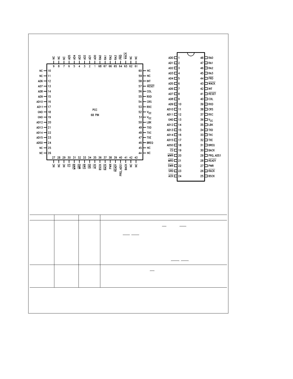
Connection Diagrams
Plastic Chip Carrier
TL/F/8582 – 5
Dual-In-Line Package
TL/F/8582 – 4
Order Number DP8390DN or DP8390DV
See NS Package Number N48A or V68A
5.0 Pin Descriptions
BUS INTERFACE PINS
Symbol
DIP Pin No
Function
Description
AD0 – AD15
1 – 12
I/O,Z
MULTIPLEXED ADDRESS/DATA BUS:
14 – 17
#
Register Access, with DMA inactive, CS low and ACK returned from NIC, pins
AD0 – AD7 are used to read/write register data. AD8 – AD15 float during I/O
transfers. SRD, SWR pins are used to select direction of transfer.
#
Bus Master with BACK input asserted.
During t1 of memory cycle AD0 – AD15 contain address.
During t2, t3, t4 AD0 – AD15 contain data (word transfer mode).
During t2, t3, t4 AD0 – AD7 contain data, AD8 – AD15 contain address
(byte transfer mode).
Direction of transfer is indicated by NIC on MWR, MRD lines.
ADS0
18
I/O,Z
ADDRESS STROBE 0
#
Input with DMA inactive and CS low, latches RA0–RA3 inputs on falling edge.
If high, data present on RA0–RA3 will flow through latch.
#
Output when Bus Master, latches address bits (A0–A15) to external memory
during DMA transfers.
4
5.0 Pin Descriptions
(Continued)
BUS INTERFACE PINS
(Continued)
Symbol
DIP Pin No
Function
Description
CS
19
I
CHIP SELECT:
Chip Select places controller in slave mode for mP access to
internal registers. Must be valid through data portion of bus cycle. RA0 – RA3 are
used to select the internal register. SWR and SRD select direction of data
transfer.
MWR
20
O,Z
MASTER WRITE STROBE:
Strobe for DMA transfers, active low during write
cycles (t2, t3, tw) to buffer memory. Rising edge coincides with the presence of
valid output data. TRI-STATE
É
until BACK asserted.
MRD
21
O,Z
MASTER READ STROBE:
Strobe for DMA transfers, active during read cycles
(t2, t3, tw) to buffer memory. Input data must be valid on rising edge of MRD.
TRI-STATE until BACK asserted.
SWR
22
I
SLAVE WRITE STROBE:
Strobe from CPU to write an internal register selected
by RA0 – RA3.
SRD
23
I
SLAVE READ STROBE:
Strobe from CPU to read an internal register selected
by RA0 – RA3.
ACK
24
O
ACKNOWLEDGE:
Active low when NIC grants access to CPU. Used to insert
WAIT states to CPU until NIC is synchronized for a register read or write
operation.
RA0 – RA3
45 – 48
I
REGISTER ADDRESS:
These four pins are used to select a register to be read
or written. The state of these inputs is ignored when the NIC is not in slave mode
(CS high).
PRD
44
O
PORT READ:
Enables data from external latch onto local bus during a memory
write cycle to local memory (remote write operation). This allows asynchronous
transfer of data from the system memory to local memory.
WACK
43
I
WRITE ACKNOWLEDGE:
Issued from system to NIC to indicate that data has
been written to the external latch. The NIC will begin a write cycle to place the
data in local memory.
INT
42
O
INTERRUPT:
Indicates that the NIC requires CPU attention after reception
transmission or completion of DMA transfers. The interrupt is cleared by writing
to the ISR. All interrupts are maskable.
RESET
41
I
RESET:
Reset is active low and places the NIC in a reset mode immediately, no
packets are transmitted or received by the NIC until STA bit is set. Affects
Command Register, Interrupt Mask Register, Data Configuration Register and
Transmit Configuration Register. The NIC will execute reset within 10 BUSK
cycles.
BREQ
31
O
BUS REQUEST:
Bus Request is an active high signal used to request the bus for
DMA transfers. This signal is automatically generated when the FIFO needs
servicing.
BACK
30
I
BUS ACKNOWLEDGE:
Bus Acknowledge is an active high signal indicating that
the CPU has granted the bus to the NIC. If immediate bus access is desired,
BREQ should be tied to BACK. Tying BACK to V
CC
will result in a deadlock.
PRQ, ADS1
29
O,Z
PORT REQUEST/ADDRESS STROBE 1
#
32-BIT MODE: If LAS is set in the Data Configuration Register, this line is
programmed as ADS1. It is used to strobe addresses A16 – A31 into external
latches. (A16 – A31 are the fixed addresses stored in RSAR0, RSAR1.) ADS1
will remain at TRI-STATE until BACK is received.
#
16-BIT MODE: If LAS is not set in the Data Configuration Register, this line is
programmed as PRQ and is used for Remote DMA Transfers. In this mode
PRQ will be a standard logic output.
NOTE: This line will power up as TRI-STATE until the Data Configuration
Register is programmed.
READY
28
I
READY:
This pin is set high to insert wait states during a DMA transfer. The NIC
will sample this signal at t3 during DMA transfers.
5
5.0 Pin Descriptions
(Continued)
BUS INTERFACE PINS
(Continued)
Symbol
DIP Pin No
Function
Description
PWR
27
O
PORT WRITE:
Strobe used to latch data from the NIC into external latch for
transfer to host memory during Remote Read transfers. The rising edge of PWR
coincides with the presence of valid data on the local bus.
RACK
26
I
READ ACKNOWLEDGE:
Indicates that the system DMA or host CPU has read
the data placed in the external latch by the NIC. The NIC will begin a read cycle
to update the latch.
BSCK
25
I
This clock is used to establish the period of the DMA memory cycle. Four clock
cycles (t1, t2, t3, t4) are used per DMA cycle. DMA transfers can be extended by
one BSCK increments using the READY input.
NETWORK INTERFACE PINS
COL
40
I
COLLISION DETECT:
This line becomes active when a collision has been
detected on the coaxial cable. During transmission this line is monitored after
preamble and synch have been transmitted. At the end of each transmission this
line is monitored for CD heartbeat.
RXD
39
I
RECEIVE DATA:
Serial NRZ data received from the ENDEC, clocked into the
NIC on the rising edge of RXC.
CRS
38
I
CARRIER SENSE:
This signal is provided by the ENDEC and indicates that
carrier is present. This signal is active high.
RXC
37
I
RECEIVE CLOCK:
Re-synchronized clock from the ENDEC used to clock data
from the ENDEC into the NIC.
LBK
35
O
LOOPBACK:
This output is set high when the NIC is programmed to perform a
loopback through the StarLAN ENDEC.
TXD
34
O
TRANSMIT DATA:
Serial NRZ Data output to the ENDEC. The data is valid on
the rising edge of TXC.
TXC
33
I
TRANSMIT CLOCK:
This clock is used to provide timing for internal operation
and to shift bits out of the transmit serializer. TXC is nominally a 1 MHz clock
provided by the ENDEC.
TXE
32
O
TRANSMIT ENABLE:
This output becomes active when the first bit of the
packet is valid on TXD and goes low after the last bit of the packet is clocked out
of TXD. This signal connects directly to the ENDEC. This signal is active high.
POWER
V
CC
36
a
5V DC is required. It is suggested that a decoupling capacitor be connected
between these pins. It is essential to provide a path to ground for the GND pin
GND
13
with the lowest possible impedance.
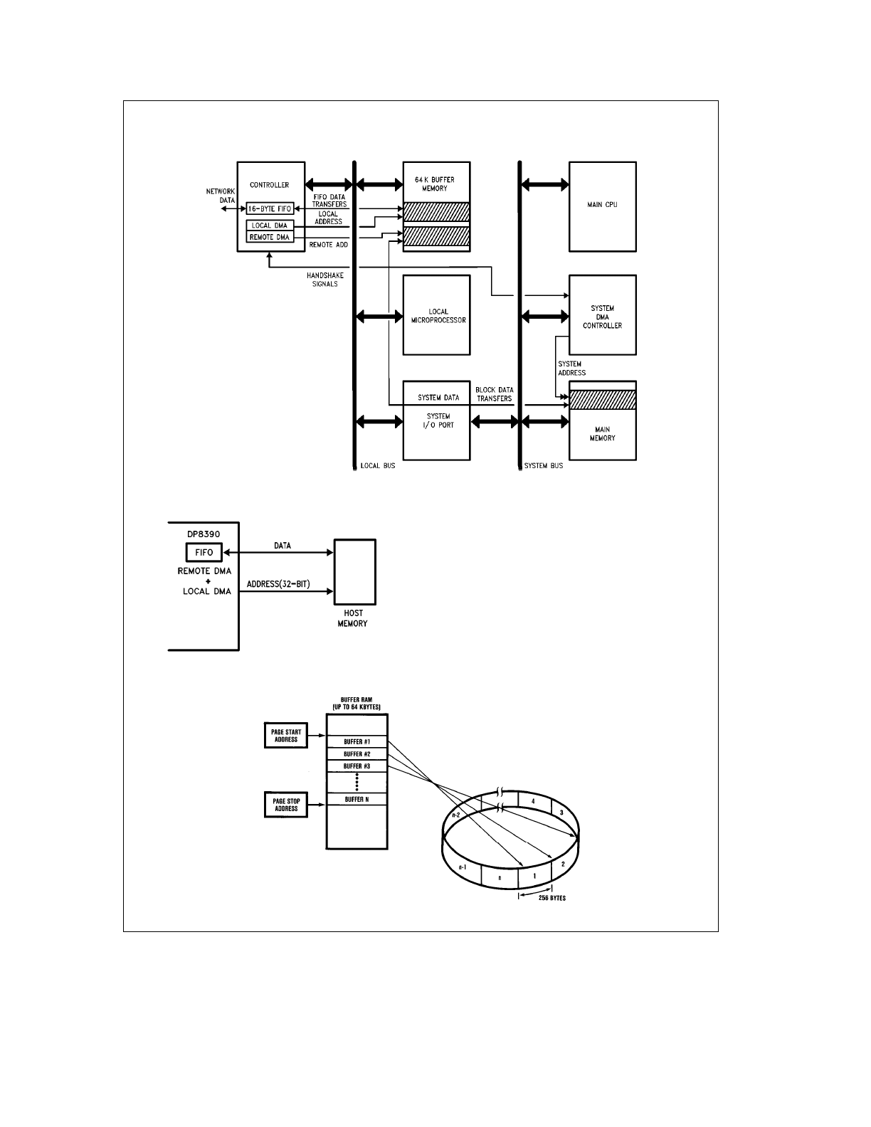
6.0 Direct Memory Access Control (DMA)
The DMA capabilities of the NIC greatly simplify use of the
DP8390D in typical configurations. The local DMA channel
transfers data between the FIFO and memory. On transmis-
sion, the packet is DMA’d from memory to the FIFO in
bursts. Should a collision occur (up to 15 times), the packet
is retransmitted with no processor intervention. On recep-
tion, packets are DMAed from the FIFO to the receive buffer
ring (as explained below).
A remote DMA channel is also provided on the NIC to ac-
complish transfers between a buffer memory and system
memory. The two DMA channels can alternatively be com-
bined to form a single 32-bit address with 8- or 16-bit data.
DUAL DMA CONFIGURATION
An example configuration using both the local and remote
DMA channels is shown below. Network activity is isolated
on a local bus, where the NIC’s local DMA channel per-
forms burst transfers between the buffer memory and the
NIC’s FIFO. The Remote DMA transfers data between the
buffer memory and the host memory via a bidirectional I/O
port. The Remote DMA provides local addressing capability
and is used as a slave DMA by the host. Host side address-
ing must be provided by a host DMA or the CPU. The NIC
allows Local and Remote DMA operations to be interleaved.
SINGLE CHANNEL DMA OPERATION
If desirable, the two DMA channels can be combined to
provide a 32-bit DMA address. The upper 16 bits of the 32-
bit address are static and are used to point to a 64k byte (or
32k word) page of memory where packets are to be re-
ceived and transmitted.
6
6.0 Direct Memory Access Control (DMA)
(Continued)
Dual Bus System
TL/F/8582 – 55
32-Bit DMA Operation
TL/F/8582 – 6
7.0 Packet Reception
The Local DMA receive channel uses a Buffer Ring Struc-
ture comprised of a series of contiguous fixed length 256
byte (128 word) buffers for storage of received packets. The
location of the Receive Buffer Ring is programmed in two
registers, a Page Start and a Page Stop Register. Ethernet
packets consist of a distribution of shorter link control pack-
ets and longer data packets, the 256 byte buffer length pro-
vides a good compromise between short packets and long-
er packets to most efficiently use memory. In addition these
buffers provide memory resources for storage of back-to-
back packets in loaded networks. The assignment of buffers
NIC Receive Buffer Ring
TL/F/8582 – 7
7
7.0 Packet Reception
(Continued)
for storing packets is controlled by Buffer Management Log-
ic in the NIC. The Buffer Management Logic provides three
basic functions: linking receive buffers for long packets, re-
covery of buffers when a packet is rejected, and recircula-
tion of buffer pages that have been read by the host.
At initialization, a portion of the 64k byte (or 32k word) ad-
dress space is reserved for the receive buffer ring. Two
eight bit registers, the Page Start Address Register
(PSTART) and the Page Stop Address Register (PSTOP)
define the physical boundaries of where the buffers reside.
The NIC treats the list of buffers as a logical ring; whenever
the DMA address reaches the Page Stop Address, the DMA
is reset to the Page Start Address.
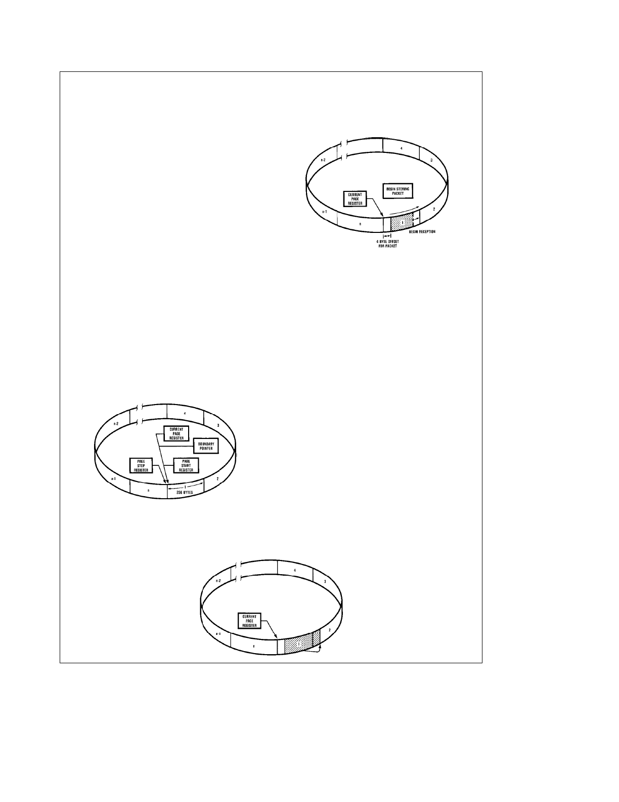
INITIALIZATION OF THE BUFFER RING
Two static registers and two working registers control the
operation of the Buffer Ring. These are the Page Start Reg-
ister, Page Stop Register (both described previously), the
Current Page Register and the Boundary Pointer Register.
The Current Page Register points to the first buffer used to
store a packet and is used to restore the DMA for writing
status to the Buffer Ring or for restoring the DMA address in
the event of a Runt packet, a CRC, or Frame Alignment
error. The Boundary Register points to the first packet in the
Ring not yet read by the host. If the local DMA address ever
reaches the Boundary, reception is aborted. The Boundary
Pointer is also used to initialize the Remote DMA for remov-
ing a packet and is advanced when a packet is removed. A
simple analogy to remember the function of these registers
is that the Current Page Register acts as a Write Pointer and
the Boundary Pointer acts as a Read Pointer.
Note 1:
At initialization, the Page Start Register value should be loaded into
both the Current Page Register and the Boundary Pointer Register.
Note 2:
The Page Start Register must not be initialized to 00H.
Receive Buffer Ring At Initialization
TL/F/8582 – 30
BEGINNING OF RECEPTION
When the first packet begins arriving the NIC begins storing
the packet at the location pointed to by the Current Page
Register. An offset of 4 bytes is saved in this first buffer to
allow room for storing receive status corresponding to this
packet.
Received Packet Enters Buffer Pages
TL/F/8582 – 31
LINKING RECEIVE BUFFER PAGES
If the length of the packet exhausts the first 256 byte buffer,
the DMA performs a forward link to the next buffer to store
the remainder of the packet. For a maximal length packet
the buffer logic will link six buffers to store the entire packet.
Buffers cannot be skipped when linking, a packet will always
be stored in contiguous buffers. Before the next buffer can
be linked, the Buffer Management Logic performs two com-
parisons. The first comparison tests for equality between
the DMA address of the next buffer and the contents of the
Page Stop Register. If the buffer address equals the Page
Stop Register, the buffer management logic will restore the
DMA to the first buffer in the Receive Buffer Ring value
programmed in the Page Start Address Register. The sec-
ond comparison tests for equality between the DMA ad-
dress of the next buffer address and the contents of the
Boundary Pointer Register. If the two values are equal the
reception is aborted. The Boundary Pointer Register can be
used to protect against overwriting any area in the receive
buffer ring that has not yet been read. When linking buffers,
buffer management will never cross this pointer, effectively
avoiding any overwrites. If the buffer address does not
match either the Boundary Pointer or Page Stop Address,
the link to the next buffer is performed.
Linking Buffers
Before the DMA can enter the next contiguous 256 byte
buffer, the address is checked for equality to PSTOP and to
the Boundary Pointer. If neither are reached, the DMA is
allowed to use the next buffer.
Linking Receive Buffer Pages
1) Check for e to PSTOP
2) Check for e to Boundary
TL/F/8582 – 32
8
7.0 Packet Reception
(Continued)
Received Packet Aborted if It Hits Boundary Pointer
TL/F/8582 – 8
Buffer Ring Overflow
If the Buffer Ring has been filled and the DMA reaches the
Boundary Pointer Address, reception of the incoming pack-
et will be aborted by the NIC. Thus, the packets previously
received and still contained in the Ring will not be de-
stroyed.
In a heavily loaded network environment the local DMA may
be disabled, preventing the NIC from buffering packets from
the network. To guarantee this will not happen, a software
reset must be issued during all Receive Buffer Ring over-
flows (indicated by the OVW bit in the Interrupt Status Reg-
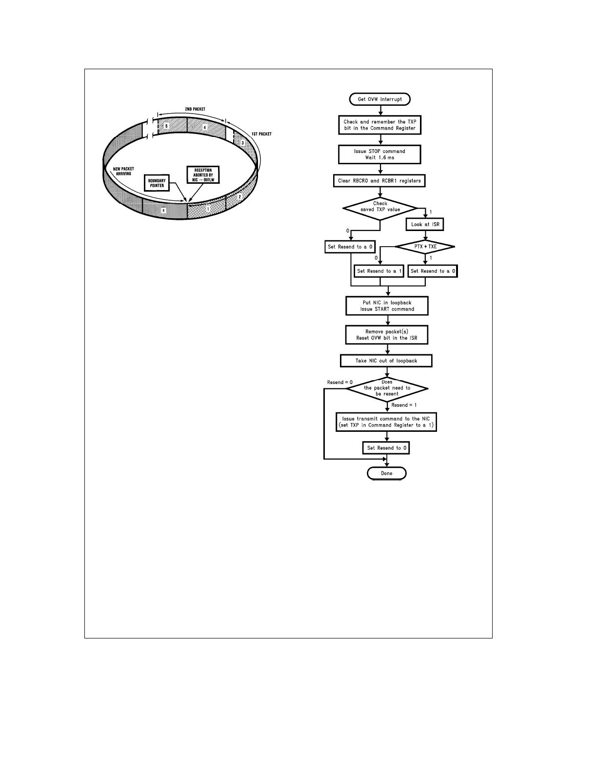
ister). The following procedure is required to recover
from a Receiver Buffer Ring Overflow.
If this routine is not adhered to, the NIC may act in an unpre-
dictable manner. It should also be noted that it is not per-
missible to service an overflow interrupt by continuing to
empty packets from the receive buffer without implementing
the prescribed overflow routine. A flow chart of the NIC’s
overflow routine can be found at the right.
Note:
It is necessary to define a variable in the driver, which will be called
‘‘Resend’’.
1. Read and store the value of the TXP bit in the NIC’s
Command Register.
2. Issue the STOP command to the NIC. This is accom-
plished be setting the STP bit in the NIC’s Command
Register. Writing 21H to the Command Register will stop
the NIC.
Note:
If the STP is set when a transmission is in progress, the RST bit may
not be set. In this case, the NIC is guaranteed to be reset after the
longest packet time (1500 bytes e 1.2 ms). For the DP8390D (but not
for the DP8390B), the NIC will be reset within 2 microseconds after
the STP bit is set and Loopback mode 1 is programmed.
3. Wait for at least 1.6 ms. Since the NIC will complete any
transmission or reception that is in progress, it is neces-
sary to time out for the maximum possible duration of an
Ethernet transmission or reception. By waiting 1.6 ms this
is achieved with some guard band added. Previously, it
was recommended that the RST bit of the Interrupt
Status Register be polled to insure that the pending
transmission or reception is completed. This bit is not a
reliable indicator and subsequently should be ignored.
4. Clear the NIC’s Remote Byte Count registers (RBCR0
and RBCR1).
TL/F/8582 – 95
Overflow Routine Flow Chart
5. Read the stored value of the TXP bit from step 1, above.
If this value is a 0, set the ‘‘Resend’’ variable to a 0 and
jump to step 6.
If this value is a 1, read the NIC’s Interrupt Status Regis-
ter. If either the Packet Transmitted bit (PTX) or Trans-
mit Error bit (TXE) is set to a 1, set the ‘‘Resend’’ vari-
able to a 0 and jump to step 6. If neither of these bits is
set, place a 1 in the ‘‘Resend’’ variable and jump to step
6.
This step determines if there was a transmission in prog-
ress when the stop command was issued in step 2. If
there was a transmission in progress, the NIC’s ISR is
read to determine whether or not the packet was recog-
nized by the NIC. If neither the PTX nor TXE bit was set,
9
7.0 Packet Reception
(Continued)
then the packet will essentially be lost and re-transmit-
ted only after a time-out takes place in the upper level
software. By determining that the packet was lost at the
driver level, a transmit command can be reissued to the
NIC once the overflow routine is completed (as in step
11). Also, it is possible for the NIC to defer indefinitely,
when it is stopped on a busy network. Step 5 also allevi-
ates this problem. Step 5 is essential and should not be
omitted from the overflow routine, in order for the NIC to
operate correctly.
6. Place the NIC in either mode 1 or mode 2 loopback. This
can be accomplished by setting bits D2 and D1, of the
Transmit Configuration Register, to ‘‘0,1’’ or ‘‘1,0’’, re-
spectively.
7. Issue the START command to the NIC. This can be ac-
complished by writing 22H to the Command Register.
This is necessary to activate the NIC’s Remote DMA
channel.
8. Remove one or more packets from the receive buffer
ring.
9. Reset the overwrite warning (OVW, overflow) bit in the
Interrupt Status Register.
10. Take the NIC out of loopback. This is done by writing the
Transmit Configuration Register with the value it con-
tains during normal operation. (Bits D2 and D1 should
both be programmed to 0.)
11. If the ‘‘Resend’’ variable is set to a 1, reset the ‘‘Re-
send’’ variable and reissue the transmit command. This
is done by writing a value of 26H to the Command Reg-
ister. If the ‘‘Resend’’ variable is 0, nothing needs to be
done.
Note:
If Remote DMA is not being used, the NIC does not need to be started
before packets can be removed from the receive buffer ring. Hence,
step 8 could be done before step 7.
END OF PACKET OPERATIONS
At the end of the packet the NIC determines whether the
received packet is to be accepted or rejected. It either
branches to a routine to store the Buffer Header or to anoth-
er routine that recovers the buffers used to store the packet.
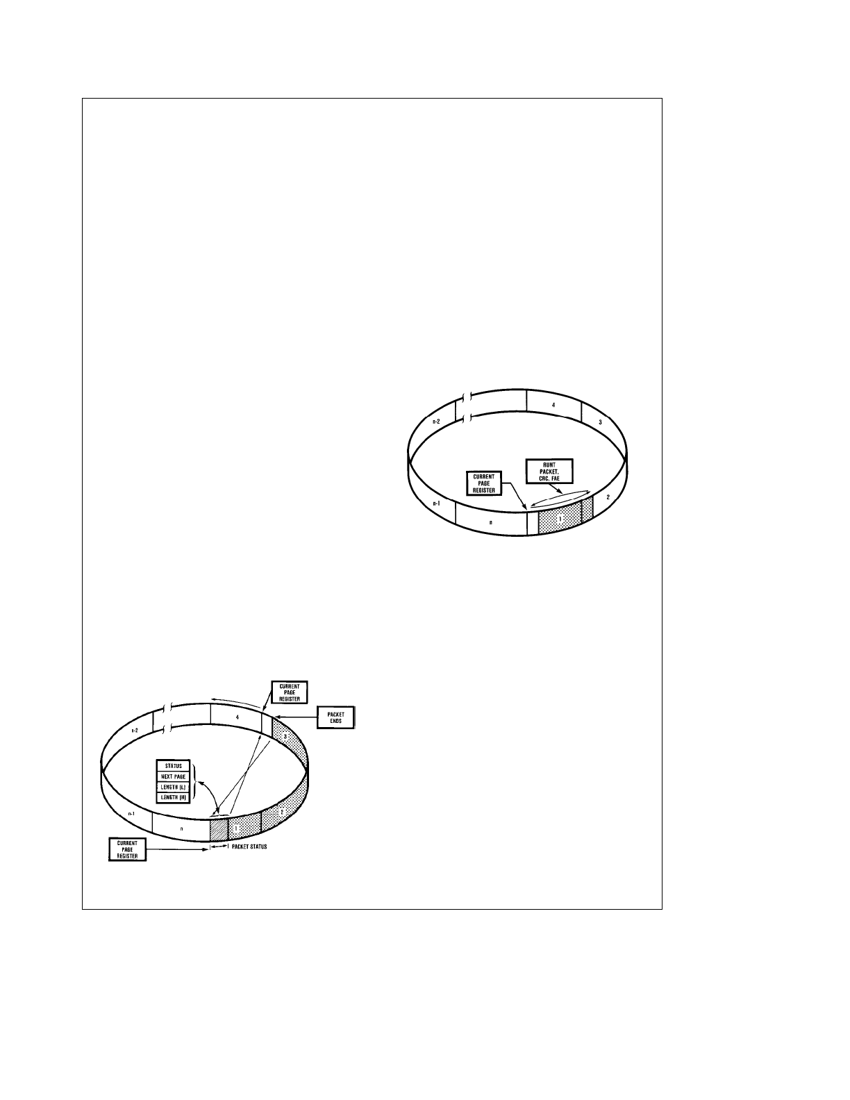
SUCCESSFUL RECEPTION
If the packet is successfully received as shown, the DMA is
restored to the first buffer used to store the packet (pointed
Termination of Received PacketÐPacket Accepted
TL/F/8582 – 10
to by the Current Page Register). The DMA then stores the
Receive Status, a Pointer to where the next packet will be
stored (Buffer 4) and the number of received bytes. Note
that the remaining bytes in the last buffer are discarded and
reception of the next packet begins on the next empty 256-
byte buffer boundary. The Current Page Register is then
initialized to the next available buffer in the Buffer Ring. (The
location of the next buffer had been previously calculated
and temporarily stored in an internal scratchpad register.)
BUFFER RECOVERY FOR REJECTED PACKETS
If the packet is a runt packet or contains CRC or Frame
Alignment errors, it is rejected. The buffer management log-
ic resets the DMA back to the first buffer page used to store
the packet (pointed to by CURR), recovering all buffers that
had been used to store the rejected packet. This operation
will not be performed if the NIC is programmed to accept
either runt packets or packets with CRC or Frame Alignment
errors. The received CRC is always stored in buffer memory
after the last byte of received data for the packet.
Termination of Received PacketÐPacket Rejected
TL/F/8582 – 13
Error Recovery
If the packet is rejected as shown, the DMA is restored by
the NIC by reprogramming the DMA starting address point-
ed to by the Current Page Register.
REMOVING PACKETS FROM THE RING
Packets are removed from the ring using the Remote DMA
or an external device. When using the Remote DMA the
Send Packet command can be used. This programs the Re-
mote DMA to automatically remove the received packet
pointed to by the Boundary Pointer. At the end of the trans-
fer, the NIC moves the Boundary Pointer, freeing additional
buffers for reception. The Boundary Pointer can also be
moved manually by programming the Boundary Register.
Care should be taken to keep the Boundary Pointer at least
one buffer behind the Current Page Pointer.
The following is a suggested method for maintaining the
Receive Buffer Ring pointers.
1. At initialization, set up a software variable (nextÐpkt) to
indicate where the next packet will be read. At the begin-
ning of each Remote Read DMA operation, the value of
nextÐpkt will be loaded into RSAR0 and RSAR1.
2. When initializing the NIC set:
BNDRY
e
PSTART
CURR
e
PSTART
a
1
nextÐpkt
e
PSTART
a
1
10
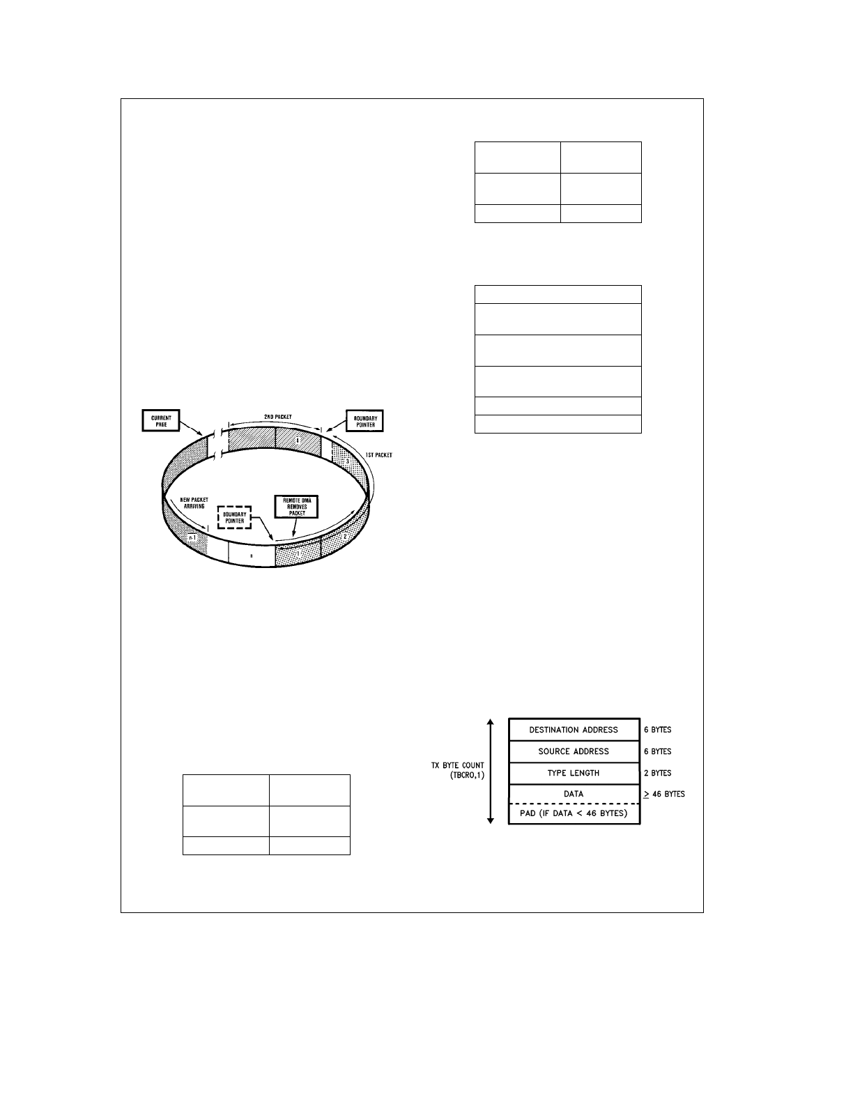
7.0 Packet Reception
(Continued)
3. After a packet is DMAed from the Receive Buffer Ring,
the Next Page Pointer (second byte in NIC buffer header)
is used to update BNDRY and nextÐpkt.
nextÐpkt
e
Next Page Pointer
BNDRY
e
Next Page Pointer
b
1
If BNDRY
k
PSTART then BNDRY
e
PSTOP
b
1
Note the size of the Receive Buffer Ring is reduced by one
256-byte buffer; this will not, however, impede the operation
of the NIC.
In StarLAN applications using bus clock frequencies greater
than 4 MHz, the NIC does not update the buffer header
information properly because of the disparity between the
network and bus clock speeds. The lower byte count is cop-
ied twice into the third and fourth locations of the buffer
header and the upper byte count is not written. The upper
byte count, however, can be calculated from the current
next page pointer (second byte in the buffer header) and the
previous next page pointer (stored in memory by the CPU).
The following routine calculates the upper byte count and
allows StarLAN applications to be insensitive to bus clock
speeds. NextÐpkt is defined similarly as above.
1st Received Packet Removed By Remote DMA
TL/F/8582 – 57
upper byte count
e
next page pointer
b
nextÐpkt
b
1
if (upper byte count)
k
0 then
upper byte count
e
(PSTOP
b
nextÐpkt)
a
(next page pointer
b
PSTART)
b
1
if (lower byte count)
l
0 fch then
upper byte count
e
upper byte count
a
1
STORAGE FORMAT FOR RECEIVED PACKETS
The following diagrams describe the format for how re-
ceived packets are placed into memory by the local DMA
channel. These modes are selected in the Data Configura-
tion Register.
Storage Format
AD15
AD8
AD7
AD0
Next Packet
Receive
Pointer
Status
Receive
Receive
Byte Count 1
Byte Count 0
Byte 2
Byte 1
BOS e 0, WTS e 1 in Data Configuration Register.
This format used with Series 32000 808X type processors.
AD15
AD8
AD7
AD0
Next Packet
Receive
Pointer
Status
Receive
Receive
Byte Count 0
Byte Count 1
Byte 1
Byte 2
BOS e 1, WTS e 1 in Data Configuration Register.
This format used with 68000 type processors.
Note:
The Receive Byte Count ordering remains the same for BOSe0 or 1.
AD7
AD0
Receive Status
Next Packet
Pointer
Receive Byte
Count 0
Receive Byte
Count 1
Byte 0
Byte 1
BOS e 0, WTS e 0 in Data Configuration Register.
This format used with general 8-bit CPUs.
8.0 Packet Transmission
The Local DMA is also used during transmission of a pack-
et. Three registers control the DMA transfer during trans-
mission, a Transmit Page Start Address Register (TPSR)
and the Transmit Byte Count Registers (TBCR0,1). When
the NIC receives a command to transmit the packet pointed
to by these registers, buffer memory data will be moved into
the FIFO as required during transmission. The NIC will gen-
erate and append the preamble, synch and CRC fields.
TRANSMIT PACKET ASSEMBLY
The NIC requires a contiguous assembled packet with the
format shown. The transmit byte count includes the Destina-
tion Address, Source Address, Length Field and Data. It
does not include preamble and CRC. When transmitting
data smaller than 46 bytes, the packet must be padded to a
minimum size of 64 bytes. The programmer is responsible
for adding and stripping pad bytes.
General Transmit Packet Format
TL/F/8582 – 58
11
8.0 Packet Transmission
(Continued)
TRANSMISSION
Prior to transmission, the TPSR (Transmit Page Start Regis-
ter) and TBCR0, TBCR1 (Transmit Byte Count Registers)
must be initialized. To initiate transmission of the packet the
TXP bit in the Command Register is set. The Transmit
Status Register (TSR) is cleared and the NIC begins to pre-
fetch transmit data from memory (unless the NIC is currently
receiving). If the interframe gap has timed out the NIC will
begin transmission.
CONDITIONS REQUIRED TO BEGIN TRANSMISSION
In order to transmit a packet, the following three conditions
must be met:
1. The Interframe Gap Timer has timed out the first 6.4 ms
of the Interframe Gap (See appendix for Interframe Gap
Flowchart)
2. At least one byte has entered the FIFO. (This indicates
that the burst transfer has been started)
3. If the NIC had collided, the backoff timer has expired.
In typical systems the NIC has already prefetched the first
burst of bytes before the 6.4 ms timer expires. The time
during which NIC transmits preamble can also be used to
load the FIFO.
Note:
If carrier sense is asserted before a byte has been loaded into the
FIFO, the NIC will become a receiver.
COLLISION RECOVERY
During transmission, the Buffer Management logic monitors
the transmit circuitry to determine if a collision has occurred.
If a collision is detected, the Buffer Management logic will
reset the FIFO and restore the Transmit DMA pointers for
retransmission of the packet. The COL bit will be set in the
TSR and the NCR (Number of Collisions Register) will be
incremented. If 15 retransmissions each result in a collision
the transmission will be aborted and the ABT bit in the TSR
will be set.
Note:
NCR reads as zeroes if excessive collisions are encountered.
TRANSMIT PACKET ASSEMBLY FORMAT
The following diagrams describe the format for how packets
must be assembled prior to transmission for different byte
ordering schemes. The various formats are selected in the
Data Configuration Register.
D15
D8 D7
D0
DA1
DA0
DA3
DA2
DA5
DA4
SA1
DA0
SA3
DA2
SA5
DA4
T/L1
T/L0
DATA 1
DATA 0
BOS e 0, WTS e 1 in Data Configuration Register.
This format is used with Series 32000, 808X type proces-
sors.
D15
D8 D7
D0
DA0
DA1
DA2
DA3
DA4
DA5
SA0
SA1
SA2
SA3
SA4
SA5
T/L0
T/L1
DATA 0
DATA 1
BOS e 1, WTS e 1 in Data Configuration Register.
This format is used with 68000 type processors.
D7
D0
DA0
DA1
DA2
DA3
DA4
DA5
SA0
SA1
SA2
SA3
BOS e 0, WTS e 0 in Data Configuration Register.
This format is used with general 8-bit CPUs.
Note:
All examples above will result in a transmission of a packet in order of
DA0, DA1, DA2, DA3 . . . bits within each byte will be transmitted least
significant bit first.
DA e Destination Address
SA e Source Address
T/L e Type/Length Field
9.0 Remote DMA
The Remote DMA channel is used to both assemble pack-
ets for transmission, and to remove received packets from
the Receive Buffer Ring. It may also be used as a general
purpose slave DMA channel for moving blocks of data or
commands between host memory and local buffer memory.
There are three modes of operation, Remote Write, Remote
Read, or Send Packet.
Two register pairs are used to control the Remote DMA, a
Remote Start Address (RSAR0, RSAR1) and a Remote
Byte Count (RBCR0, RBCR1) register pair. The Start Ad-
dress Register pair points to the beginning of the block to be
moved while the Byte Count Register pair is used to indicate
the number of bytes to be transferred. Full handshake logic
is provided to move data between local buffer memory and
a bidirectional I/O port.
12
9.0 Remote DMA
(Continued)
REMOTE WRITE
A Remote Write transfer is used to move a block of data
from the host into local buffer memory. The Remote DMA
will read data from the I/O port and sequentially write it to
local buffer memory beginning at the Remote Start Address.
The DMA Address will be incremented and the Byte Coun-
ter will be decremented after each transfer. The DMA is
terminated when the Remote Byte Count Register reaches
a count of zero.
REMOTE READ
A Remote Read transfer is used to move a block of data
from local buffer memory to the host. The Remote DMA will
sequentially read data from the local buffer memory, begin-
ning at the Remote Start Address, and write data to the I/O
port. The DMA Address will be incremented and the Byte
Counter will be decremented after each transfer. The DMA
is terminated when the Remote Byte Count Register reach-
es zero.
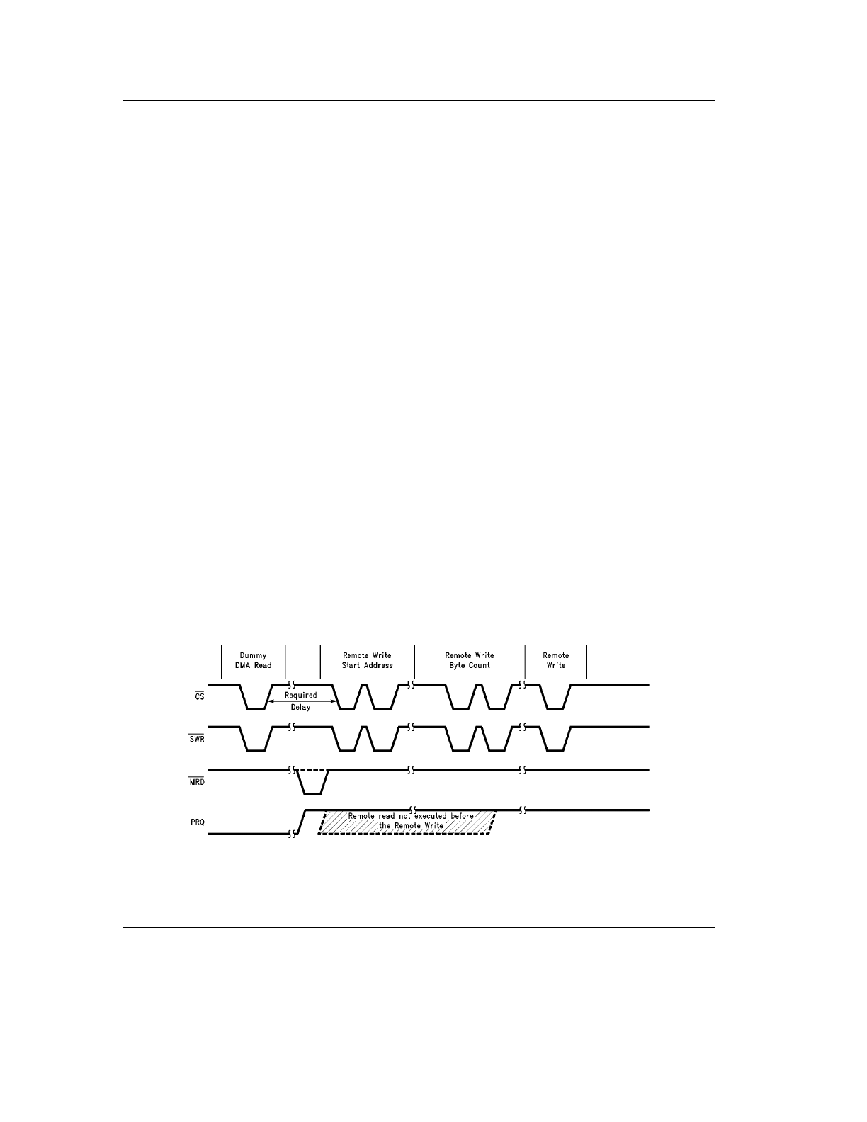
REMOTE DMA WRITE
Setting PRQ Using the Remote Read
Under certain conditions the NIC’s bus state machine may
issue /MWR and /PRD before PRQ for the first DMA trans-
fer of a Remote Write Command. If this occurs this could
cause data corruption, or cause the remote DMA count to
be different from the main CPU count causing the system to
‘‘lock up’’.
To prevent this condition when implementing a Remote
DMA Write, the Remote DMA Write command should first
be preceded by a Remote DMA Read command to insure
that the PRQ signal is asserted before the NIC starts its port
read cycle. The reason for this is that the state machine that
asserts PRQ runs independently of the state machine that
controls the DMA signals. The DMA machine assumes that
PRQ is asserted, but actually may not be. To remedy this
situation, a single Remote Read cycle should be inserted
before the actual DMA Write Command is given. This will
ensure that PRQ is asserted when the Remote DMA Write is
subsequently executed. This single Remote Read cycle is
called a ‘‘dummy Remote Read.’’ In order for the dummy
Remote Read cycle to operate correctly, the Start Address
should be programmed to a known, safe location in the buff-
er memory space, and the Remote Byte Count should be
progammed to a value greater than 1. This will ensure that
the master read cycle is performed safely, eliminating the
possiblity of data corruption.
Remote Write with High Speed Buses
When implementing the Remote DMA Write solution in pre-
vious section with high speed buses and CPU’s, timing
problems may cause the system to hang. Therefore addi-
tional considerations are required.
The problem occurs when the system can execute the dum-
my Remote Read and then start the Remote Write before
the NIC has had a chance to execute the Remote Read. If
this happens the PRQ signal will not get set, and the Re-
mote Byte Count and Remote Start Address for the Remote
Write operation could be corrupted. This is shown by the
hatched waveforms in the timing diagram below. The execu-
tion of the Remote Read can be delayed by the local DMA
operations (particularly during end-of-packet processing).
To ensure the dummy Remote Read does execute, a delay
must be inserted between writing the Remote Read Com-
mand, and starting to write the Remote Write Start Address.
(This time is designated in figure below by the delay arrows.)
The recommended method to avoid this problem is, after
the Remote Read command is given, to poll both bytes of
the Current Remote DMA Address Registers. When the ad-
dress has incremented, PRQ has been set. Software should
recognize this and then start the Remote Write.
An additional caution for high speed systems is that the
polling must follow guidelines specified at the end of Sec-
tion 13. That is, there must be at least 4 bus clocks between
chip selects. (For example, when BSCK
e
20 MHz, then
this time should be 200 ns.)
The general flow for executing a Remote Write is:
1. Set Remote Byte Count to a value
l
1 and Remote Start
Address to unused RAM (one location before the transmit
start address is usually a safe location).
TL/F/8582 – 96
Timing Diagram for Dummy Remote Read
Note:
The dashed lines indicate incorrect timing.
13
9.0 Remote DMA
(Continued)
2. Issue the ‘‘dummy’’ Remote Read command.
3. Read the Current Remote DMA Address (CRDA) (both
bytes).
4. Compare to previous CRDA value if different go to 6.
5. Delay and jump to 3.
6. Set up for the Remote Write command, by setting the
Remote Byte Count and the Remote Start Address (note
that if the Remote Byte count in step 1 can be set to the
tramsmit byte count plus one, and the Remote Start Ad-
dress to one less, these will now be incremented to the
correct values.)
7. Issue the Remote Write command.
FIFO AND BUS OPERATIONS
Overview
To accommodate the different rates at which data comes
from (or goes to) the network and goes to (or comes from)
the system memory, the NIC contains a 16-byte FIFO for
buffering data between the bus and the media. The FIFO
threshold is programmable, allowing filling (or emptying) the
FIFO at different rates. When the FIFO has filled to its pro-
grammed threshold, the local DMA channel transfers these
bytes (or words) into local memory. It is crucial that the local
DMA is given access to the bus within a minimum bus laten-
cy time; otherwise a FIFO underrun (or overrun) occurs.
To understand FIFO underruns or overruns, there are two
causes which produce this conditionÐ
1) the bus latency is so long that the FIFO has filled (or
emptied) from the network before the local DMA has
serviced the FIFO.
2) the bus latency or bus data rate has slowed the through-
put of the local DMA to point where it is slower than the
network data rate (10 Mb/s). This second condition is
also dependent upon DMA clock and word width (byte
wide or word wide).
The worst case condition ultimately limits the overall bus
latency which the NIC can tolerate.
FIFO Underrun and Transmit Enable
During transmission, if a FIFO underrun occurs, the Trans-
mit enable (TXE) output may remain high (active). Generally,
this will cause a very large packet to be transmitted onto the
network. The jabber feature of the transceiver will terminate
the transmission, and reset TXE.
To prevent this problem, a properly designed system will not
allow FIFO underruns by giving the NIC a bus acknowledge
within time shown in the maximum bus latency curves
shown and described later.
FIFO at the Beginning of Receive
At the beginning of reception, the NIC stores entire Address
field of each incoming packet in the FIFO to determine
whether the packet matches its Physical Address Registers
or maps to one of its Multicast Registers. This causes the
FIFO to accumulate 8 bytes. Furthermore, there are some
synchronization delays in the DMA PLA. Thus, the actual
time that BREQ is asserted from the time the Start of Frame
Delimiter (SFD) is detected is 7.8 ms. This operation affects
the bus latencies at 2 and 4 byte thresholds during the first
receive BREQ since the FIFO must be filled to 8 bytes (4
words) before issuing a BREQ.
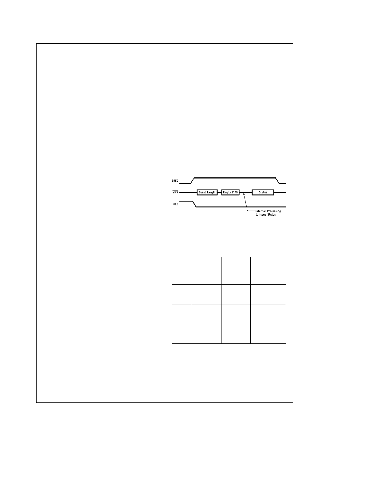
FIFO Operation at the End of Receive
When Carrier Sense goes low, the NIC enters its end of
packet processing sequence, emptying its FIFO and writing
the status information at the beginning of the packet, figure
below. This NIC holds onto the bus for the entire sequence.
The longest time BREQ may be extended occurs when a
packet ends just as the NIC performs its last FIFO burst.
The NIC, in this case, performs a programmed burst transfer
followed by flushing the remaining bytes in the FIFO, and
completes by writing the header information to memory. The
following steps occur during this sequence.
1) NIC issues BREQ because the FIFO threshold has been
reached.
2) During the burst, packet ends, resulting in BREQ extend-
ed.
3) NIC flushes remaining bytes from FIFO.
4) NIC performs internal processing to prepare for writing
the header.
5) NIC writes 4-byte (2-word) header.
6) NIC deasserts BREQ.
TL/F/8582 – 97
End of Packet Processing
End of Packet Processing (EOPP) times for 10 MHz and
20 MHz have been tabulated in the table below.
End of Packet Processing Times for Various FIFO
Thresholds, Bus Clocks and Transfer Modes
Mode
Threshold
Bus Clock
EOPP
Byte
2 bytes
7.0 ms
4 bytes
10 MHz
8.6 ms
8 bytes
11.0 ms
Byte
2 bytes
3.6 ms
4 bytes
20 MHz
4.2 ms
8 bytes
5.0 ms
Word
2 bytes
5.4 ms
4 bytes
10 MHz
6.2 ms
8 bytes
7.4 ms
Word
2 bytes
3.0 ms
4 bytes
20 MHz
3.2 ms
8 bytes
3.6 ms
Threshold Detection (Bus Latency)
To assure that no overwriting of data in the FIFO, the FIFO
logic flags a FIFO overrun as the 13th byte is written into the
FIFO, effectively shortening the FIFO to 13 bytes. The FIFO
logic also operates differently in Byte Mode and in Word
Mode. In Byte Mode, a threshold is indicated when the n
a
1
14
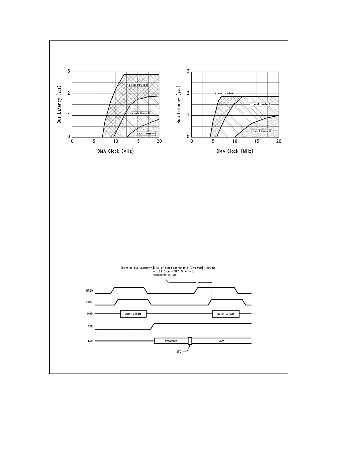
9.0 Remote DMA
(Continued)
Maximum Bus Latency for Byte Mode
TL/F/8582 – 98
Maximum Bus Latency for Word Mode
TL/F/8582 – 99
byte has entered the FIFO; thus, with an 8 byte threshold,
the NIC issues Bus Request (BREQ) when the 9th byte has
entered the FIFO. For Word Mode, BREQ is not generated
until the n
a
2 bytes have entered the FIFO. Thus, with a 4
word threshold (equivalent to 8 byte threshold), BREQ is
issued when the 10th byte has entered the FIFO. The two
graphs, the figures above, indicate the maximum allowable
bus latency for Word and Byte transfer modes.
The FIFO at the Beginning of Transmit
Before transmitting, the NIC performs a prefetch from mem-
ory to load the FIFO. The number of bytes prefetched is the
programmed FIFO threshold. The next BREQ is not issued
until after the NIC actually begins trasmitting data, i.e., after
SFD. The Transmit Prefetch diagram illustrates this process.
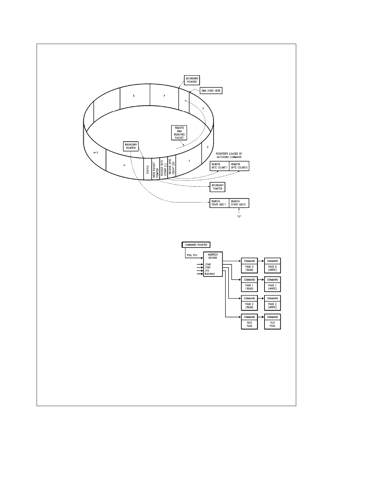
SEND PACKET COMMAND
The Remote DMA channel can be automatically initialized
to transfer a single packet from the Receive Buffer Ring.
The CPU begins this transfer by issuing a ‘‘Send Packet’’
Command. The DMA will be initialized to the value of the
Boundary Pointer Register and the Remote Byte Count
Register pair (RBCR0, RBCR1) will be initialized to the value
of the Receive Byte Count fields found in the Buffer Header
of each packet. After the data is transferred, the Boundary
Pointer is advanced to allow the buffers to be used for new
receive packets. The Remote Read will terminate when the
Byte Count equals zero. The Remote DMA is then prepared
to read the next packet from the Receive Buffer Ring. If the
DMA pointer crosses the Page Stop Register, it is reset to
the Page Start Address. This allows the Remote DMA to
remove packets that have wrapped around to the top of the
Receive Buffer Ring.
Note 1:
In order for the NIC to correctly execute the Send Packet Com-
mand, the upper Remote Byte Count Register (RBCR1) must first
be loaded with 0FH.
Note 2:
The Send Packet command cannot be used with 68000 type proc-
essors.
Transmit Prefetch Timing
TL/F/8582 – A0
15
9.0 Remote DMA
(Continued)
Remote DMA Autoinitialization from Buffer Ring
TL/F/8582 – 59
10.0 Internal Registers
All registers are 8-bit wide and mapped into two pages
which are selected in the Command Register (PS0, PS1).
Pins RA0 – RA3 are used to address registers within each
page. Page 0 registers are those registers which are com-
monly accessed during NIC operation while page 1 registers
are used primarily for initialization. The registers are parti-
tioned to avoid having to perform two write/read cycles to
access commonly used registers.
10.1 REGISTER ADDRESS MAPPING
TL/F/8582 – 60
16

10.0 Internal Registers
(Continued)
10.2 REGISTER ADDRESS ASSIGNMENTS
Page 0 Address Assignments (PS1
e
0, PS0
e
0)
RA0 – RA3
RD
WR
00H
Command (CR)
Command (CR)
01H
Current Local DMA
Page Start Register
Address 0 (CLDA0)
(PSTART)
02H
Current Local DMA
Page Stop Register
Address 1 (CLDA1)
(PSTOP)
03H
Boundary Pointer
Boundary Pointer
(BNRY)
(BNRY)
04H
Transmit Status
Transmit Page Start
Register (TSR)
Address (TPSR)
05H
Number of Collisions
Transmit Byte Count
Register (NCR)
Register 0 (TBCR0)
06H
FIFO (FIFO)
Transmit Byte Count
Register 1 (TBCR1)
07H
Interrupt Status
Interrupt Status
Register (ISR)
Register (ISR)
08H
Current Remote DMA Remote Start Address
Address 0 (CRDA0)
Register 0 (RSAR0)
09H
Current Remote DMA Remote Start Address
Address 1 (CRDA1)
Register 1 (RSAR1)
0AH
Reserved
Remote Byte Count
Register 0 (RBCR0)
0BH
Reserved
Remote Byte Count
Register 1 (RBCR1)
0CH
Receive Status
Receive Configuration
Register (RSR)
Register (RCR)
0DH
Tally Counter 0
Transmit Configuration
(Frame Alignment
Register (TCR)
Errors) (CNTR0)
0EH
Tally Counter 1
Data Configuration
(CRC Errors)
Register (DCR)
(CNTR1)
0FH
Tally Counter 2
Interrupt Mask
(Missed Packet
Register (IMR)
Errors) (CNTR2)
Page 1 Address Assignments (PS1
e
0, PS0
e
1)
RA0 – RA3
RD
WR
00H
Command (CR)
Command (CR)
01H
Physical Address
Physical Address
Register 0 (PAR0)
Register 0 (PAR0)
02H
Physical Address
Physical Address
Register 1 (PAR1)
Register 1 (PAR1)
03H
Physical Address
Physical Address
Register 2 (PAR2)
Register 2 (PAR2)
04H
Physical Address
Physical Address
Register 3 (PAR3)
Register 3 (PAR3)
05H
Physical Address
Physical Address
Register 4 (PAR4)
Register 4 (PAR4)
06H
Physical Address
Physical Address
Register 5 (PAR5)
Register 5 (PAR5)
07H
Current Page
Current Page
Register (CURR)
Register (CURR)
08H
Multicast Address
Multicast Address
Register 0 (MAR0)
Register 0 (MAR0)
09H
Multicast Address
Multicast Address
Register 1 (MAR1)
Register 1 (MAR1)
0AH
Multicast Address
Multicast Address
Register 2 (MAR2)
Register 2 (MAR2)
0BH
Multicast Address
Multicast Address
Register 3 (MAR3)
Register 3 (MAR3)
0CH
Multicast Address
Multicast Address
Register 4 (MAR4)
Register 4 (MAR4)
0DH
Multicast Address
Multicast Address
Register 5 (MAR5)
Register 5 (MAR5)
0EH
Multicast Address
Multicast Address
Register 6 (MAR6)
Register 6 (MAR6)
0FH
Multicast Address
Multicast Address
Register 7 (MAR7)
Register 7 (MAR7)
17
10.0 Internal Registers
(Continued)
Page 2 Address Assignments (PS1
e
1, PS0
e
0)
RA0 – RA3
RD
WR
00H
Command (CR)
Command (CR)
01H
Page Start Register
Current Local DMA
(PSTART)
Address 0 (CLDA0)
02H
Page Stop Register
Current Local DMA
(PSTOP)
Address 1 (CLDA1)
03H
Remote Next Packet
Remote Next Packet
Pointer
Pointer
04H
Transmit Page Start
Reserved
Address (TPSR)
05H
Local Next Packet
Local Next Packet
Pointer
Pointer
06H
Address Counter
Address Counter
(Upper)
(Upper)
07H
Address Counter
Address Counter
(Lower)
(Lower)
RA0 – RA3
RD
WR
08H
Reserved
Reserved
09H
Reserved
Reserved
0AH
Reserved
Reserved
0BH
Reserved
Reserved
0CH
Receive Configuration
Reserved
Register (RCR)
0DH
Transmit Configuration
Reserved
Register (TCR)
0EH
Data Configuration
Reserved
Register (DCR)
0FH
Interrupt Mask Register
Reserved
(IMR)
Note:
Page 2 registers should only be accessed for diagnostic purposes.
They should not be modified during normal operation.
Page 3 should never be modified.
18
10.0 Internal Registers
(Continued)
10.3 Register Descriptions
COMMAND REGISTER (CR)
00H (READ/WRITE)
The Command Register is used to initiate transmissions, enable or disable Remote DMA operations and to select register
pages. To issue a command the microprocessor sets the corresponding bit(s) (RD2, RD1, RD0, TXP). Further commands may
be overlapped, but with the following rules: (1) If a transmit command overlaps with a remote DMA operation, bits RD0, RD1,
and RD2 must be maintained for the remote DMA command when setting the TXP bit. Note, if a remote DMA command is re-is-
sued when giving the transmit command, the DMA will complete immediately if the remote byte count register have not been re-
initialized. (2) If a remote DMA operation overlaps a transmission, RD0, RD1, and RD2 may be written with the desired values
and a ‘‘0’’ written to the TXP bit. Writing a ‘‘0’’ to this bit has no effect. (3) A remote write DMA may not overlap remote read
operation or visa versa. Either of these operations must either complete or be aborted before the other operation may start.
Bits PS1, PS0, RD2, and STP may be set any time.
7
6
5
4
3
2
1
0
PS1
PS0
RD2
RD1
RD0
TXP
STA
STP
Bit
Symbol
Description
D0
STP
STOP:
Software reset command, takes the controller offline, no packets will be received or
transmitted. Any reception or transmission in progress will continue to completion before
entering the reset state. To exit this state, the STP bit must be reset and the STA bit must be
set high. To perform a software reset, this bit should be set high. The software reset has
executed only when indicated by the RST bit in the ISR being set to a 1. STP powers up
high.
Note:
If the NIC has previously been in start mode and the STP is set, both the STP and STA bits will remain set.
D1
STA
START:
This bit is used to activate the NIC after either power up, or when the NIC has been
placed in a reset mode by software command or error. STA powers up low.
D2
TXP
TRANSMIT PACKET:
This bit must be set to initiate transmission of a packet. TXP is
internally reset either after the transmission is completed or aborted. This bit should be set
only after the Transmit Byte Count and Transmit Page Start registers have been
programmed.
Note:
Before the transmit command is given, the STA bit must be set and the STP bit reset.
D3, D4, D5
RD0, RD1, RD2
REMOTE DMA COMMAND:
These three encoded bits control operation of the Remote DMA
channel. RD2 can be set to abort any Remote DMA command in progress. The Remote Byte
Count Registers should be cleared when a Remote DMA has been aborted. The Remote
Start Addresses are not restored to the starting address if the Remote DMA is aborted.
RD2
RD1
RD0
0
0
0
Not Allowed
0
0
1
Remote Read
0
1
0
Remote Write (Note 2)
0
1
1
Send Packet
1
X
X
Abort/Complete Remote DMA (Note 1)
Note 1:
If a remote DMA operation is aborted and the remote byte count has not decremented to zero, PRQ (pin 29,
DIP) will remain high. A read acknowledge (RACK) on a write acknowledge (WACK) will reset PRQ low.
Note 2:
For proper operation of the Remote Write DMA, there are two steps which must be performed before using
the Remote Write DMA. The steps are as follows:
i) Write a non-zero value into RBCR0.
ii) Set bits RD2, RD1, RD0 to 0, 0, 1.
iii) Set RBCR0, 1 and RSAR0, 1
iv) Issue the Remote Write DMA Command (RD2, RD1, RD0 e 0, 1, 0)
D6, D7
PS0, PS1
PAGE SELECT:
These two encoded bits select which register page is to be accessed with
addresses RA0 – 3.
PS1
PS0
0
0
Register Page 0
0
1
Register Page 1
1
0
Register Page 2
1
1
Reserved
19
10.0 Internal Registers
(Continued)
10.3 Register Descriptions
(Continued)
INTERRUPT STATUS REGISTER (ISR)
07H (READ/WRITE)
This register is accessed by the host processor to determine the cause of an interrupt. Any interrupt can be masked in the
Interrupt Mask Register (IMR). Individual interrupt bits are cleared by writing a ‘‘1’’ into the corresponding bit of the ISR. The INT
signal is active as long as any unmasked signal is set, and will not go low until all unmasked bits in this register have been
cleared. The ISR must be cleared after power up by writing it with all 1’s.
7
6
5
4
3
2
1
0
RST
RDC
CNT
OVW
TXE
RXE
PTX
PRX
Bit
Symbol
Description
D0
PRX
PACKET RECEIVED:
Indicates packet received with no errors.
D1
PTX
PACKET TRANSMITTED:
Indicates packet transmitted with no errors.
D2
RXE
RECEIVE ERROR:
Indicates that a packet was received with one or more of the
following errors:
ÐCRC Error
ÐFrame Alignment Error
ÐFIFO Overrun
ÐMissed Packet
D3
TXE
TRANSMIT ERROR:
Set when packet transmitted with one or more of the
following errors:
ÐExcessive Collisions
ÐFIFO Underrun
D4
OVW
OVERWRITE WARNING:
Set when receive buffer ring storage resources have
been exhausted. (Local DMA has reached Boundary Pointer).
D5
CNT
COUNTER OVERFLOW:
Set when MSB of one or more of the Network Tally
Counters has been set.
D6
RDC
REMOTE DMA COMPLETE:
Set when Remote DMA operation has been
completed.
D7
RST
RESET STATUS:
Set when NIC enters reset state and cleared when a Start
Command is issued to the CR. This bit is also set when a Receive Buffer Ring
overflow occurs and is cleared when one or more packets have been removed
from the ring. Writing to this bit has no effect.
NOTE:
This bit does not generate an interrupt, it is merely a status indicator.
20

10.0 Internal Registers
(Continued)
10.3 Register Descriptions
(Continued)
INTERRUPT MASK REGISTER (IMR)
0FH (WRITE)
The Interrupt Mask Register is used to mask interrupts. Each interrupt mask bit corresponds to a bit in the Interrupt Status
Register (ISR). If an interrupt mask bit is set an interrupt will be issued whenever the corresponding bit in the ISR is set. If any bit
in the IMR is set low, an interrupt will not occur when the bit in the ISR is set. The IMR powers up all zeroes.
7
6
5
4
3
2
1
0
Ð
RDCE CNTE OVWE TXEE RXEE PTXE PRXE
Bit
Symbol
Description
D0
PRXE
PACKET RECEIVED INTERRUPT ENABLE
0: Interrupt Disabled
1: Enables Interrupt when packet received.
D1
PTXE
PACKET TRANSMITTED INTERRUPT ENABLE
0: Interrupt Disabled
1: Enables Interrupt when packet is transmitted.
D2
RXEE
RECEIVE ERROR INTERRUPT ENABLE
0: Interrupt Disabled
1: Enables Interrupt when packet received with error.
D3
TXEE
TRANSMIT ERROR INTERRUPT ENABLE
0: Interrupt Disabled
1: Enables Interrupt when packet transmission results in error.
D4
OVWE
OVERWRITE WARNING INTERRUPT ENABLE
0: Interrupt Disabled
1: Enables Interrupt when Buffer Management Logic lacks sufficient buffers to
store incoming packet.
D5
CNTE
COUNTER OVERFLOW INTERRUPT ENABLE
0: Interrupt Disabled
1: Enables Interrupt when MSB of one or more of the Network Statistics
counters has been set.
D6
RDCE
DMA COMPLETE INTERRUPT ENABLE
0: Interrupt Disabled
1: Enables Interrupt when Remote DMA transfer has been completed.
D7
reserved
reserved
21

10.0 Internal Registers
(Continued)
10.3 Register Descriptions
(Continued)
DATA CONFIGURATION REGISTER (DCR)
0EH (WRITE)
This Register is used to program the NIC for 8- or 16-bit memory interface, select byte ordering in 16-bit applications and
establish FIFO threshholds. The DCR must be initialized prior to loading the Remote Byte Count Registers. LAS is set on
power up.
7
6
5
4
3
2
1
0
Ð
FT1
FT0
ARM
LS
LAS
BOS
WTS
Bit
Symbol
Description
D0
WTS
WORD TRANSFER SELECT
0: Selects byte-wide DMA transfers
1: Selects word-wide DMA transfers
; WTS establishes byte or word transfers
for both Remote and Local DMA transfers
Note:
When word-wide mode is selected, up to 32k words are addressable; A0 remains low.
D1
BOS
BYTE ORDER SELECT
0: MS byte placed on AD15 – AD8 and LS byte on AD7 – AD0. (32000, 8086)
1: MS byte placed on AD7 – AD0 and LS byte on AD15 – AD8. (68000)
; Ignored when WTS is low
D2
LAS
LONG ADDRESS SELECT
0: Dual 16-bit DMA mode
1: Single 32-bit DMA mode
; When LAS is high, the contents of the Remote DMA registers RSAR0,1 are issued as A16 – A31
Power up high.
D3
LS
LOOPBACK SELECT
0: Loopback mode selected. Bits D1, D2 of the TCR must also be programmed for Loopback
operation.
1: Normal Operation.
D4
AR
AUTO-INITIALIZE REMOTE
0: Send Command not executed, all packets removed from Buffer Ring under program control.
1: Send Command executed, Remote DMA auto-initialized to remove packets from Buffer Ring.
Note:
Send Command cannot be used with 68000 type processors.
D5, D6
FT0, FT1
FIFO THRESHHOLD SELECT:
Encoded FIFO threshhold. Establishes point at which bus is
requested when filling or emptying the FIFO. During reception, the FIFO threshold indicates the
number of bytes (or words) the FIFO has filled serially from the network before bus request
(BREQ) is asserted.
Note:
FIFO threshold setting determines the DMA burst length.
RECEIVE THRESHOLDS
FT1
FT0
Word Wide
Byte Wide
0
0
1 Word
2 Bytes
0
1
2 Words
4 Bytes
1
0
4 Words
8 Bytes
1
1
6 Words
12 Bytes
During transmission, the FIFO threshold indicates the numer of bytes (or words) the FIFO has
filled from the Local DMA before BREQ is asserted. Thus, the transmission threshold is 16 bytes
less the receive threshold.
22

10.0 Internal Registers
(Continued)
10.3 Register Descriptions
(Continued)
TRANSMIT CONFIGURATION REGISTER (TCR)
0DH (WRITE)
The transmit configuration establishes the actions of the transmitter section of the NIC during transmission of a packet on the
network. LB1 and LB0 which select loopback mode power up as 0.
7
6
5
4
3
2
1
0
Ð
Ð
Ð
OFST
ATD
LB1
LB0
CRC
Bit
Symbol
Description
D0
CRC
INHIBIT CRC
0: CRC appended by transmitter
1: CRC inhibited by transmitter
; In loopback mode CRC can be enabled or disabled to test the CRC logic.
D1, D2
LB0, LB1
ENCODED LOOPBACK CONTROL:
These encoded configuration bits set the type of loopback
that is to be performed. Note that loopback in mode 2 sets the LPBK pin high, this places the SNI
in loopback mode and that D3 of the DCR must be set to zero for loopback operation.
LB1
LB0
Mode 0
0
0
Normal Operation (LPBK
e
0)
Mode 1
0
1
Internal Loopback (LPBK
e
0)
Mode 2
1
0
External Loopback (LPBK
e
1)
Mode 3
1
1
External Loopback (LPBK
e
0)
D3
ATD
AUTO TRANSMIT DISABLE:
This bit allows another station to disable the NIC’s transmitter by
transmission of a particular multicast packet. The transmitter can be re-enabled by resetting this
bit or by reception of a second particular multicast packet.
0: Normal Operation
1: Reception of multicast address hashing to bit 62 disables transmitter, reception of multicast
address hashing to bit 63 enables transmitter.
D4
OFST
COLLISION OFFSET ENABLE:
This bit modifies the backoff algorithm to allow prioritization of
nodes.
0: Backoff Logic implements normal algorithm.
1: Forces Backoff algorithm modification to 0 to 2
min(3
a
n,10)
slot times for first three collisions,
then follows standard backoff. (For first three collisions station has higher average backoff delay
making a low priority mode.)
D5
reserved
reserved
D6
reserved
reserved
D7
reserved
reserved
23
10.0 Internal Registers
(Continued)
10.3 Register Descriptions
(Continued)
TRANSMIT STATUS REGISTER (TSR)
04H (READ)
This register records events that occur on the media during transmission of a packet. It is cleared when the next transmission is
initiated by the host. All bits remain low unless the event that corresponds to a particular bit occurs during transmission. Each
transmission should be followed by a read of this register. The contents of this register are not specified until after the first
transmission.
7
6
5
4
3
2
1
0
OWC
CDH
FU
CRS
ABT
COL
Ð
PTX
Bit
Symbol
Description
D0
PTX
PACKET TRANSMITTED:
Indicates transmission without error. (No excessive
collisions or FIFO underrun) (ABT
e
‘‘0’’, FU
e
‘‘0’’).
D1
reserved
reserved
D2
COL
TRANSMIT COLLIDED:
Indicates that the transmission collided at least once
with another station on the network. The number of collisions is recorded in the
Number of Collisions Registers (NCR).
D3
ABT
TRANSMIT ABORTED:
Indicates the NIC aborted transmission because of
excessive collisions. (Total number of transmissions including original
transmission attempt equals 16).
D4
CRS
CARRIER SENSE LOST:
This bit is set when carrier is lost during transmission
of the packet. Carrier Sense is monitored from the end of Preamble/Synch until
TXEN is dropped. Transmission is not aborted on loss of carrier.
D5
FU
FIFO UNDERRUN:
If the NIC cannot gain access of the bus before the FIFO
empties, this bit is set. Transmission of the packet will be aborted.
D6
CDH
CD HEARTBEAT:
Failure of the transceiver to transmit a collision signal after
transmission of a packet will set this bit. The Collision Detect (CD) heartbeat
signal must commence during the first 6.4 ms of the Interframe Gap following a
transmission. In certain collisions, the CD Heartbeat bit will be set even though
the transceiver is not performing the CD heartbeat test.
D7
OWC
OUT OF WINDOW COLLISION:
Indicates that a collision occurred after a slot
time (51.2 ms). Transmissions rescheduled as in normal collisions.
24

10.0 Internal Registers
(Continued)
10.3 Register Descriptions
(Continued)
RECEIVE CONFIGURATION REGISTER (RCR)
0CH (WRITE)
This register determines operation of the NIC during reception of a packet and is used to program what types of packets to
accept.
7
6
5
4
3
2
1
0
Ð
Ð
MON
PRO
AM
AB
AR
SEP
Bit
Symbol
Description
D0
SEP
SAVE ERRORED PACKETS
0: Packets with receive errors are rejected.
1: Packets with receive errors are accepted. Receive errors are CRC and Frame
Alignment errors.
D1
AR
ACCEPT RUNT PACKETS:
This bit allows the receiver to accept packets that
are smaller than 64 bytes. The packet must be at least 8 bytes long to be
accepted as a runt.
0: Packets with fewer than 64 bytes rejected.
1: Packets with fewer than 64 bytes accepted.
D2
AB
ACCEPT BROADCAST:
Enables the receiver to accept a packet with an all 1’s
destination address.
0: Packets with broadcast destination address rejected.
1: Packets with broadcast destination address accepted.
D3
AM
ACCEPT MULTICAST:
Enables the receiver to accept a packet with a multicast
address, all multicast addresses must pass the hashing array.
0: Packets with multicast destination address not checked.
1: Packets with multicast destination address checked.
D4
PRO
PROMISCUOUS PHYSICAL:
Enables the receiver to accept all packets with a
physical address.
0: Physical address of node must match the station address programmed in
PAR0 – PAR5.
1: All packets with physical addresses accepted.
D5
MON
MONITOR MODE:
Enables the receiver to check addresses and CRC on
incoming packets without buffering to memory. The Missed Packet Tally counter
will be incremented for each recognized packet.
0: Packets buffered to memory.
1: Packets checked for address match, good CRC and Frame Alignment but not
buffered to memory.
D6
reserved
reserved
D7
reserved
reserved
Note:
D2 and D3 are ‘‘OR’d’’ together, i.e., if D2 and D3 are set the NIC will accept broadcast and multicast addresses as well as its own physical address. To
establish full promiscuous mode, bits D2, D3, and D4 should be set. In addition the multicast hashing array must be set to all 1’s in order to accept all multicast
addresses.
25
10.0 Internal Registers
(Continued)
10.3 Register Descriptions
(Continued)
RECEIVE STATUS REGISTER (RSR)
0CH (READ)
This register records status of the received packet, including information on errors and the type of address match, either
physical or multicast. The contents of this register are written to buffer memory by the DMA after reception of a good packet. If
packets with errors are to be saved the receive status is written to memory at the head of the erroneous packet if an erroneous
packet is received. If packets with errors are to be rejected the RSR will not be written to memory. The contents will be cleared
when the next packet arrives. CRC errors, Frame Alignment errors and missed packets are counted internally by the NIC which
relinquishes the Host from reading the RSR in real time to record errors for Network Management Functions. The contents of
this register are not specified until after the first reception.
7
6
5
4
3
2
1
0
DFR
DIS
PHY
MPA
FO
FAE
CRC
PRX
Bit
Symbol
Description
D0
PRX
PACKET RECEIVED INTACT:
Indicates packet received without error. (Bits
CRC, FAE, FO, and MPA are zero for the received packet.)
D1
CRC
CRC ERROR:
Indicates packet received with CRC error. Increments Tally
Counter (CNTR1). This bit will also be set for Frame Alignment errors.
D2
FAE
FRAME ALIGNMENT ERROR:
Indicates that the incoming packet did not end
on a byte boundary and the CRC did not match at last byte boundary. Increments
Tally Counter (CNTR0).
D3
FO
FIFO OVERRUN:
This bit is set when the FIFO is not serviced causing overflow
during reception. Reception of the packet will be aborted.
D4
MPA
MISSED PACKET:
Set when packet intended for node cannot be accepted by
NIC because of a lack of receive buffers or if the controller is in monitor mode
and did not buffer the packet to memory. Increments Tally Counter (CNTR2).
D5
PHY
PHYSICAL/MULTICAST ADDRESS:
Indicates whether received packet had a
physical or multicast address type.
0: Physical Address Match
1: Multicast/Broadcast Address Match
D6
DIS
RECEIVER DISABLED:
Set when receiver disabled by entering Monitor mode.
Reset when receiver is re-enabled when exiting Monitor mode.
D7
DFR
DEFERRING:
Set when CRS or COL inputs are active. If the transceiver has
asserted the CD line as a result of the jabber, this bit will stay set indicating the
jabber condition.
Note:
Following coding applies to CRC and FAE bits
FAE CRC
Type of Error
0
0
No Error (Good CRC and
k
6 Dribble Bits)
0
1
CRC Error
1
0
Illegal, will not occur
1
1
Frame Alignment Error and CRC Error
26
10.0 Internal Registers
(Continued)
10.4 DMA REGISTERS
DMA Registers
TL/F/8582 – 61
The DMA Registers are partitioned into three groups; Trans-
mit, Receive and Remote DMA Registers. The Transmit reg-
isters are used to initialize the Local DMA Channel for trans-
mission of packets while the Receive Registers are used to
initialize the Local DMA Channel for packet Reception. The
Page Stop, Page Start, Current and Boundary Registers are
used by the Buffer Management Logic to supervise the Re-
ceive Buffer Ring. The Remote DMA Registers are used to
initialize the Remote DMA.
Note:
In the figure above, registers are shown as 8 or 16 bits wide. Although
some registers are 16-bit internal registers, all registers are accessed
as 8-bit registers. Thus the 16-bit Transmit Byte Count Register is
broken into two 8-bit registers, TBCR0 and TBCR1. Also TPSR,
PSTART, PSTOP, CURR and BNRY only check or control the upper 8
bits of address information on the bus. Thus they are shifted to posi-
tions 15-8 in the diagram above.
10.5 TRANSMIT DMA REGISTERS
TRANSMIT PAGE START REGISTER (TPSR)
This register points to the assembled packet to be transmit-
ted. Only the eight higher order addresses are specified
since all transmit packets are assembled on 256-byte page
boundaries. The bit assignment is shown below. The values
placed in bits D7 – D0 will be used to initialize the higher
order address (A8 – A15) of the Local DMA for transmission.
The lower order bits (A7 – A0) are initialized to zero.
Bit Assignment
7
6
5
4
3
2
1
0
TPSR A15
A14
A13
A12
A11
A10
A9
A8
(A7 – A0 Initialized to zero)
TRANSMIT BYTE COUNT REGISTER 0,1 (TBCR0, TBCR1)
These two registers indicate the length of the packet to be
transmitted in bytes. The count must include the number of
bytes in the source, destination, length and data fields. The
maximum number of transmit bytes allowed is 64k bytes.
The NIC will not truncate transmissions longer than 1500
bytes. The bit assignment is shown below:
7
6
5
4
3
2
1
0
TBCR1 L15
L14
L13
L12
L11
L10
L9
L8
7
6
5
4
3
2
1
0
TBCR0
L7
L6
L5
L4
L3
L2
L1
L0
10.6 LOCAL DMA RECEIVE REGISTERS
PAGE START STOP REGISTERS (PSTART, PSTOP)
The Page Start and Page Stop Registers program the start-
ing and stopping address of the Receive Buffer Ring. Since
the NIC uses fixed 256-byte buffers aligned on page bound-
aries only the upper eight bits of the start and stop address
are specified.
PSTART,PSTOP bit assignment
PSTART,
7
6
5
4
3
2
1
0
PSTOP
A15
A14
A13
A12
A11
A10
A9
A8
BOUNDARY (BNRY) REGISTER
This register is used to prevent overflow of the Receive
Buffer Ring. Buffer management compares the contents of
this register to the next buffer address when linking buffers
together. If the contents of this register match the next buff-
er address the Local DMA operation is aborted.
7
6
5
4
3
2
1
0
BNRY A15
A14
A13
A12
A11
A10
A9
A8
27
10.0 Internal Registers
(Continued)
CURRENT PAGE REGISTER (CURR)
This register is used internally by the Buffer Management
Logic as a backup register for reception. CURR contains the
address of the first buffer to be used for a packet reception
and is used to restore DMA pointers in the event of receive
errors. This register is initialized to the same value as
PSTART and should not be written to again unless the con-
troller is Reset.
7
6
5
4
3
2
1
0
CURR A15
A14
A13
A12
A11
A10
A9
A8
CURRENT LOCAL DMA REGISTER 0,1 (CLDA0,1)
These two registers can be accessed to determine the cur-
rent Local DMA Address.
7
6
5
4
3
2
1
0
CLDA1 A15
A14
A13
A12
A11
A10
A9
A8
7
6
5
4
3
2
1
0
CLDA0
A7
A6
A5
A4
A3
A2
A1
A0
10.7 REMOTE DMA REGISTERS
REMOTE START ADDRESS REGISTERS (RSAR0,1)
Remote DMA operations are programmed via the Remote
Start
Address
(RSAR0,1)
and
Remote
Byte
Count
(RBCR0,1) registers. The Remote Start Address is used to
point to the start of the block of data to be transferred and
the Remote Byte Count is used to indicate the length of the
block (in bytes).
7
6
5
4
3
2
1
0
RSAR1 A15
A14
A13
A12
A11
A10
A9
A8
7
6
5
4
3
2
1
0
RSAR0
A7
A6
A5
A4
A3
A2
A1
A0
6.4.3.2 REMOTE BYTE COUNT REGISTERS (RBCR0,1)
7
6
5
4
3
2
1
0
RBCR1 BC15 BC14 BC13 BC12 BC11 BC10 BC9
BC8
7
6
5
4
3
2
1
0
RBCR0 BC7
BC6
BC5
BC4
BC3
BC2
BC1
BC0
Note:
RSAR0 programs the start address bits A0–A7.
RSAR1 programs the start address bits A8–A15.
Address incremented by two for word transfers, and by one for byte trans-
fers.
Byte Count decremented by two for word transfers and by one for byte
transfers.
RBCR0 programs LSB byte count.
RBCR1 programs MSB byte count.
CURRENT REMOTE DMA ADDRESS (CRDA0, CRDA1)
The Current Remote DMA Registers contain the current ad-
dress of the Remote DMA. The bit assignment is shown
below:
7
6
5
4
3
2
1
0
CRDA1 A15
A14
A13
A12
A11
A10
A9
A8
7
6
5
4
3
2
1
0
CRDA0
A7
A6
A5
A4
A3
A2
A1
A0
10.8 PHYSICAL ADDRESS REGISTERS (PAR0 – PAR5)
The physical address registers are used to compare the
destination address of incoming packets for rejecting or ac-
cepting packets. Comparisons are performed on a byte-
wide basis. The bit assignment shown below relates the se-
quence in PAR0 – PAR5 to the bit sequence of the received
packet.
D7
D6
D5
D4
D3
D2
D1
D0
PAR0 DA7
DA6
DA5
DA4
DA3
DA2
DA1
DA0
PAR1 DA15 DA14 DA13 DA12 DA11 DA10 DA9
DA8
PAR2 DA23 DA22 DA21 DA20 DA19 DA18 DA17 DA16
PAR3 DA31 DA30 DA29 DA28 DA27 DA26 DA25 DA24
PAR4 DA39 DA38 DA37 DA36 DA35 DA34 DA33 DA32
PAR5 DA47 DA46 DA45 DA44 DA43 DA42 DA41 DA40
Destination Address
Source
P/S DA0 DA1 DA2 DA3 . . . . . . DA46 DA47 SA0 . . .
Note:
P/S e Preamble, Synch
DA0 e Physical/Multicast Bit
10.9 MULTICAST ADDRESS REGISTERS (MAR0 – MAR7)
The multicast address registers provide filtering of multicast
addresses hashed by the CRC logic. All destination ad-
dresses are fed through the CRC logic and as the last bit of
the destination address enters the CRC, the 6 most signifi-
cant bits of the CRC generator are latched. These 6 bits are
then decoded by a 1 of 64 decode to index a unique filter bit
(FB0 – 63) in the multicast address registers. If the filter bit
selected is set, the multicast packet is accepted. The sys-
tem designer would use a program to determine which filter
bits to set in the multicast registers. All multicast filter bits
that correspond to multicast address accepted by the node
are then set to one. To accept all multicast packets all of
the registers are set to all ones.
Note:
Although the hashing algorithm does not guarantee perfect filtering of
multicast address, it will perfectly filter up to 64 multicast addresses if
these addresses are chosen to map into unique locations in the multi-
cast filter.
TL/F/8582 – 62
28
10.0 Internal Registers
(Continued)
D7
D6
D5
D4
D3
D2
D1
D0
MAR0 FB7
FB6
FB5
FB4
FB3
FB2
FB1
FB0
MAR1 FB15 FB14 FB13 FB12 FB11 FB10 FB9
FB8
MAR2 FB23 FB22 FB21 FB20 FB19 FB18 FB17 FB16
MAR3 FB31 FB30 FB29 FB28 FB27 FB26 FB25 FB24
MAR4 FB39 FB38 FB37 FB36 FB35 FB34 FB33 FB32
MAR5 FB47 FB46 FB45 FB44 FB43 FB42 FB41 FB40
MAR6 FB55 FB54 FB53 FB52 FB51 FB50 FB49 FB48
MAR7 FB63 FB62 FB61 FB60 FB59 FB58 FB57 FB56
If address Y is found to hash to the value 32 (20H), then
FB32 in MAR4 should be initialized to ‘‘1’’. This will cause
the NIC to accept any multicast packet with the address Y.
NETWORK TALLY COUNTERS
Three 8-bit counters are provided for monitoring the number
of CRC errors, Frame Alignment Errors and Missed Pack-
ets. The maximum count reached by any counter is 192
(C0H). These registers will be cleared when read by the
CPU. The count is recorded in binary in CT0 – CT7 of each
Tally Register.
Frame Alignment Error Tally (CNTR0)
This counter is incremented every time a packet is received
with a Frame Alignment Error. The packet must have been
recognized by the address recognition logic. The counter is
cleared after it is read by the processor.
7
6
5
4
3
2
1
0
CNTR0 CT7
CT6
CT5
CT4
CT3
CT2
CT1
CT0
CRC Error Tally (CNTR1)
This counter is incremented every time a packet is received
with a CRC error. The packet must first be recognized by
the address recognition logic. The counter is cleared after it
is read by the processor.
7
6
5
4
3
2
1
0
CNTR1 CT7
CT6
CT5
CT4
CT3
CT2
CT1
CT0
Frames Lost Tally Register (CNTR2)
This counter is incremented if a packet cannot be received
due to lack of buffer resources. In monitor mode, this coun-
ter will count the number of packets that pass the address
recognition logic.
7
6
5
4
3
2
1
0
CNTR2 CT7
CT6
CT5
CT4
CT3
CT2
CT1
CT0
FIFO
This is an eight bit register that allows the CPU to examine
the contents of the FIFO after loopback. The FIFO will con-
tain the last 8 data bytes transmitted in the loopback packet.
Sequential reads from the FIFO will advance a pointer in the
FIFO and allow reading of all 8 bytes.
7
6
5
4
3
2
1
0
FIFO DB7
DB6
DB5
DB4
DB3
DB2
DB1
DB0
Note:
The FIFO should only be read when the NIC has been programmed in
loopback mode.
NUMBER OF COLLISIONS (NCR)
This register contains the number of collisions a node expe-
riences when attempting to transmit a packet. If no colli-
sions are experienced during a transmission attempt, the
COL bit of the TSR will not be set and the contents of NCR
will be zero. If there are excessive collisions, the ABT bit in
the TSR will be set and the contents of NCR will be zero.
The NCR is cleared after the TXP bit in the CR is set.
7
6
5
4
3
2
1
0
NCR
Ð
Ð
Ð
Ð
NC3
NC2
NC1
NC0
11.0 Initialization Procedures
The NIC must be initialized prior to transmission or recep-
tion of packets from the network. Power on reset is applied
to the NIC’s reset pin. This clears/sets the following bits:
Register
Reset Bits
Set Bits
Command Register (CR)
TXP, STA
RD2, STP
Interrupt Status (ISR)
RST
Interrupt Mask (IMR)
All Bits
Data Control (DCR)
LAS
Transmit Config. (TCR)
LB1, LB0
The NIC remains in its reset state until a Start Command is
issued. This guarantees that no packets are transmitted or
received and that the NIC remains a bus slave until all ap-
propriate internal registers have been programmed. After
initialization the STP bit of the command register is reset
and packets may be received and transmitted.
Initialization Sequence
The following initialization procedure is mandatory.
1) Program Command Register for Page 0 (Command
Register
e
21H)
2) Initialize Data Configuration Register (DCR)
3) Clear Remote Byte Count Registers (RBCR0, RBCR1)
4) Initialize Receive Configuration Register (RCR)
5) Place the NIC in LOOPBACK mode 1 or 2 (Transmit
Configuration Register
e
02H or 04H)
6) Initialize
Receive
Buffer
Ring:
Boundary
Pointer
(BNDRY), Page Start (PSTART), and Page Stop
(PSTOP)
7) Clear Interrupt Status Register (ISR) by writing 0FFh to
it.
8) Initialize Interrupt Mask Register (IMR)
9) Program Command Register for page 1 (Command
Register
e
61H)
i)Initialize Physical Address Registers (PAR0-PAR5)
ii)Initialize Multicast Address Registers (MAR0-MAR7)
iii)Initialize CURRent pointer
10) Put NIC in START mode (Command Register
e
22H).
The local receive DMA is still not active since the NIC is
in LOOPBACK.
11) Initialize the Transmit Configuration for the intended val-
ue. The NIC is now ready for transmission and recep-
tion.
29
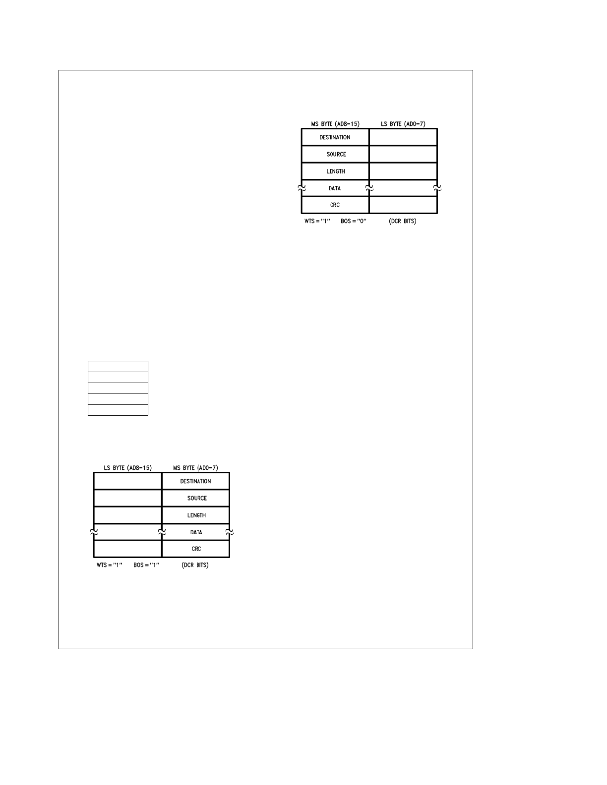
11.0 Initialization Procedures
(Continued)
Before receiving packets, the user must specify the location
of the Receive Buffer Ring. This is programmed in the Page
Start and Page Stop Registers. In addition, the Boundary
and Current Page Registers must be initialized to the value
of the Page Start Register. These registers will be modified
during reception of packets.
12.0 Loopback Diagnostics
Three forms of local loopback are provided on the NIC. The
user has the ability to loopback through the deserializer on
the DP8390D NIC, through the DP8391 SNI, and to the coax
to check the link through the transceiver circuitry. Because
of the half duplex architecture of the NIC, loopback
testing is a special mode of operation with the follow-
ing restrictions:
Restrictions During Loopback
The FIFO is split into two halves, one used for transmission
the other for reception. Only 8-bit fields can be fetched from
memory so two tests are required for 16-bit systems to veri-
fy integrity of the entire data path. During loopback the maxi-
mum latency from the assertion of BREQ to BACK is 2.0 ms.
Systems that wish to use the loopback test yet do not meet
this latency can limit the loopback packet to 7 bytes without
experiencing underflow. Only the last 8 bytes of the loop-
back packet are retained in the FIFO. The last 8 bytes can
be read through the FIFO register which will advance
through the FIFO to allow reading the receive packet se-
quentially.
DESTINATION ADDRESS
e
(6 bytes) Station Physical Address
SOURCE ADDRESS
l
LENGTH
2 bytes
DATA
e
46 to 1500 bytes
CRC
Appended by NIC if CRC e ‘‘0’’ in TCR
When in word-wide mode with Byte Order Select set, the
loopback packet must be assembled in the even byte loca-
tions as shown below. (The loopback only operates with
byte wide transfers.)
TL/F/8582 – 15
When in word-wide mode with Byte Order Select low, the
following format must be used for the loopback packet.
TL/F/8582 – 16
Note:
When using loopback in word mode 2n bytes must be programmed in
TBCR0, 1. Where n e actual number of bytes assembled in even or
odd location.
To initiate a loopback the user first assembles the loopback
packet then selects the type of loopback using the Transmit
Configuration register bits LB0, LB1. The transmit configura-
tion register must also be set to enable or disable CRC gen-
eration during transmission. The user then issues a normal
transmit command to send the packet. During loopback the
receiver checks for an address match and if CRC bit in the
TCR is set, the receiver will also check the CRC. The last 8
bytes of the loopback packet are buffered and can be read
out of the FIFO using the FIFO read port.
Loopback Modes
MODE 1: Loopback Through the Controller (LB1
e
0, LB0
e
1).
If the loopback is through the NIC then the serializer is sim-
ply linked to the deserializer and the receive clock is derived
from the transmit clock.
MODE 2: Loopback Through the SNI (LB1
e
1, LB0
e
0).
If the loopback is to be performed through the SNI, the NIC
provides a control (LPBK) that forces the SNI to loopback
all signals.
MODE 3: Loopback to Coax (LB1
e
1, LB0
e
1).
Packets can be transmitted to the coax in loopback mode to
check all of the transmit and receive paths and the coax
itself.
Note:
In MODE 1, CRS and COL lines are not indicated in any status regis-
ter, but the NIC will still defer if these lines are active. In MODE 2,
COL is masked and in MODE 3 CRS and COL are not masked. It is
not possible to go directly between the loopback modes, it is neces-
sary to return to normal operation (00H) when changing modes.
Reading the Loopback Packet
The last eight bytes of a received packet can be examined
by 8 consecutive reads of the FIFO register. The FIFO
pointer is incremented after the rising edge of the CPU’s
read strobe by internally synchronizing and advancing the
pointer. This may take up to four bus clock cycles, if the
pointer has not been incremented by the time the CPU
reads the FIFO register again, the NIC will insert wait states
Note:
The FIFO may only be read during Loopback. Reading the FIFO at
any other time will cause the NIC to malfunction.
30
12.0 Loopback Diagnostics
(Continued)
Alignment of the Received Packet in the FIFO
Reception of the packet in the FIFO begins at location zero,
after the FIFO pointer reaches the last location in the FIFO,
the pointer wraps to the top of the FIFO overwriting the
previously received data. This process continues until the
last byte is received. The NIC then appends the received
byte count in the next two locations of the FIFO. The con-
tents of the Upper Byte Count are also copied to the next
FIFO location. The number of bytes used in the loopback
packet determines the alignment of the packet in the FIFO.
The alignment for a 64-byte packet is shown below.
FIFO
FIFO
LOCATION
CONTENTS
0
LOWER BYTE COUNT
x
First Byte Read
1
UPPER BYTE COUNT
x
Second Byte Read
2
UPPER BYTE COUNT
#
3
LAST BYTE
#
4
CRC1
#
5
CRC2
#
6
CRC3
#
7
CRC4
x
Last Byte Read
For the following alignment in the FIFO the packet length
should be (N
c
8)
a
5 Bytes. Note that if the CRC bit in the
TCR is set, CRC will not be appended by the transmitter. If
the CRC is appended by the transmitter, the last four bytes,
bytes N-3 to N, correspond to the CRC.
FIFO
FIFO
LOCATION
CONTENTS
0
BYTE N-4
x
First Byte Read
1
BYTE N-3 (CRC1)
AR
Second Byte Read
2
BYTE N-2 (CRC2)
#
3
BYTE N-1 (CRC3)
#
4
BYTE N (CRC4)
#
5
LOWER BYTE COUNT
#
6
UPPER BYTE COUNT
x
Last Byte Read
7
UPPER BYTE COUNT
LOOPBACK TESTS
Loopback capabilities are provided to allow certain tests to
be performed to validate operation of the DP8390D NIC pri-
or to transmitting and receiving packets on a live network.
Typically these tests may be performed during power up of
a node. The diagnostic provides support to verify the follow-
ing:
1) Verify integrity of data path. Received data is checked
against transmitted data.
2) Verify CRC logic’s capability to generate good CRC on
transmit, verify CRC on receive (good or bad CRC).
3) Verify that the Address Recognition Logic can
a) Recognize address match packets
b) Reject packets that fail to match an address
LOOPBACK OPERATION IN THE NIC
Loopback is a modified form of transmission using only half
of the FIFO. This places certain restrictions on the use of
loopback testing. When loopback mode is selected in the
TCR, the FIFO is split. A packet should be assembled in
memory with programming of TPSR and TBCR0,TBCR1
registers. When the transmit command is issued the follow-
ing operations occur:
Transmitter Actions
1) Data is transferred from memory by the DMA until the
FIFO is filled. For each transfer TBCR0 and TBCR1 are
decremented. (Subsequent burst transfers are initiated
when the number of bytes in the FIFO drops below the
programmed threshold.)
2) The NIC generates 56 bits of preamble followed by an
8-bit synch pattern.
3) Data transferred from FIFO to serializer.
4) If CRC
e
1 in TCR, no CRC calculated by NIC, the last
byte transmitted is the last byte from the FIFO (Allows
software CRC to be appended). If CRC
e
0, NIC calcu-
lates and appends four bytes of CRC.
5) At end of Transmission PTX bit set in ISR.
Receiver Actions
1) Wait for synch, all preamble stripped.
2) Store packet in FIFO, increment receive byte count for
each incoming byte.
3) If CRC
e
0 in TCR, receiver checks incoming packet for
CRC errors. If CRC
e
1 in TCR, receiver does not check
CRC errors, CRC error bit always set in RSR (for address
matching packets).
4) At end of receive, receive byte count written into FIFO,
receive status register is updated. The PRX bit is typically
set in the RSR even if the address does not match. If
CRC errors are forced, the packet must match the ad-
dress filters in order for the CRC error bit in the RS to be
set.
EXAMPLES
The following examples show what results can be expected
from a properly operating NIC during loopback. The restric-
tions and results of each type of loopback are listed for
reference. The loopback tests are divided into two sets of
tests. One to verify the data path, CRC generation and byte
count through all three paths. The second set of tests uses
internal loopback to verify the receiver’s CRC checking and
address recognition. For all of the tests the DCR was pro-
grammed to 40h.
PATH
TCR
RCR
TSR
RSR
ISR
NIC Internal
02
00
53(1)
02(2)
02(3)
Note 1:
Since carrier sense and collision detect inputs are blocked during
internal loopback, carrier and CD heartbeat are not seen and the CRS and
CDH bits are set.
Note 2:
CRC errors are always indicated by receiver if CRC is appended by
the transmitter.
Note 3:
Only the PTX bit in the ISR is set, the PRX bit is only set if status is
written to memory. In loopback this action does not occur and the PRX bit
remains 0 for all loopback modes.
Note 4:
All values are hex.
31
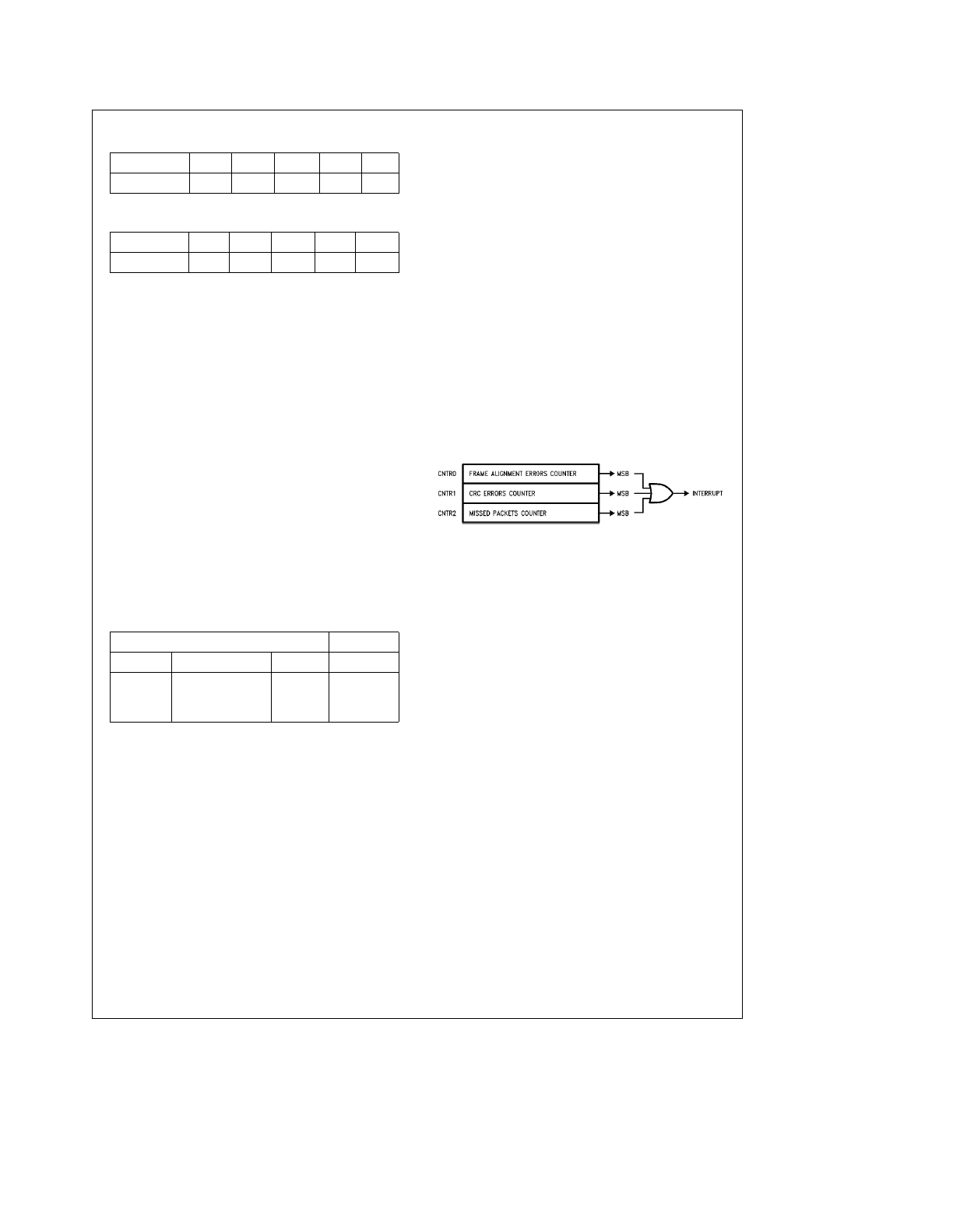
12.0 Loopback Diagnostics
(Continued)
PATH
TCR
RCR
TSR
RSR
ISR
NIC External
04
00
43(1)
02
02
Note 1:
CDH is set, CRS is not set since it is generated by the external
encoder/decoder.
PATH
TCR
RCR
TSR
RSR
ISR
NIC External
06
00
03(1)
02
02(2)
Note 1:
CDH and CRS should not be set. The TSR however, could also
contain 01H,03H,07H and a variety of other values depending on whether
collisions were encountered or the packet was deferred.
Note 2.
Will contain 08H if packet is not transmittable.
Note 3:
During external loopback the NIC is now exposed to network traffic,
it is therefore possible for the contents of both the Receive portion of the
FIFO and the RSR to be corrupted by any other packet on the network. Thus
in a live network the contents of the FIFO and RSR should not be depended
on. The NIC will still abide by the standard CSMA/CD protocol in external
loopback mode. (i.e. The network will not be disturbed by the loopback
packet).
Note 4:
All values are hex.
CRC AND ADDRESS RECOGNITION
The next three tests exercise the address recognition logic
and CRC. These tests should be performed using internal
loopback only so that the NIC is isolated from interference
from the network. These tests also require the capability to
generate CRC in software.
The address recognition logic cannot be directly tested. The
CRC and FAE bits in the RSR are only set if the address of
the packet matches the address filters. If errors are expect-
ed to be set and they are not set, the packet has been
rejected on the basis of an address mismatch. The following
sequence of packets will test the address recognition logic.
The DCR should be set to 40H, the TCR should be set to
03H with a software generated CRC.
Packet Contents
Results
Test
Address
CRC
RSR
Test A
Matching
Good
01(1)
Test B
Matching
Bad
02(2)
Test C
Non-Matching
Bad
01
Note 1:
Status will read 21H if multicast address used.
Note 2:
Status will read 22H if multicast address used.
Note 3:
In test A, the RSR is set up. In test B the address is found to match
since the CRC is flagged as bad. Test C proves that the address recognition
logic can distinguish a bad address and does not notify the RSR of the bad
CRC. The receiving CRC is proven to work in test A and test B.
Note 4:
All values are hex.
NETWORK MANAGEMENT FUNCTIONS
Network management capabilities are required for mainte-
nance and planning of a local area network. The NIC sup-
ports the minimum requirement for network management in
hardware, the remaining requirements can be met with soft-
ware counts. There are three events that software alone
can not track during reception of packets: CRC errors,
Frame Alignment errors, and missed packets.
Since errored packets can be rejected, the status associat-
ed with these packets is lost unless the CPU can access the
Receive Status Register before the next packet arrives. In
situations where another packet arrives very quickly, the
CPU may have no opportunity to do this. The NIC counts
the number of packets with CRC errors and Frame Align-
ment errors. 8-bit counters have been selected to reduce
overhead. The counters will generate interrupts whenever
their MSBs are set so that a software routine can accumu-
late the network statistics and reset the counters before
overflow occurs. The counters are sticky so that when they
reach a count of 192 (C0H) counting is halted. An additional
counter is provided to count the number of packets NIC
misses due to buffer overflow or being offline.
The structure of the counters is shown below:
TL/F/8582 – 63
Additional information required for network management is
available in the Receive and Transmit Status Registers.
Transmit status is available after each transmission for infor-
mation regarding events during transmission.
Typically, the following statistics might be gathered in soft-
ware:
Traffic:
Frames Sent OK
Frames Received OK
Multicast Frames Received
Packets Lost Due to Lack of Resources
Retries/Packet
Errors:
CRC Errors
Alignment Errors
Excessive Collisions
Packet with Length Errors
Heartbeat Failure
32
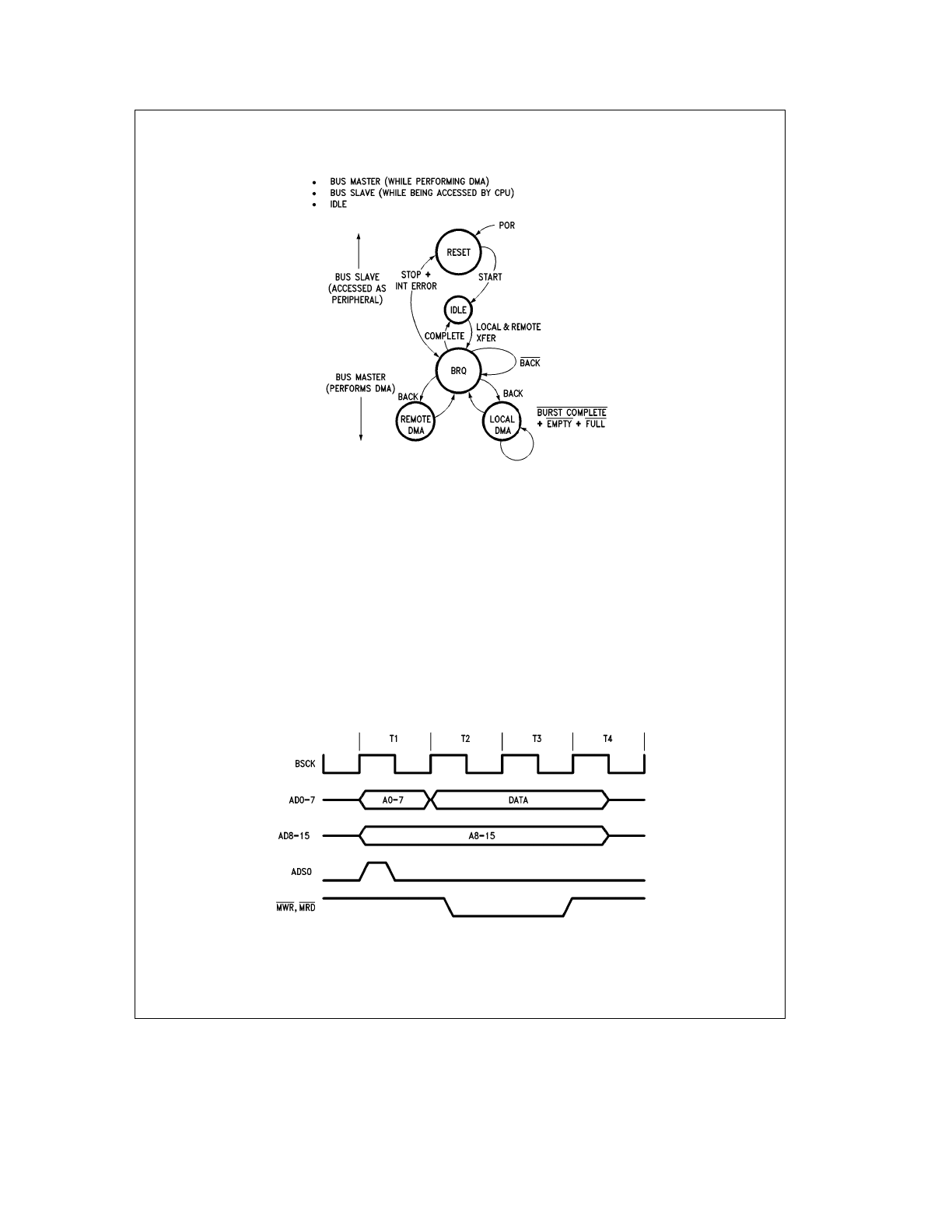
13.0 Bus Arbitration and Timing
The NIC operates in three possible modes:
TL/F/8582 – 64
Upon power-up the NIC is in an indeterminant state. After
receiving a Hardware Reset the NIC comes up as a slave in
the Reset State. The receiver and transmitter are both dis-
abled in this state. The reset state can be reentered under
three conditions, soft reset (Stop Command), hard reset
(RESET input) or an error that shuts down the receiver or
transmitter (FIFO underflow or overflow). After initialization
of registers, the NIC is issued a Start command and the NIC
enters Idle state. Until the DMA is required the NIC remains
in an idle state. The idle state is exited by a request from the
FIFO in the case of receive or transmit, or from the Remote/
DMA in the case of Remote DMA operation. After acquiring
the bus in a BREQ/BACK handshake the Remote or Local
DMA transfer is completed and the NIC reenters the idle
state.
DMA TRANSFERS TIMING
The DMA can be programmed for the following types of
transfers:
16-Bit Address, 8-bit Data Transfer
16-Bit Address, 16-bit Data Transfer
32-Bit Address, 8-bit Data Transfer
32-Bit Address, 16-bit Data Transfer
All DMA transfers use BSCK for timing. 16-Bit Address
modes require 4 BSCK cycles as shown below:
16-Bit Address, 8-Bit Data
TL/F/8582 – 65
33
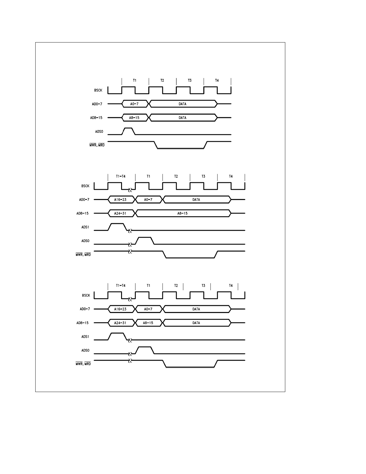
13.0 Bus Arbitration and Timing
(Continued)
16-Bit Address, 16-Bit Data
TL/F/8582 – 66
32-Bit Address, 8-Bit Data
TL/F/8582 – 67
32-Bit Address, 16-Bit Data
TL/F/8582 – 68
Note:
In 32-bit address mode, ADS1 is at TRI-STATE after the first T1–T4 states; thus, a 4.7k pull-down resistor is required for 32-bit address mode.
34
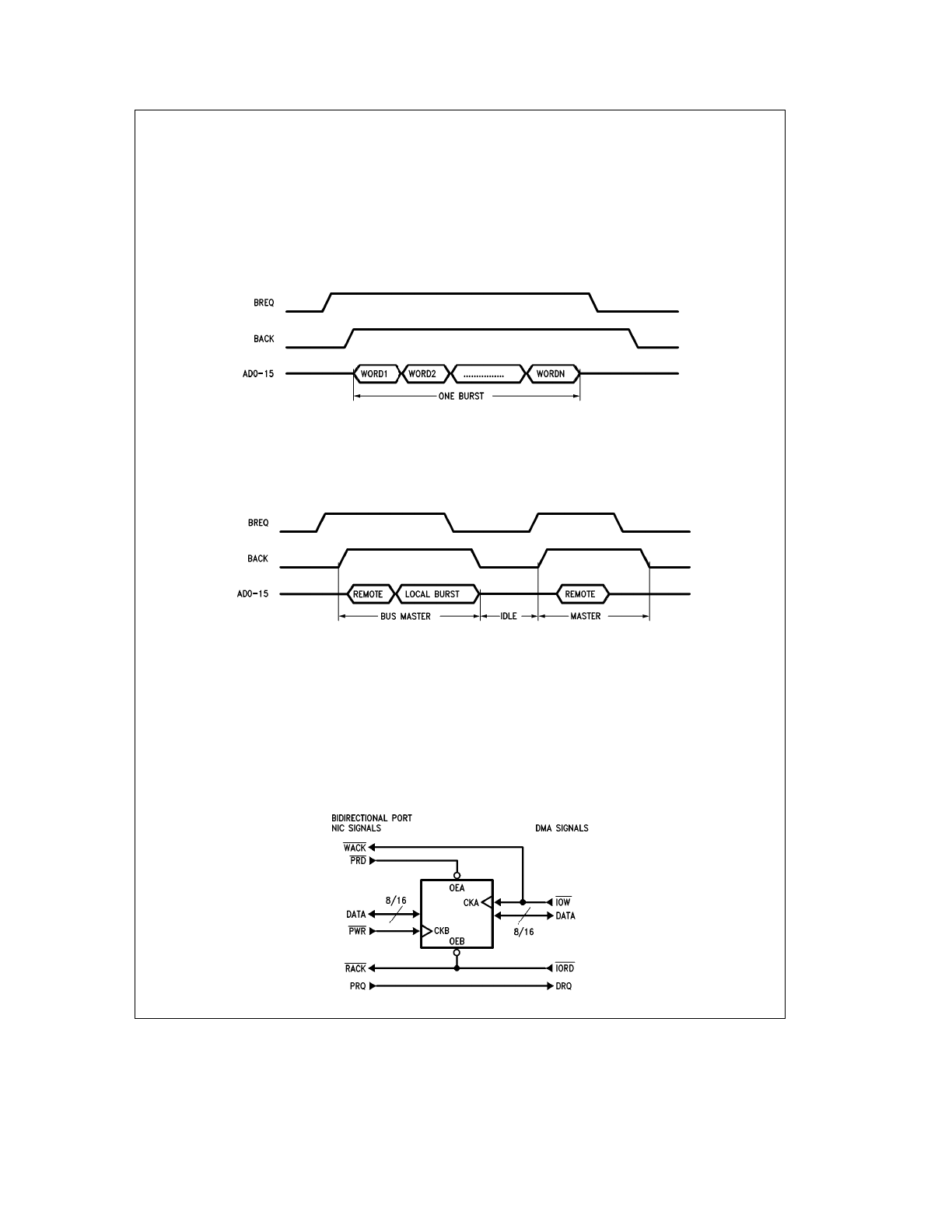
13.0 Bus Arbitration and Timing
(Continued)
When in 32-bit mode four additional BSCK cycles are re-
quired per burst. The first bus cycle (T1
Ê
– T4
Ê
) of each burst
is used to output the upper 16-bit addresses. This 16-bit
address is programmed in RSAR0 and RSAR1 and points to
a 64k page of system memory. All transmitted or received
packets are constrained to reside within this 64k page.
FIFO BURST CONTROL
All Local DMA transfers are burst transfers, once the DMA
requests the bus and the bus is acknowledged, the DMA will
transfer an exact burst of bytes programmed in the Data
Configuration Register (DCR) then relinquish the bus. If
there are remaining bytes in the FIFO the next burst will not
be initiated until the FIFO threshold is exceeded. If BACK is
removed during the transfer, the burst transfer will be abort-
ed. (DROPPING BACK DURING A DMA CYCLE IS NOT
RECOMMENDED.)
TL/F/8582 – 69
where N e 1, 2, 4, or 6 Words or N e 2, 4, 8, or 12 Bytes when in byte mode
INTERLEAVED LOCAL OPERATION
If a remote DMA transfer is initiated or in progress when a
packet is being received or transmitted, the Remote DMA
transfer will be interrupted for higher priority Local DMA
transfers. When the Local DMA transfer is completed the
Remote DMA will rearbitrate for the bus and continue its
transfers. This is illustrated below:
TL/F/8582 – 70
Note that if the FIFO requires service while a remote DMA is
in progress, BREQ is not dropped and the Local DMA burst
is appended to the Remote Transfer. When switching from
a local transfer to a remote transfer, however, BREQ is
dropped and raised again. This allows the CPU or other
devices to fairly contend for the bus.
REMOTE DMA-BIDIRECTIONAL PORT CONTROL
The Remote DMA transfers data between the local buffer
memory and a bidirectional port (memory to I/O transfer).
This transfer is arbited on a byte by byte basis versus the
burst transfer used for Local DMA transfers. This bidirec-
tional port is also read/written by the host. All transfers
through this port are asynchronous. At any one time trans-
fers are limited to one direction, either from the port to local
buffer memory (Remote Write) or from local buffer memory
to the port (Remote Read).
Bus Handshake Signals for Remote DMA Transfers
TL/F/8582 – 71
35
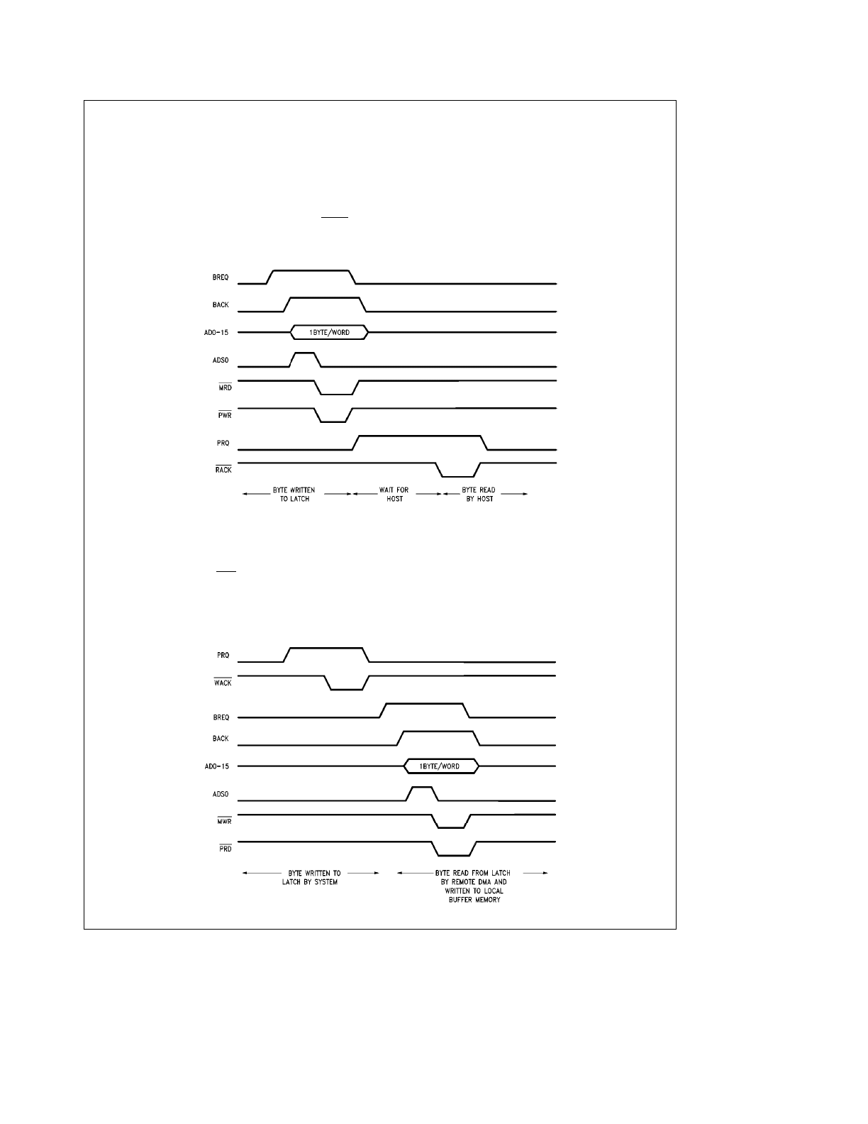
13.0 Bus Arbitration and Timing
(Continued)
REMOTE READ TIMING
1) The DMA reads byte/word from local buffer memory and
writes byte/word into latch, increments the DMA address
and decrements the byte count (RBCR0,1).
2) A Request Line (PRQ) is asserted to inform the system
that a byte is available.
3) The system reads the port, the read strobe (RACK) is
used as an acknowledge by the Remote DMA and it goes
back to step 1.
Steps 1 – 3 are repeated until the remote DMA is com-
plete.
Note that in order for the Remote DMA to transfer a byte
from memory to the latch, it must arbitrate access to the
local bus via a BREQ, BACK handshake. After each byte or
word is transferred to the latch, BREQ is dropped. If a Local
DMA is in progress, the Remote DMA is held off until the
local DMA is complete.
TL/F/8582 – 72
REMOTE WRITE TIMING
A Remote Write operation transfers data from the I/O port
to the local buffer RAM. The NIC initiates a transfer by re-
questing a byte/word via the PRQ. The system transfers a
byte/word to the latch via IOW, this write strobe is detected
by the NIC and PRQ is removed. By removing the PRQ, the
Remote DMA holds off further transfers into the latch until
the current byte/word has been transferred from the latch,
PRQ is reasserted and the next transfer can begin.
1) NIC asserts PRQ. System writes byte/word into latch.
NIC removes PRQ.
2) Remote DMA reads contents of port and writes
byte/word to local buffer memory, increments address
and decrements byte count (RBCR0,1).
3) Go back to step 1.
Steps 1 – 3 are repeated until the remote DMA is com-
plete.
TL/F/8582 – 73
36
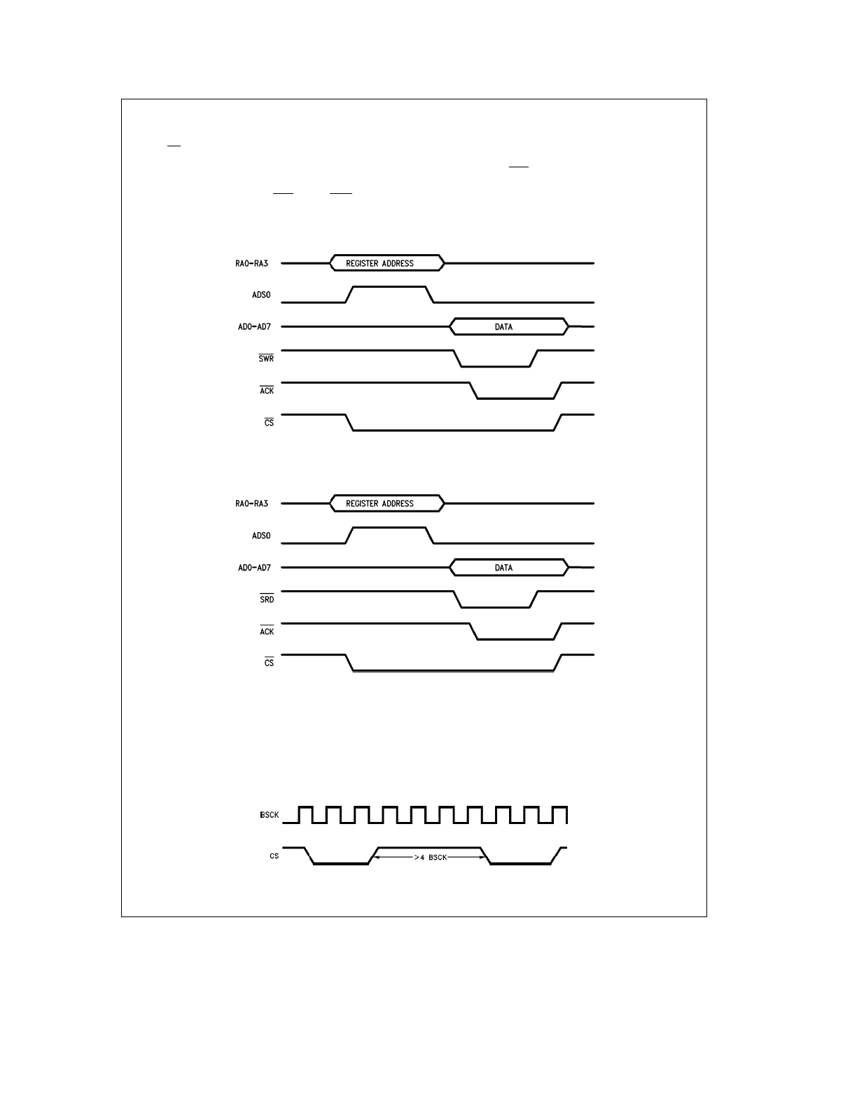
13.0 Bus Arbitration and Timing
(Continued)
SLAVE MODE TIMING
When CS is low, the NIC becomes a bus slave. The CPU
can then read or write any internal registers. All register
access is byte wide. The timing for register access is shown
below. The host CPU accesses internal registers with four
address
lines,
RA0 – RA3,
SRD
and
SWR
strobes.
ADS0 is used to latch the address when interfacing to a
multiplexed, address data bus. Since the NIC may be a local
bus master when the host CPU attempts to read or write to
the controller, an ACK line is used to hold off the CPU until
the NIC leaves master mode. Some number of BSCK cycles
is also required to allow the NIC to synchronize to the read
or write cycle.
Write to Register
TL/F/8582 – 74
Read from Register
TL/F/8582 – 75
TIME BETWEEN CHIP SELECTS
The NIC requires that successive chip selects be no closer
than 4 bus clocks (BSCK) together, below. If the condition is
violated, the NIC may glitch/ACK. CPUs that operate from
pipelined instructions (i.e. 386) or have a cache (i.e.
486) can execute consecutive I/O cycles very quickly. The
solution is to delay the execution of consecutive I/O cycles
by either breaking the pipeline or forcing the CPU to access
outisde it’s cache.
Time between Chip Selects
TL/F/8582 – A1
37

14.0 Preliminary Electrical Characteristics
Absolute Maximum Ratings
If Military/Aerospace specified devices are required,
please contact the National Semiconductor Sales
Office/Distributors for availability and specifications.
Supply Voltage (V
CC
)
b
0.5V to
a
7.0V
DC Input Voltage (V
IN
)
b
0.5V to V
CC
a
0.5V
DC Output Voltage (V
OUT
)
b
0.5V to V
CC
a
0.5V
Storage Temperature Range (T
STG
)
b
65
§
C to
a
150
§
C
Power Dissipation (PD)
500 mW
Lead Temp. (TL) (Soldering, 10 sec.)
260
§
C
ESD rating (R
ZAP
e
1.5k, C
ZAP
e
120 pF)
1600V
Preliminary DC Specifications
T
A
e
0
§
C to 70
§
C, V
CC
e
5V
g
5%, unless otherwise specified
Symbol
Parameter
Conditions
Min
Max
Units
V
OH
Minimum High Level Output Voltage
I
OH
e b
20 mA
V
CC
b
0.1
V
(Notes 1, 4)
I
OH
e b
2.0 mA
3.5
V
V
OL
Minimum Low Level Output Voltage
I
OL
e
20 mA
0.1
V
(Notes 1, 4)
I
OL
e
2.0 mA
0.4
V
V
IH
Minimum High Level Input Voltage
2.0
V
(Note 2)
V
IH2
Minimum High Level Input Voltage
2.7
V
for RACK, WACK (Note 2)
V
IL
Minimum Low Level Input Voltage
0.8
V
(Note 2)
V
IL2
Minimum Low Level Input Voltage
0.6
V
For RACK, WACK (Note 2)
I
IN
Input Current
V
I
e
V
CC
or GND
b
1.0
a
1.0
m
A
I
OZ
Maximum TRI-STATE
V
OUT
e
V
CC
or GND
b
10
a
10
m
A
Output Leakage Current
I
CC
Average Supply Current
TXCK
e
10 MHz
(Note 3)
RXCK
e
10 MHz
BSCK
e
20 MHz
40
mA
I
OUT
e
0 mA
V
IN
e
V
CC
or GND
Note 1:
These levels are tested dynamically using a limited amount of functional test patterns, please refer to AC Test Load.
Note 2:
Limited functional test patterns are performed at these input levels. The majority of functional tests are performed at levels of 0V and 3V.
Note 3:
This is measured with a 0.1 mF bypass capacitor between V
CC
and GND.
Note 4:
The low drive CMOS compatible V
OH
and V
OL
limits are not tested directly. Detailed device characterization validates that this specification can be
guaranteed by testing the high drive TTL compatible V
OL
and V
OH
specification.
38
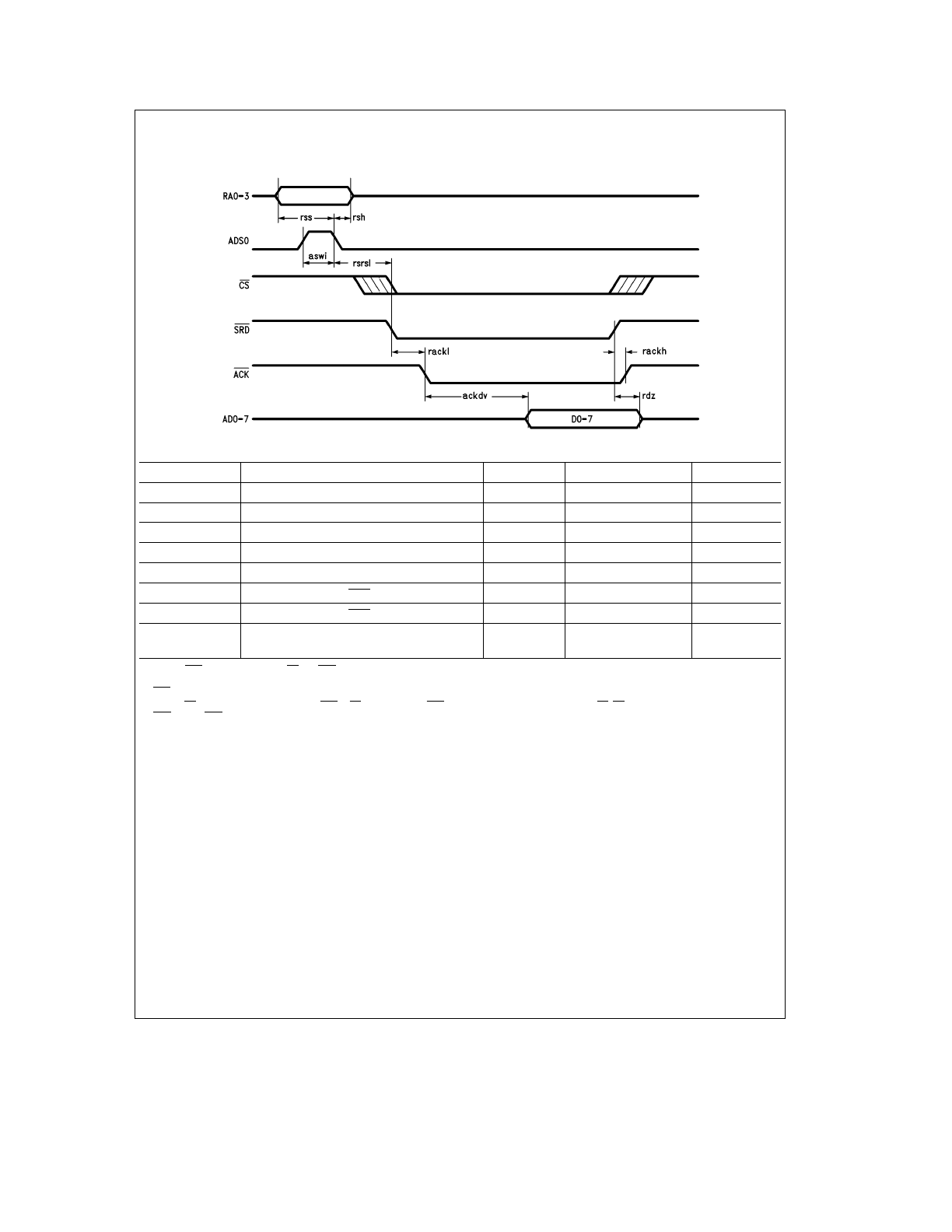
15.0 Switching Characteristics
AC Specs DP8390D Note: All Timing is Preliminary
Register Read (Latched Using ADS0)
TL/F/8582 – 76
Symbol
Parameter
Min
Max
Units
rss
Register Select Setup to ADS0 Low
10
ns
rsh
Register Select Hold from ADS0 Low
13
ns
aswi
Address Strobe Width In
15
ns
ackdv
Acknowledge Low to Data Valid
55
ns
rdz
Read Strobe to Data TRI-STATE
15
70
ns
rackl
Read Strobe to ACK Low (Notes 1, 3)
n*bcyc
a
30
ns
rackh
Read Strobe to ACK High
30
ns
rsrsl
Register Select to Slave Read Low,
10
ns
Latched RS0 – 3 (Note 2)
Note 1:
ACK is not generated until CS and SRD are low and the NIC has synchronized to the register access. The NIC will insert an integral number of Bus Clock
cycles until it is synchronized. In Dual Bus systems additional cycles will be used for a local or remote DMA to complete. Wait states must be issued to the CPU until
ACK is asserted low.
Note 2:
CS may be asserted before or after SRD. If CS is asserted after SRD, rackl is referenced from falling edge of CS. CS can be de-asserted concurrently with
SRD or after SRD is de-asserted.
Note 3:
These limits include the RC delay inherent in our test method. These signals typically turn off within 15 ns, enabling other devices to drive these lines with
no contention.
39
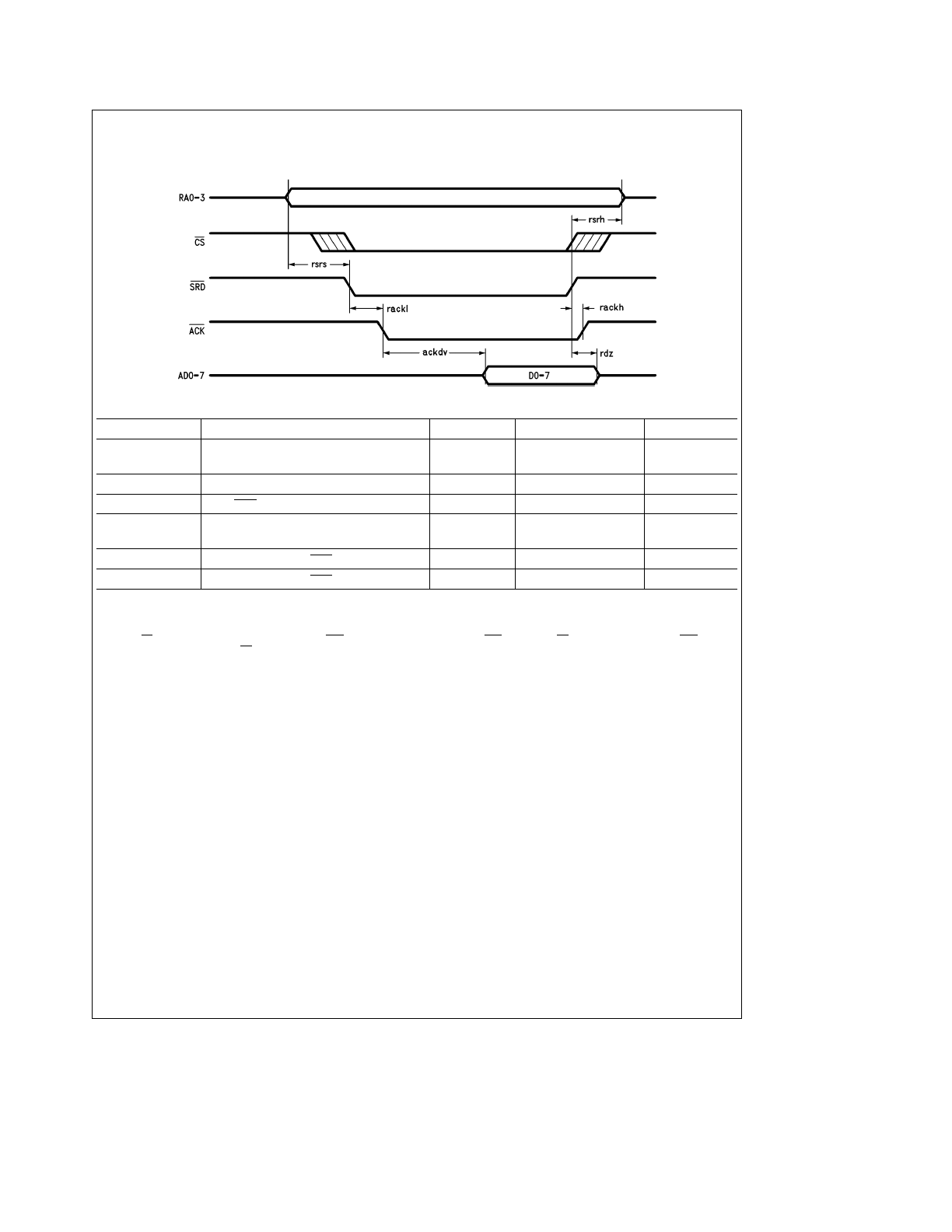
15.0 Switching Characteristics
(Continued)
Register Read (Non Latched, ADS0
e
1)
TL/F/8582 – 77
Symbol
Parameter
Min
Max
Units
rsrs
Register Select to Read Setup
10
ns
(Notes 1, 3)
rsrh
Register Select Hold from Read
0
ns
ackdv
ACK Low to Valid Data
55
ns
rdz
Read Strobe to Data TRI-STATE
15
70
ns
(Note 2)
rackl
Read Strobe to ACK Low (Note 3)
n*bcyc
a
30
ns
rackh
Read Strobe to ACK High
30
ns
Note 1:
rsrs includes flow-through time of latch.
Note 2:
These limits include the RC delay inherent in our test method. These signals typically turn off within 15 ns enabling other devices to drive these lines with
no contention.
Note 3:
CS may be asserted before or after RA0–3, and SRD, since address decode begins when ACK is asserted. If CS is asserted after RA0-3, and SRD, rack1
is referenced from falling edge of CS.
40
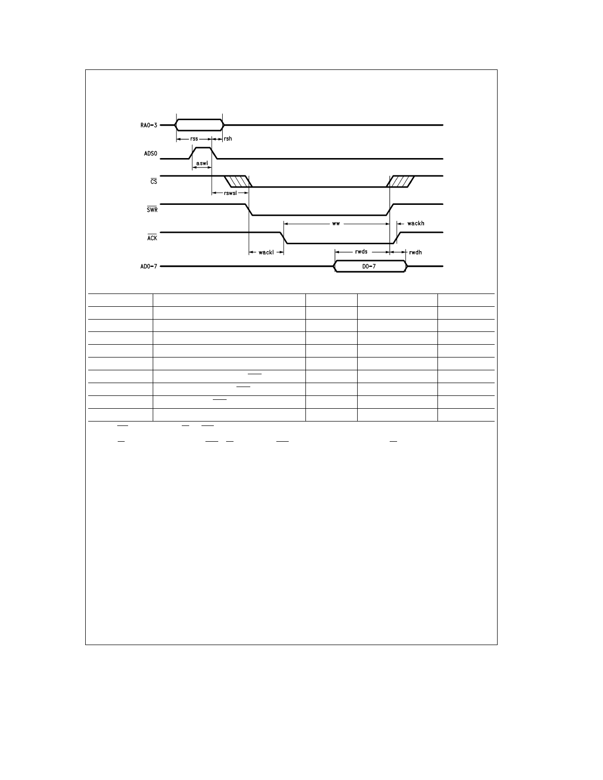
15.0 Switching Characteristics
(Continued)
Register Write (Latched Using ADS0)
TL/F/8582 – 78
Symbol
Parameter
Min
Max
Units
rss
Register Select Setup to ADS0 Low
10
ns
rsh
Register Select Hold from ADS0 Low
17
ns
aswi
Address Strobe Width In
15
ns
rwds
Register Write Data Setup
20
ns
rwdh
Register Write Data Hold
21
ns
ww
Write Strobe Width from ACK
50
ns
wackh
Write Strobe High to ACK High
30
ns
wackl
Write Low to ACK Low (Notes 1, 2)
n*bcyc
a
30
ns
rswsl
Register Select to Write Strobe Low
10
ns
Note 1:
ACK is not generated until CS and SWR are low and the NIC has synchronized to the register access. In Dual Bus Systems additional cycles will be used
for a local DMA or Remote DMA to complete.
Note 2:
CS may be asserted before or after SWR. If CS is asserted after SWR, wackl is referenced from falling edge of CS.
41
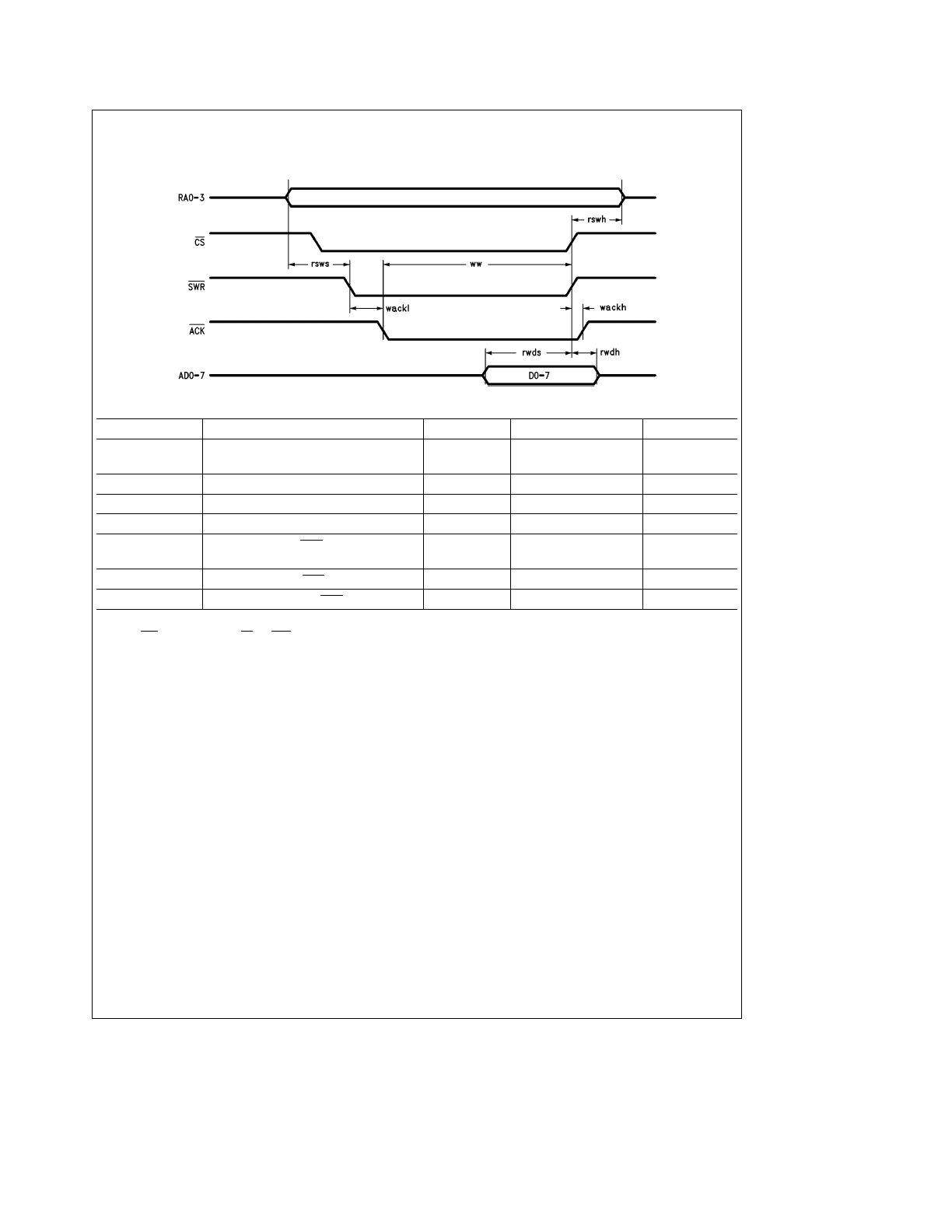
15.0 Switching Characteristics
(Continued)
Register Write (Non Latched, ADS0
e
1)
TL/F/8582 – 79
Symbol
Parameter
Min
Max
Units
rsws
Register Select to Write Setup
15
ns
(Note 1)
rswh
Register Select Hold from Write
0
ns
rwds
Register Write Data Setup
20
ns
rwdh
Register Write Data Hold
21
ns
wackl
Write Low to ACK Low
n*bcyc
a
30
ns
(Note 2)
wackh
Write High to ACK High
30
ns
ww
Write Width from ACK
50
ns
Note 1:
Assumes ADS0 is high when RA0–3 changing.
Note 2:
ACK is not generated until CS and SWR are low and the NIC has synchronized to the register access. In Dual Bus systems additional cycles will be used for
a local DMA or remote DMA to complete.
42
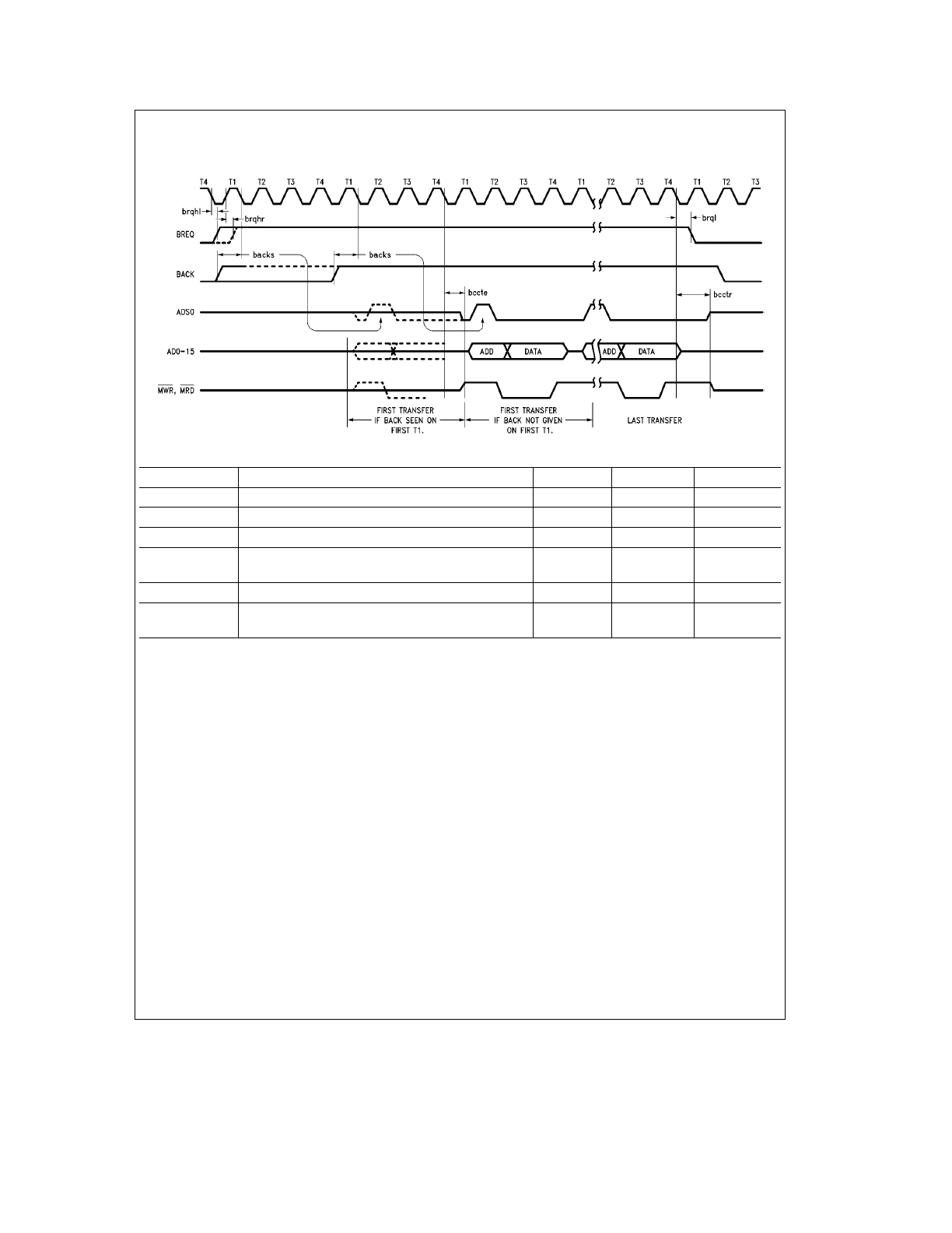
15.0 Switching Characteristics
(Continued)
DMA Control, Bus Arbitration
TL/F/8582 – 80
Symbol
Parameter
Min
Max
Units
brqhl
Bus Clock to Bus Request High for Local DMA
43
ns
brqhr
Bus Clock to Bus Request High for Remote DMA
38
ns
brql
Bus Request Low from Bus Clock
55
ns
backs
Acknowledge Setup to Bus Clock
2
ns
(Note 1)
bccte
Bus Clock to Control Enable
60
ns
bcctr
Bus Clock to Control Release
70
ns
(Notes 2, 3)
Note 1:
BACK must be setup before T1 after BREQ is asserted. Missed setup will slip the beginning of the DMA by four bus clocks. The Bus Latency will influence
the allowable FIFO threshold and transfer mode (empty/fill vs exact burst transfer).
Note 2:
During remote DMA transfers only, a single bus transfer is performed. During local DMA operations burst mode transfers are performed.
Note 3:
These limits include the RC delay inherent in our test method. These signals typically turn off within 15 ns enabling other devices to drive these lines with
no contention.
43
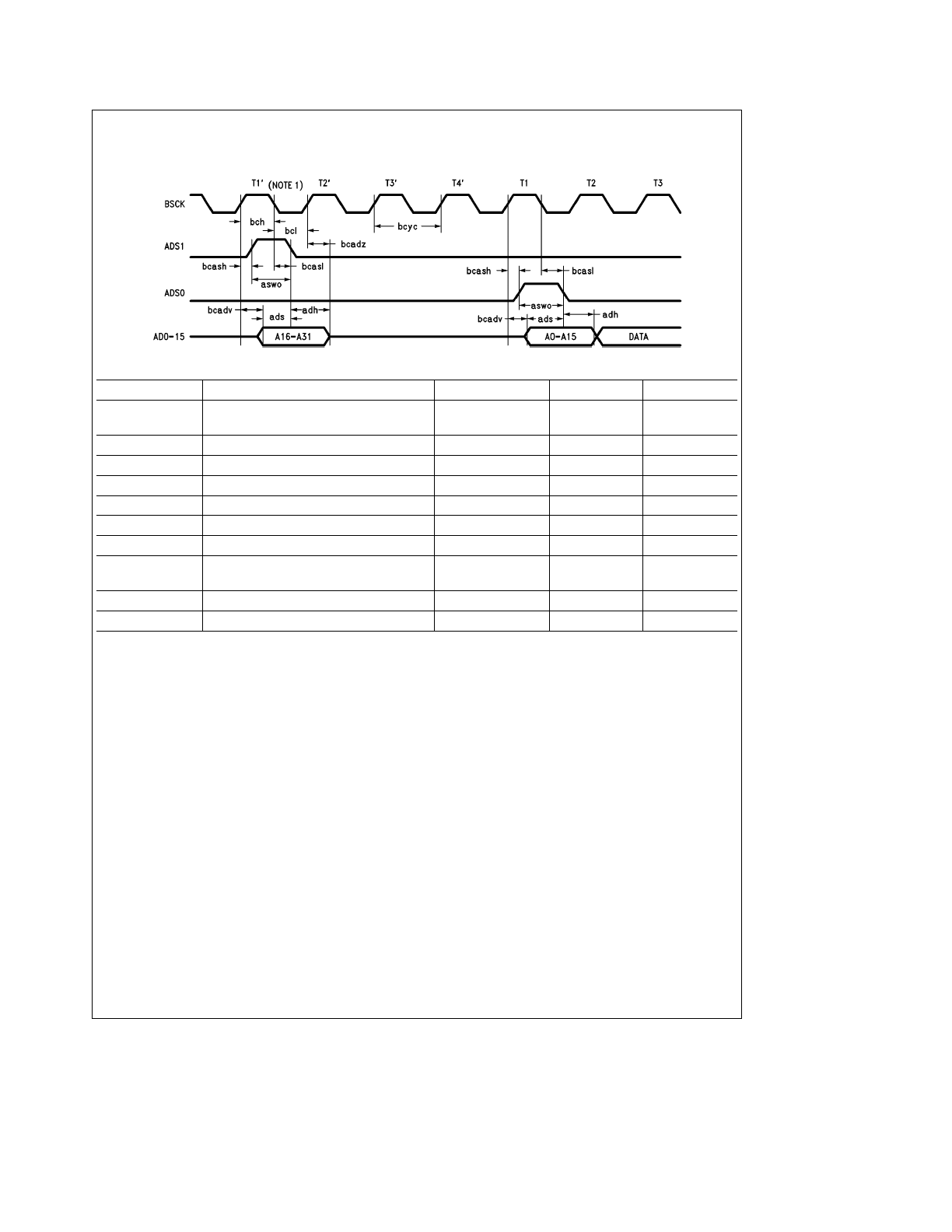
15.0 Switching Characteristics
(Continued)
DMA Address Generation
TL/F/8582 – 81
Symbol
Parameter
Min
Max
Units
bcyc
Bus Clock Cycle Time
50
1000
ns
(Note 2)
bch
Bus Clock High Time
22.5
ns
bcl
Bus Clock Low Time
22.5
ns
bcash
Bus Clock to Address Strobe High
34
ns
bcasl
Bus Clock to Address Strobe Low
44
ns
aswo
Address Strobe Width Out
bch
ns
bcadv
Bus Clock to Address Valid
45
ns
bcadz
Bus Clock to Address TRI-STATE
15
55
ns
(Note 3)
ads
Address Setup to ADS0/1 Low
bch
b
15
ns
adh
Address Hold from ADS0/1 Low
bcl
b
5
ns
Note 1:
Cycles T1’, T2’, T3’, T4’ are only issued for the first transfer in a burst when 32-bit mode has been selected.
Note 2:
The rate of bus clock must be high enough to support transfers to/from the FIFO at a rate greater than the serial network transfers from/to the FIFO.
Note 3:
These limits include the RC delay inherent in our test method. These signals typically turn off within 15 ns, enabling other devices to drive these lines with
no contention.
44
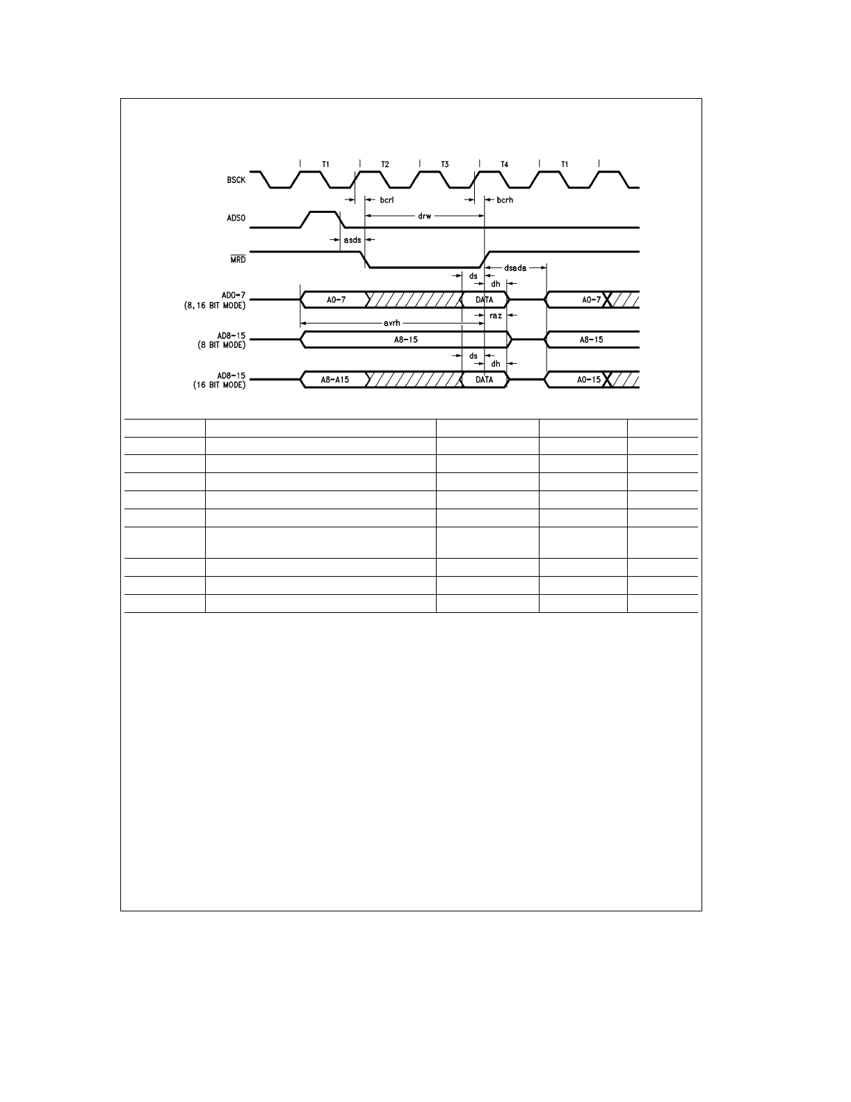
15.0 Switching Characteristics
(Continued)
DMA Memory Read
TL/F/8582 – 82
Symbol
Parameter
Min
Max
Units
bcrl
Bus Clock to Read Strobe Low
43
ns
bcrh
Bus Clock to Read Strobe High
40
ns
ds
Data Setup to Read Strobe High
25
ns
dh
Data Hold from Read Strobe High
0
ns
drw
DMA Read Strobe Width Out
2*bcyc
b
15
ns
raz
Memory Read High to Address TRI-STATE
bch
a
40
ns
(Notes 1, 2)
asds
Address Strobe to Data Strobe
bcl
a
10
ns
dsada
Data Strobe to Address Active
bcyc
b
10
ns
avrh
Address Valid to Read Strobe High
3*bcyc
b
15
ns
Note 1:
During a burst A8–A15 are not TRI-STATE if byte wide transfers are selected. On the last transfer A8–A15 are TRI-STATE as shown above.
Note 2:
These limits include the RC delay inherent in our test method. These signals typically turn off within bch a 15 ns, enabling other devices to drive these
lines with no contention.
45
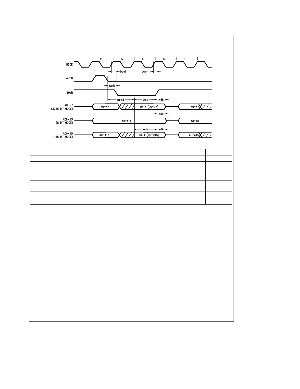
15.0 Switching Characteristics
(Continued)
DMA Memory Write
TL/F/8582 – 83
Symbol
Parameter
Min
Max
Units
bcwl
Bus Clock to Write Strobe Low
40
ns
bcwh
Bus Clock to Write Strobe High
40
ns
wds
Data Setup to WR High
2*bcyc
b
30
ns
wdh
Data Hold from WR Low
bch
a
7
ns
waz
Write Strobe to Address TRI-STATE
bch
a
40
ns
(Notes 1, 2)
asds
Address Strobe to Data Strobe
bcl
a
10
ns
aswd
Address Strobe to Write Data Valid
bcl
a
30
ns
Note 1:
When using byte mode transfers A8–A15 are only TRI-STATE on the last transfer, waz timing is only valid for last transfer in a burst.
Note 2:
These limits include the RC delay inherent in our test method. These signals typically turn off within bch a 15 ns, enabling other devices to drive these
lines with no contention.
46
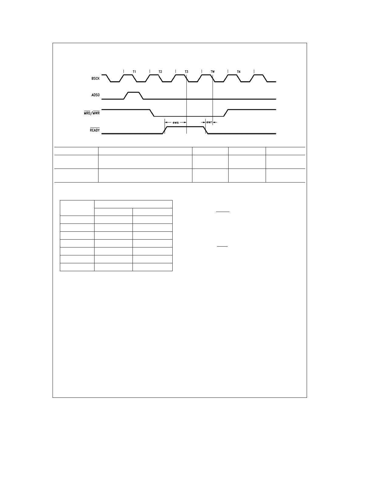
15.0 Switching Characteristics
(Continued)
Wait State Insertion
TL/F/8582 – 45
Symbol
Parameter
Min
Max
Units
ews
External Wait Setup to T3
v
Clock
10
ns
(Note 1)
ewr
External Wait Release Time
15
ns
(Note 1)
Note 1:
The addition of wait states affects the count of deserialized bytes and is limited to a number of bus clock cycles depending on the bus clock and network
rates. The allowable wait states are found in the table below. (Assumes 10 Mbit/sec data rate.)
BSCK (MHz)
Ý
of Wait States
Byte Transfer
Word Transfer
8
0
1
10
0
1
12
1
2
14
1
2
16
1
3
18
2
3
20
2
4
Table assumes 10 MHz network clock.
The number of allowable wait states in byte mode can be calculated using:
Ý
W
(byte mode)
e
#
8 tnw
4.5 tbsck
b
1
J
Ý
W
e
Number of Wait States
tnw
e
Network Clock Period
tbsck
e
BSCK Period
The number of allowable wait states in word mode can be calculated using:
Ý
W
(word mode)
e
#
5 tnw
2 tbsck
b
1
J
47
15.0 Switching Characteristics
(Continued)
Remote DMA (Read, Send Command)
TL/F/8582 – 84
Symbol
Parameter
Min
Max
Units
bpwrl
Bus Clock to Port Write Low
43
ns
bpwrh
Bus Clock to Port Write High
40
ns
prqh
Port Write High to Port
30
ns
Request High (Note 1)
prql
Port Request Low from
45
ns
Read Acknowledge High
rakw
Remote Acknowledge
20
ns
Read Strobe Pulse Width
Note 1:
Start of next transfer is dependent on where RACK is generated relative to BSCK and whether a local DMA is pending.
48
15.0 Switching Characteristics
(Continued)
Remote DMA (Read, Send Command) Recovery Time
TL/F/8582 – 85
Symbol
Parameter
Min
Max
Units
bpwrl
Bus Clock to Port Write Low
43
ns
bpwrh
Bus Clock to Port Write High
40
ns
prqh
Port Write High to Port
30
ns
Request High (Note 1)
prql
Port Request Low from
45
ns
Read Acknowledge High
rakw
Remote Acknowledge
20
ns
Read Strobe Pulse Width
rhpwh
Read Acknowledge High to
Next Port Write Cycle
11
BUSCK
(Notes 2,3,4)
Note 1:
Start of next transfer is dependent on where RACK is generated relative to BSCK and whether a local DMA is pending.
Note 2:
This is not a measured value but guaranteed by design.
Note 3:
RACK must be high for a minimum of 7 BUSCK.
Note 4:
Assumes no local DMA interleave, no CS, and immediate BACK.
49
15.0 Switching Characteristics
(Continued)
Remote DMA (Write Cycle)
TL/F/8582 – 86
Symbol
Parameter
Min
Max
Units
bprqh
Bus Clock to Port Request High
42
ns
(Note 1)
wprql
WACK to Port Request Low
45
ns
wackw
WACK Pulse Width
20
ns
bprdl
Bus Clock to Port Read Low
40
ns
(Note 2)
bprdh
Bus Clock to Port Read High
40
ns
Note 1:
The first port request is issued in response to the remote write command. It is subsequently issued on T1 clock cycles following completion of remote DMA
cycles.
Note 2:
The start of the remote DMA write following WACK is dependent on where WACK is issued relative to BUSCK and whether a local DMA is pending.
50
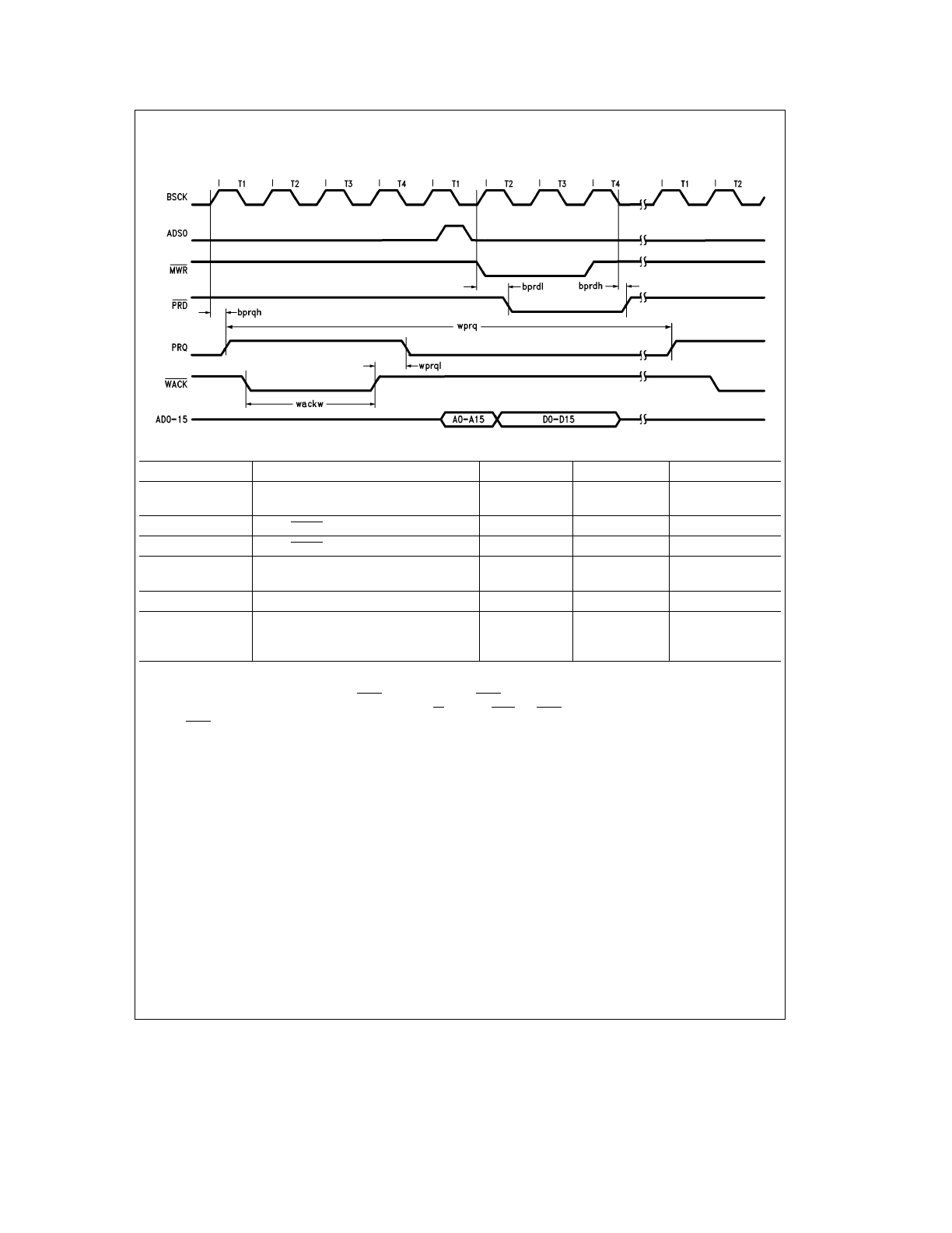
15.0 Switching Characteristics
(Continued)
Remote DMA (Write Cycle) Recovery Time
TL/F/8582 – 87
Symbol
Parameter
Min
Max
Units
bprqh
Bus Clock to Port Request High
40
ns
(Note 1)
wprql
WACK to Port Request Low
45
ns
wackw
WACK Pulse Width
20
ns
bprdl
Bus Clock to Port Read Low
40
ns
(Note 2)
bprdh
Bus Clock to Port Read High
40
ns
wprq
Remote Write Port Request
to Port Request Time
12
BUSCK
(Notes 3,4,5)
Note 1:
The first port request is issued in response to the remote write command. It is subsequently issued on T1 clock cycles following completion of remote DMA
cycles.
Note 2:
The start of the remote DMA write following WACK is dependent on where WACK is issued relative to BUSCK and whether a local DMA is pending.
Note 3:
Assuming wackw
k
1 BUSCK, and no local DMA interleave, no CS, immediate BACK, and WACK goes high before T4.
Note 4:
WACK must be high for a minimum of 7 BUSCK.
Note 5:
This is not a measured value but guaranteed by design.
51
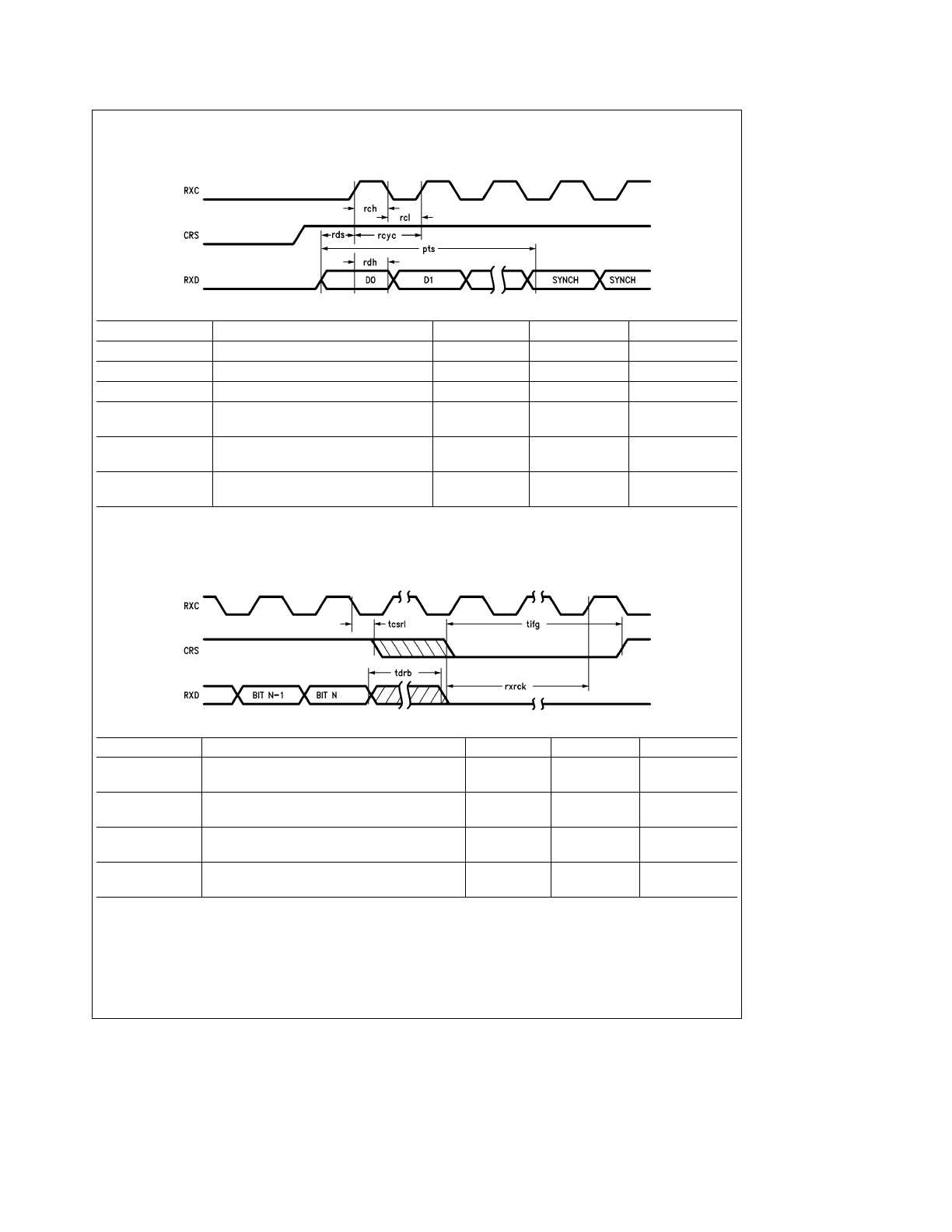
15.0 Switching Characteristics
(Continued)
Serial TimingÐReceive (Beginning of Frame)
TL/F/8582 – 88
Symbol
Parameter
Min
Max
Units
rch
Receive Clock High Time
40
ns
rcl
Receive Clock Low Time
40
ns
rcyc
Receive Clock Cycle Time
80
120
ns
rds
Receive Data Setup Time to
20
ns
Receive Clock High (Note 1)
rdh
Receive Data Hold Time from
17
ns
Receive Clock High
pts
First Preamble Bit to Synch
8
rcyc
(Note 2)
cycles
Note 1:
All bits entering NIC must be properly decoded, if the PLL is still locking, the clock to the NIC should be disabled or CRS delayed. Any two sequential 1 data
bits will be interpreted as Synch.
Note 2:
This is a minimum requirement which allows reception of a packet.
Serial TimingÐReceive (End of Frame)
TL/F/8582 – 89
Symbol
Parameter
Min
Max
Units
rxrck
Minimum Number of Receive Clocks
5
rcyc
after CRS Low (Note 1)
cycles
tdrb
Maximum of Allowed Dribble Bits/Clocks
3
rcyc
(Note 2)
cycles
tifg
Receive Recovery Time
40
rcyc
(Notes 4,5)
cycles
tcrsl
Receive Clock to Carrier Sense Low
0
1
rcyc
(Note 3)
cycles
Note 1:
The NIC requires a minimum number of receive clocks following the de-assertion of carrier sense (CRS). These additional clocks are provided by the
DP8391 SNI. If other decoder/PLLs are being used additional clocks should be provided. Short clocks or glitches are not allowed.
Note 2:
Up to 5 bits of dribble bits can be tolerated without resulting in a receive error.
Note 3:
Guarantees to only load bit N, additional bits up to tdrb can be tolerated.
Note 4:
This is the time required for the receive state machine to complete end of receive processing. This parameter is not measured but is guaranteed by design.
This is not a measured parameter but is a design requirement.
Note 5:
CRS must remain de-asserted for a minimum of 2 RXC cycles to be recognized as end of carrier.
52
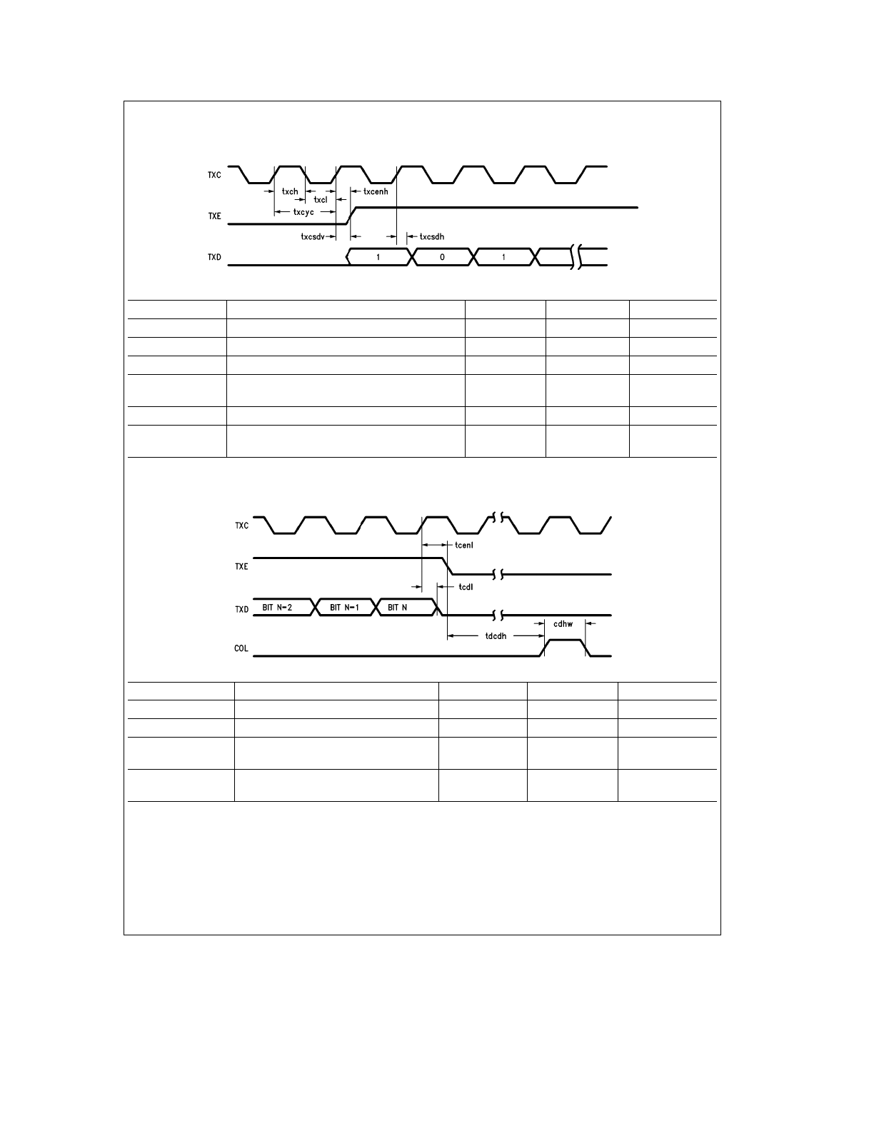
15.0 Switching Characteristics
(Continued)
Serial TimingÐTransmit (Beginning of Frame)
TL/F/8582 – 90
Symbol
Parameter
Min
Max
Units
txch
Transmit Clock High Time
36
ns
txcl
Transmit Clock Low Time
36
ns
txcyc
Transmit Clock Cycle Time
80
120
ns
txcenh
Transmit Clock to Transmit Enable High
48
ns
(Note 1)
txcsdv
Transmit Clock to Serial Data Valid
67
ns
txcsdh
Serial Data Hold Time from
10
ns
Transmit Clock High
Note 1:
The NIC issues TXEN coincident with the first bit of preamble. The first bit of preamble is always a 1.
Serial TimingÐTransmit (End of Frame, CD Heartbeat)
TL/F/8582 – 91
Symbol
Parameter
Min
Max
Units
tcdl
Transmit Clock to Data Low
55
ns
tcenl
Transmit Clock to TXEN Low
55
ns
tdcdh
TXEN Low to Start of Collision
0
64
txcyc
Detect Heartbeat (Note 1)
cycles
cdhw
Collision Detect Width
2
txcyc
cycles
Note 1:
If COL is not seen during the first 64 TX clock cycles following de-assertion of TXEN, the CDH bit in the TSR is set.
53
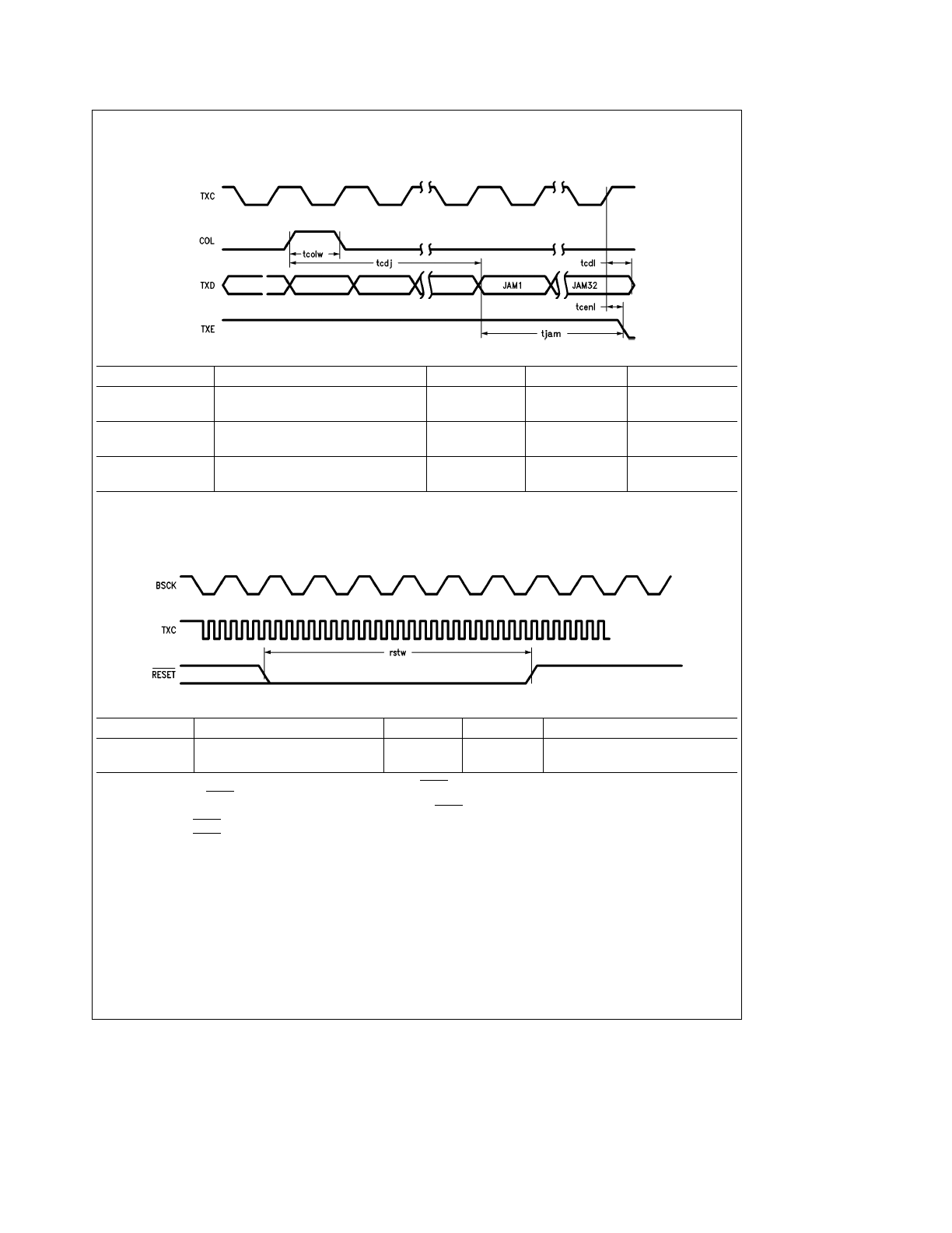
15.0 Switching Characteristics
(Continued)
Serial TimingÐTransmit (Collision)
TL/F/8582 – 92
Symbol
Parameter
Min
Max
Units
tcolw
Collision Detect Width
2
txcyc
cycles
tcdj
Delay from Collision to First
8
txcyc
Bit of Jam (Note 1)
cycles
tjam
Jam Period (Note 2)
32
txcyc
cycles
Note 1:
The NIC must synchronize to collision detect. If the NIC is in the middle of serializing a byte of data the remainder of the byte will be serialized. Thus the jam
pattern will start anywhere from 1 to 8 TXC cycles after COL is asserted.
Note 2:
The NIC always issues 32 bits of jam. The jam is all 1’s data.
Reset Timing
TL/F/8582 – 93
Symbol
Parameter
Min
Max
Units
rstw
Reset Pulse Width (Note 1)
8
BSCK Cycles or TXC Cycles
(Note 2)
Note 1:
The RESET pulse requires that BSCK and TXC be stable. On power up, RESET should not be raised until BSCK and TXC have become stable. Several
registers are affected by RESET. Consult the register descriptions for details.
Note 2:
The slower of BSCK or TXC clocks will determine the minimum time for the RESET signal to be low.
If BSCK
k
TXC then RESET e 8
c
BSCK
If TXC
k
BSCK then RESET e 8
c
TXC
54
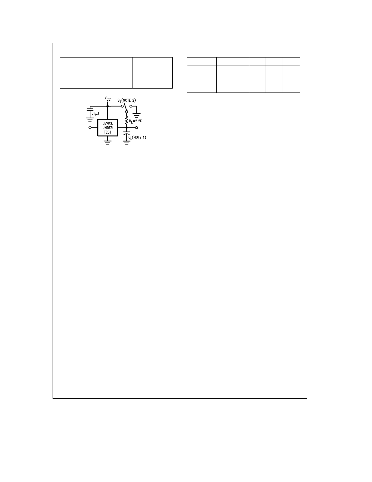
AC Timing Test Conditions
Input Pulse Levels
GND to 3.0V
Input Rise and Fall Times
5 ns
Input and Output Reference Levels
1.3V
TRI-STATE Reference Levels
Float (DV)
g
0.5V
Output Load (See Figure below)
TL/F/8582 – 94
Note 1:
C
L
e
50 pF, includes scope and jig capacitance.
Note 2:
S1 e Open for timing tests for push pull outputs.
S1 e V
CC
for V
OL
test.
S1 e GND for V
OH
test.
S1 e V
CC
for High Impedance to active low and active low to High
Impedance measurements.
S1 e GND for High Impedance to active high and active high to
High Impedance measurements.
Pin Capacitance
T
A
e
25
§
C, f
e
1 MHz
Parameter
Description
Typ
Max
Unit
C
IN
Input
7
15
pF
Capacitance
C
OUT
Output
7
15
pF
Capacitance
Note:
This parameter is sampled and not 100% tested.
DERATING FACTOR
Output timings are measured with a purely capacitave load
for 50 pF. The following correction factor can be used for
other loads:
C
L
t
50 pf:
a
0.3 ns/pF (for all outputs except TXE, TXD,
and LBK)
55
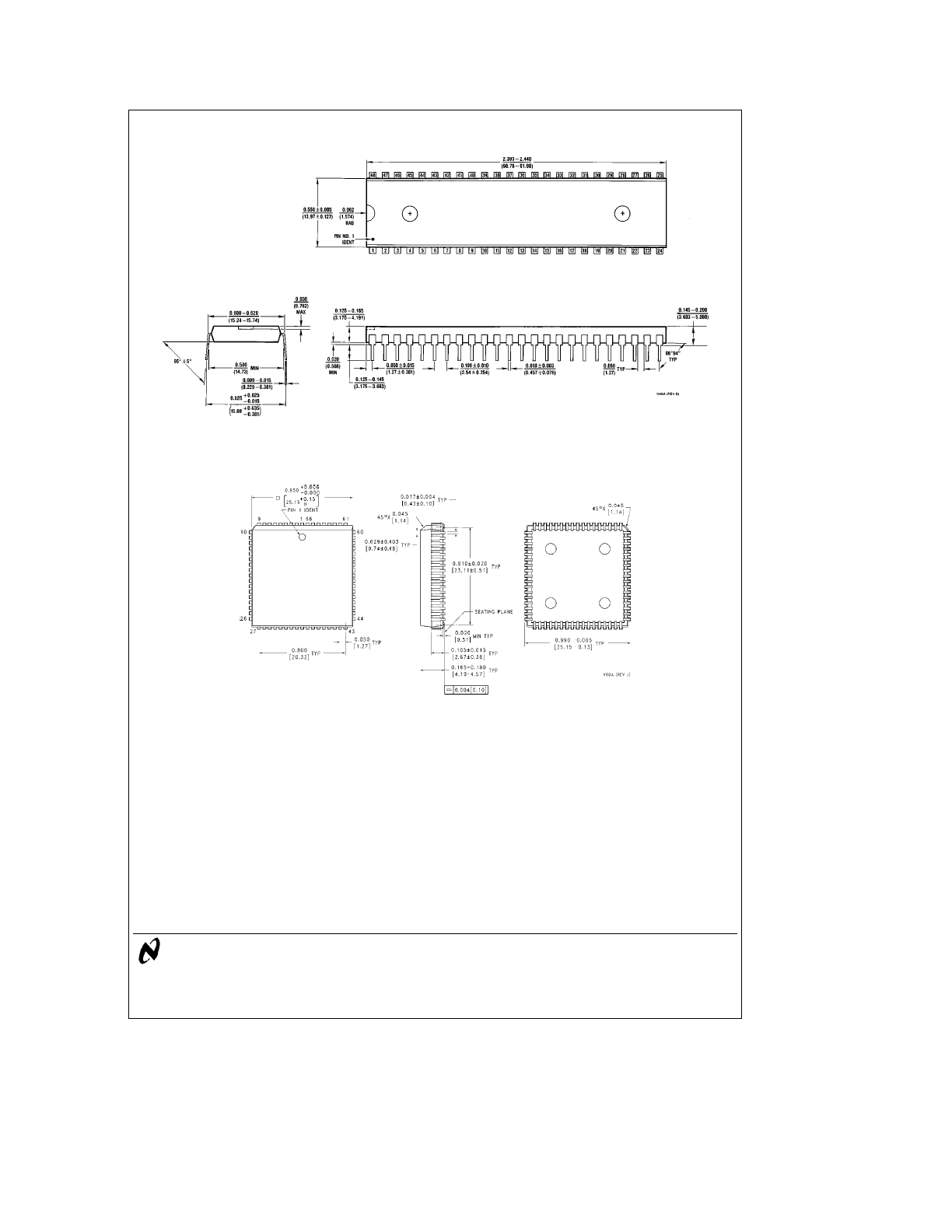
DP8390D/NS32490D
NIC
Network
Interface
Controller
16.0 Physical Dimensions
inches (millimeters)
Lit.
Ý
103052
Molded Dual-In-Line Package (N)
Order Number DP8390DN
NS Package Number N48A
Plastic Chip Carrier (V)
Order Number DP8390DV
NS Package Number V68A
LIFE SUPPORT POLICY
NATIONAL’S PRODUCTS ARE NOT AUTHORIZED FOR USE AS CRITICAL COMPONENTS IN LIFE SUPPORT
DEVICES OR SYSTEMS WITHOUT THE EXPRESS WRITTEN APPROVAL OF THE PRESIDENT OF NATIONAL
SEMICONDUCTOR CORPORATION. As used herein:
1. Life support devices or systems are devices or
2. A critical component is any component of a life
systems which, (a) are intended for surgical implant
support device or system whose failure to perform can
into the body, or (b) support or sustain life, and whose
be reasonably expected to cause the failure of the life
failure to perform, when properly used in accordance
support device or system, or to affect its safety or
with instructions for use provided in the labeling, can
effectiveness.
be reasonably expected to result in a significant injury
to the user.
National Semiconductor
National Semiconductor
National Semiconductor
National Semiconductor
Corporation
Europe
Hong Kong Ltd.
Japan Ltd.
1111 West Bardin Road
Fax: (
a
49) 0-180-530 85 86
13th Floor, Straight Block,
Tel: 81-043-299-2309
Arlington, TX 76017
Email: cnjwge
@
tevm2.nsc.com
Ocean Centre, 5 Canton Rd.
Fax: 81-043-299-2408
Tel: 1(800) 272-9959
Deutsch Tel: (
a
49) 0-180-530 85 85
Tsimshatsui, Kowloon
Fax: 1(800) 737-7018
English
Tel: (
a
49) 0-180-532 78 32
Hong Kong
Fran
3ais Tel: (
a
49) 0-180-532 93 58
Tel: (852) 2737-1600
Italiano
Tel: (
a
49) 0-180-534 16 80
Fax: (852) 2736-9960
National does not assume any responsibility for use of any circuitry described, no circuit patent licenses are implied and National reserves the right at any time without notice to change said circuitry and specifications.