

2007 - 2016 Microchip Technology Inc.
DS000002251A-page 1
Highlights
• Integrated USB 2.0 Compatible 7-Port Hub
- 7 Transaction Translators for highest perfor-
mance
- High-Speed (480Mbits/s), Full-Speed
(12Mbits/s) and Low-Speed (1.5Mbits/s)
compatible
- Full power management with per port or
ganged, selectable power control
- Detects Bus-Power/Self-Power source and
changes mode automatically
• Complete USB Specification 2.0 Compatibility
- Includes USB 2.0 Transceivers
• VID/PID/DID, and Port Configuration for Hub via:
- Single Serial I
2
C EEPROM
- SMBus Slave Port
• Default VID/PID/DID, allows functionality when
configuration EEPROM is absent
• Hardware Strapping options allow for configura-
tion without an external EEPROM or SMBus Host
• On-Board 24MHz Crystal Driver Circuit or 24 MHz
external clock driver
• Internal PLL for 480MHz USB 2.0 Sampling
• Internal 1.8V Linear Voltage Regulator
• Integrated USB termination and Pull-up/Pull-down
resistors
• Internal Short Circuit protection of USB differential
signal pins
• 1.8 Volt Low Power Core Operation
• 3.3 Volt I/O with 5V Input Tolerance
• 80-Pin TQFP RoHS compliant package
USB2507
Integrated USB 2.0 Compatible 7-Port Hub

USB2507
DS000002251A-page 2
2007 - 2016 Microchip Technology Inc.
TO OUR VALUED CUSTOMERS
It is our intention to provide our valued customers with the best documentation possible to ensure successful use of your Microchip
products. To this end, we will continue to improve our publications to better suit your needs. Our publications will be refined and
enhanced as new volumes and updates are introduced.
If you have any questions or comments regarding this publication, please contact the Marketing Communications Department via
E-mail at
docerrors@microchip.com
. We welcome your feedback.
Most Current Data Sheet
To obtain the most up-to-date version of this data sheet, please register at our Worldwide Web site at:
http://www.microchip.com
You can determine the version of a data sheet by examining its literature number found on the bottom outside corner of any page.
The last character of the literature number is the version number, (e.g., DS30000000A is version A of document DS30000000).
Errata
An errata sheet, describing minor operational differences from the data sheet and recommended workarounds, may exist for cur-
rent devices. As device/documentation issues become known to us, we will publish an errata sheet. The errata will specify the
revision of silicon and revision of document to which it applies.
To determine if an errata sheet exists for a particular device, please check with one of the following:
• Microchip’s Worldwide Web site;
http://www.microchip.com
• Your local Microchip sales office (see last page)
When contacting a sales office, please specify which device, revision of silicon and data sheet (include -literature number) you are
using.
Customer Notification System
Register on our web site at
www.microchip.com
to receive the most current information on all of our products.

2007 - 2016 Microchip Technology Inc.
DS000002251A-page 3
USB2507
Table of Contents
1.0 Introduction ..................................................................................................................................................................................... 4
2.0 Pin Table 7-Port .............................................................................................................................................................................. 5
3.0 Pin Configuration 7-Port Hub .......................................................................................................................................................... 6
4.0 7-Port Hub Block Diagram .............................................................................................................................................................. 7
5.0 Functional Block Description ......................................................................................................................................................... 12
6.0 XNOR Test .................................................................................................................................................................................... 30
7.0 DC Parameters ............................................................................................................................................................................. 31
8.0 AC Specifications .......................................................................................................................................................................... 35
9.0 Package Outline ............................................................................................................................................................................ 36
Appendix A: Data Sheet Revision History ........................................................................................................................................... 37
The Microchip Web Site ...................................................................................................................................................................... 38
Customer Change Notification Service ............................................................................................................................................... 38
Customer Support ............................................................................................................................................................................... 38
Product Identification System ............................................................................................................................................................. 40

USB2507
DS000002251A-page 4
2007 - 2016 Microchip Technology Inc.
1.0
INTRODUCTION
The Microchip 7-Port Hub is fully compliant with the USB 2.0 Specification and will attach to a USB host as a Full-Speed
Hub or as a Full-/High-Speed Hub. The 7-Port Hub supports Low-Speed, Full-Speed, and High-Speed (if operating as
a High-Speed Hub) downstream devices on all of the enabled downstream ports.
A dedicated Transaction Translator (TT) is available for each downstream facing port. This architecture ensures maxi-
mum USB throughput for each connected device when operating with mixed-speed peripherals.
The Hub works with an external USB power distribution switch device to control V
BUS
switching to downstream ports,
and to limit current and sense over-current conditions.
All required resistors on the USB ports are integrated into the Hub. This includes all series termination resistors on D+
and D– pins and all required pull-down and pull-up resistors on D+ and D– pins. The over-current sense inputs for the
downstream facing ports have internal pull-up resistors.
Throughout this document the upstream facing port of the hub will be referred to as the upstream port, and the down-
stream facing ports will be called the downstream ports.
1.1
OEM Selectable Features
A default configuration is available in the USB2507 following a reset. This configuration may be sufficient for some appli-
cations. Strapping option pins make it possible to modify a limited sub-set of the configuration options.
The USB2507 may also be configured by an external EEPROM or a microcontroller. When using the microcontroller
interface, the Hub appears as an SMBus slave device. If the Hub is pin-strapped for external EEPROM configuration
but no external EEPROM is present, then a value of ‘0’ will be written to all configuration data bit fields (the hub will
attach to the host with all ‘0’ values).
The 7-Port Hub supports several OEM selectable features:
• Operation as a Self-Powered USB Hub or as a Bus-Powered USB Hub.
• Operation as a Dynamic-Powered Hub (Hub operates as a Bus-Powered device if a local power source is not
available and switches to Self-Powered operation when a local power source is available).
• Optional OEM configuration via I
2
C EEPROM or via the industry standard SMBus interface from an external
SMBus Host.
• LED indicator support.
• Compound device support (port is permanently hardwired to a downstream USB peripheral device).
• Hardware strapping options enable configuration of the following features.
- Non-Removable Ports
- Port Power Polarity (active high or active low logic)
- Port Disable
- LED support
- MTT enable
- Ganged Vs Port power switching and over-current sensing

2007 - 2016 Microchip Technology Inc.
DS000002251A-page 5
USB2507
2.0
PIN TABLE 7-PORT
TABLE 2-1:
7-PORT PIN TABLE
UPSTREAM USB 2.0 INTERFACE (3 PINS)
USBDP0
USBDN0
VBUS_DET
7-PORT USB 2.0 INTERFACE (44 PINS)
USBDP1
USBDN1
USBDP2
USBDN2
USBDP3
USBDN3
USBDP4
USBDN4
USBDP5
USBDN5
USBDP6
USBDN6
USBDP7
USBDN7
GR1/
NON_REM0
GR2/
NON_REM1
GR3/
PRT_DIS0
GR4/
PRT_DIS1
GR5
GR6
GR7
AM1/
GANG_EN
AM2/
MTT_EN
AM3
AM4/
LED_EN
AM5
AM6
AM7
PRTPWR1
PRTPWR2
PRTPWR3
PRTPWR4
PRTPWR5
PRTPWR6
PRTPWR7
OCS1_N
OCS2_N
OCS3_N
OCS4_N
OCS5_N
OCS6_N
OCS7_N
PRTPWR_POL
RBIAS
SERIAL PORT INTERFACE (3 PINS)
SDA/SMBDATA
SCL/SMBCLK/
CFG_SEL0
CFG_SEL1
MISC (8 PINS)
XTAL1/CLKIN
XTAL2
RESET_N
SELF_PWR
ATEST/
REG_EN
CLKIN_EN
TEST1
TEST0
POWER, GROUND (22 PINS)
USB2507
DS000002251A-page 6
2007 - 2016 Microchip Technology Inc.
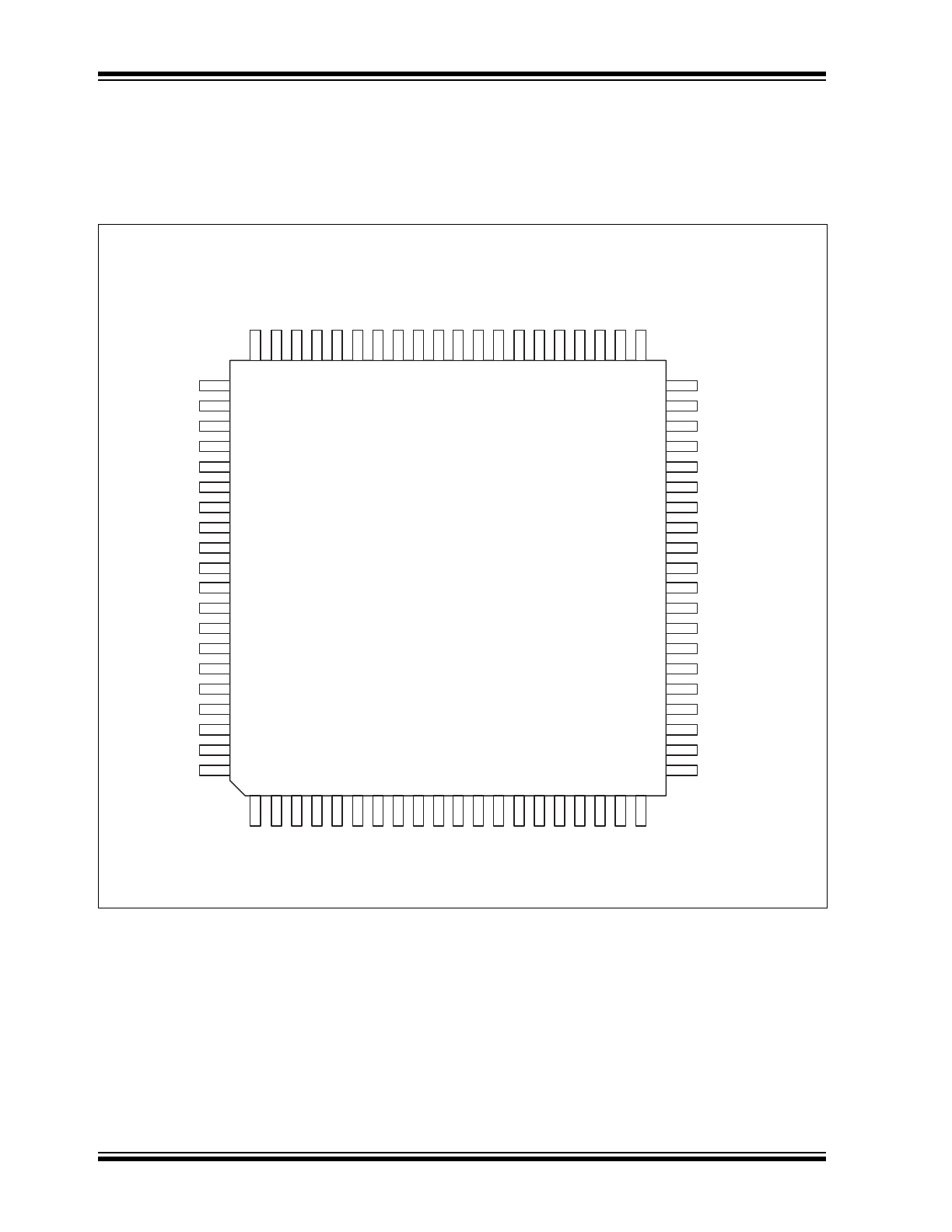
3.0
PIN CONFIGURATION 7-PORT HUB
FIGURE 3-1:
7-PORT 80-PIN TQFP
USBDP0
VDDA33
USBDN0
VSS
USBDN1
USBDP1
VDDA33
USBDP2
USBDN2
GR7
PRTPWR1
AM7
GR6
GR5
AM6
AM5
VDD18
VSS
USB2507
61
80
40
21
20
60
41
VSS
VSS
VDD18
VDD33
GR4/PRT_DIS1
AM4/LED_EN
VSS
1
XTAL2
XTAL1/CLKIN
VDDA18PLL
GR3/PRT_DIS0
AM3
GR2/NON_REM1
AM2/MTT_EN
VDDA33PLL
ATEST/REG_EN
RBIAS
VSS
GR1/NON_REM0
AM1/GANG_EN
SDA/SMBDATA
SCL/SMBCLK/CFG_SEL0
TEST0
PR
TPWR_POL
RESET_N
VBUS_DET
PR
TPWR7
OCS7_N
CLKIN_EN
OCS5_N
PR
TPWR6
OCS6_N
VSS
VDD18
VDD33CR
PR
TPWR4
OCS4_N
PR
TPWR5
OCS2_N
PR
TPWR3
OCS3_N
OCS1_N
PR
TPWR2
TEST1
SELF_PWR
CFG_SEL1
VDDA33
USBDP7
USBDN7
VSS
USBDN5
VSS
USBDN6
USBDP6
USBDN4
USBDP4
VDDA33
USBDP5
VDDA33
USBDP3
USBDN3
VSS
2007 - 2016 Microchip Technology Inc.
DS000002251A-page 7
USB2507
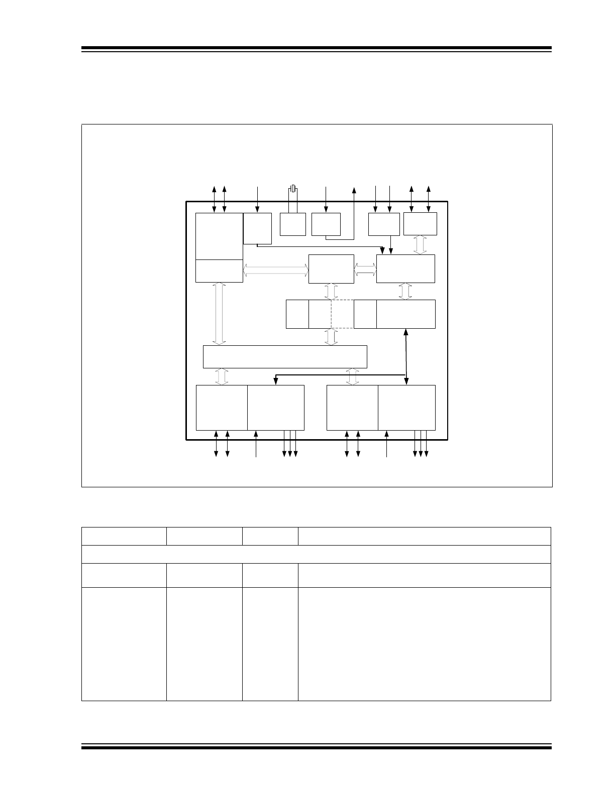
4.0
7-PORT HUB BLOCK DIAGRAM
FIGURE 4-1:
7-PORT BLOCK DIAGRAM
TABLE 4-1:
7-PORT HUB PIN DESCRIPTIONS
Name
Symbol
Type
Function
UPSTREAM USB 2.0 INTERFACE
USB Bus Data
USBDN0
USBDP0
IO-U
These pins connect to the upstream USB bus data signals.
Detect Upstream
VBUS Power
VBUS_DET
I/O12
Detects state of Upstream VBUS power. The Microchip Hub
monitors VBUS_DET to determine when to assert the internal
D+ pull-up resistor (signaling a connect event).
When designing a detachable hub, this pin must be
connected to the VBUS power pin of the USB port that is
upstream of the hub. (Use of a weak pull-down resistor is
recommended.)
For self-powered applications with a permanently attached
host, this pin must be pulled-up to either 3.3V or 5.0V
(typically VDD33).
Upstream
V
BUS
Upstream
PHY
Upstream
USB Data
Repeater
Controller
SIE
Serial
Interface
PLL
24 MHz
Crystal
To
EEPROM
or SMBus
Master
Routing Logic
SCL
SD
TT
#1
TT
#2
...
TT
#7
Port
Controller
Downstream
PHY #1
Port #1
OC Sense
Switch Driver
LED Drivers
Downstream
PHY #7
Port #7
OC Sense
Switch Driver
LED Drivers
...
Downstream
USB Data
OC
Sense
Switch/LED
Drivers
Downstream
USB Data
OC
Sense
Switch/LED
Drivers
V
BUS
Power
Detect
Pin
Strapping
Options
Internal
Defaults
Select
3.3V
1.8V
Reg.
1.8V
Cap

USB2507
DS000002251A-page 8
2007 - 2016 Microchip Technology Inc.
7-PORT USB 2.0 HUB INTERFACE
High-Speed USB
Data
USBDN[7:1]
USBDP[7:1]
IO-U
These pins connect to the downstream USB peripheral
devices attached to the Hub’s ports.
USB Power Enable
PRTPWR[7:1]
O12
Enables power to USB peripheral devices (downstream).
The active signal level of the PRTPWR7:1 pins is determined
by the Power Polarity Strapping function of the
PRTPWR_POL pin.
Ports [7:5] Green
LED
GR[7:5]
I/O12
Green indicator LED’s for ports[7:5]. LED is active low
Port 4:3 Green
LED
&
Port Disable
strapping option.
GR[4:3]/
PRT_DIS[1:0]
I/O12
Green indicator LED for ports 4 and 3. Will be active low
when LED support is enabled via EEPROM or SMBus.
If the hub is configured by the internal default configuration,
these pins will be sampled at RESET_N negation to
determine if ports [7:5] will be permanently disabled. Also, the
active state of the LED’s will be determined as follows:
PRT_DIS[1:0] = ‘00’, All ports are enabled,
GR4 is active high,
GR3 is active high.
PRT_DIS[1:0] = ‘01’, Port 7 is disabled,
GR4 is active high,
GR3 is active low.
PRT_DIS[1:0] = ‘10’, Ports 7 & 6 are disabled,
GR4 is active low,
GR3 is active high.
PRT_DIS[1:0] = ‘11’, Ports 7, 6 & 5 are disabled,
GR4 is active low,
GR3 is active low.
Port [2:1] Green
LED
&
Port Non-
Removable
strapping option.
GR[2:1]/
NON_REM[1:0]
I/O12
Green indicator LED for ports 2 and 1. Will be active low
when LED support is enabled via EEPROM or SMBus.
If the hub is configured by the internal default configuration,
these pins will be sampled at RESET_N negation to
determine if ports [3:1] contain permanently attached (non-
removable) devices. Also, the active state of the LED’s will be
determined as follows:
NON_REM[1:0] = ‘00’, All ports are removable,
GR2 is active high,
GR1 is active high.
NON_REM[1:0] = ‘01’, Port 1 is non-removable,
GR2 is active high,
GR1 is active low.
NON_REM[1:0] = ‘10’, Ports 1 & 2 are non-removable,
GR2 is active low,
GR1 is active high.
NON_REM[1:0] = ‘11’, Ports 1, 2, & 3 are non-removable,
GR2 is active low,
GR1 is active low.
Ports [7:5] Amber
LED
AM[7:5]
I/O12
Amber indicator LED’s for ports [7:5], LED is active low.
TABLE 4-1:
7-PORT HUB PIN DESCRIPTIONS (CONTINUED)
Name
Symbol
Type
Function

2007 - 2016 Microchip Technology Inc.
DS000002251A-page 9
USB2507
Port 4 Amber LED
&
LED Enable
strapping option
AM4/
LED_EN
I/O12
Amber indicator LED for port 4. Will be active low when LED
support is enabled via EEPROM or SMBus.
If the hub is configured by the internal default configuration,
this pin will be sampled at RESET_N negation to determine
if LED support is enabled or disabled. Also, the active state
of the LED will be determined as follows:
‘0’ = LED support is disabled, LED is inactive
‘1’ = LED Support is enabled, LED is active low.
Port 3 Amber LED
AM3
I/O12
Amber indicator LED for port 3. Signal will be active low.
Port 2 Amber LED
&
MTT Disable
AM2/
MTT_EN
I/O12
Amber indicator LED for port 2. Will be active low when LED
support is enabled via EEPROM or SMBus.
If the hub is configured by the internal default configuration,
this pin will be sampled at RESET_N negation to determine
if MTT support is disabled (STT only). Also, the active state
of the LED will be determined as follows:
‘0’ = MTT support is disabled, LED is active high
‘1’ = MTT support is enabled, LED is active low.
Port 1 Amber LED
&
Gang Power
Switching and
Current Sensing
strapping option.
AM1/
GANG_EN
I/O12
Amber indicator LED for port 1, Will be active low when LED
support is enabled via EEPROM or SMBus.
If the hub is configured by the internal default configuration,
this pin will be sampled at RESET_N negation to determine
if downstream port power switching and current sensing are
ganged, or individual port-by-port. Also, the active state of the
LED will be determined as follows:
‘0’ = Port-by-port sensing & switching, LED is active high
‘1’ = Ganged sensing & switching, LED is active low.
Port Power Polarity
strapping.
PRTPWR_POL
I/O12
Port Power Polarity strapping determination for the active
signal polarity of the 7:1PRTPWR pins.
While RESET_N is asserted, the logic state of this pin will
(though the use of internal combinatorial logic) determine the
active state of the 7:1PRTPWR pins in order to ensure that
downstream port power is not inadvertently enabled to
inactive ports during a hardware reset.
On the rising edge of RESET_N (see the applicable
RESET_N timing table in
Section 5.6.1
), the logic value will
be latched internally, and will retain the active signal polarity
for the PRTPWR7:1 pin.
‘1’ = PRTPWR7:1 pins have an active ‘high’ polarity
‘0’ = PRTPWR7:1 pins have an active ‘low’ polarity
Over Current
Sense
OCS7:1_N
IPU
Input from external current monitor indicating an over-current
condition. {Note: Contains internal pull-up to 3.3V supply}
USB Transceiver
Bias
RBIAS
I-R
A 12.0k
(resistor is attached from ground to this pin
to set the transceiver’s internal bias settings.
TABLE 4-1:
7-PORT HUB PIN DESCRIPTIONS (CONTINUED)
Name
Symbol
Type
Function
USB2507
DS000002251A-page 10
2007 - 2016 Microchip Technology Inc.
SERIAL PORT INTERFACE
Serial Data/SMB
Data
SDA/SMBDATA
IOSD12
(Serial Data)/(SMB Data) signal.
Serial Clock/SMB
Clock
&
Config Select 0
SCL/SMBCLK/
CFG_SEL0
IOSD12
(Serial Clock)/(SMB Clock) signal. This multifunction pin is
read on the rising edge of RESET_N (see the applicable
RESET_N timing table in
Section 5.6.1
) and will determine
the hub configuration method as described in
Table 4-2
.
Configuration
Programming
Select
CFG_SEL1
I
This multifunction pin is read on the rising edge of RESET_N
(see the applicable RESET_N timing table in
Section 5.6.1
)
and will determine the hub configuration method as described
in
Table 4-2
.
TABLE 4-2:
SMBUS OR EEPROM INTERFACE BEHAVIOR
CFG_SEL1
CFG_SEL0
SMBus or EEPROM Interface Behavior
0
0
Reserved
0
1
Configured as an SMBus slave for external download of user-
defined descriptors. SMBus slave address is 0101100
1
0
Internal Default Configuration via strapping options.
1
1
2-wire (I
2
C) EEPROMS are supported,
TABLE 4-3:
MISCELLANEOUS PINS
Name
Symbol
Type
Function
Crystal
Input/External
Clock Input
XTAL1/
CLKIN
ICLKx
24MHz crystal or external clock input.
This pin connects to either one terminal of the crystal or to
an external 24MHz clock when a crystal is not used.
Crystal Output
XTAL2
OCLKx
24MHz Crystal
This is the other terminal of the crystal, or left unconnected
when an external clock source is used to drive
XTAL1/CLKIN. It must not be used to drive any external
circuitry other than the crystal circuit.
Clock Input
Enable
CLKIN_EN
I
Clock In Enable:
Low = XTAL1 and XTAL2 pins configured for use with
external crystal
High = XTAL1 pin configured as CLKIN, and must be
driven by an external CMOS clock.
RESET Input
RESET_N
IS
This active low signal is used by the system to reset the
chip. The minimum active low pulse is 1us.
Self-Power /
Bus-Power
Detect
SELF_PWR
I
Detects availability of local self-power source.
Low = Self/local power source is NOT available (i.e., Hub
gets all power from Upstream USB VBus).
High = Self/local power source is available.
TEST Pins
TEST[1:0]
IPD
Used for testing the chip. User must treat as a no-connect
or connect to ground.
Analog Test
&
Internal 1.8V
voltage regulator
enable
ATEST/
REG_EN
AIO
This signal is used for testing the analog section of the
chip, and to enable or disable the internal 1.8v regulator.
This pin must be connected to VDDA33 to enable the
internal 1.8V regulator, or to VSS to disable the internal
regulator.
When the internal regulator is enabled, the 1.8V power
pins must be left unconnected, except for the required
bypass capacitors.When the PHY is in test mode, the
internal regulator is disabled and the ATEST pin functions
as a test pin.
TABLE 4-1:
7-PORT HUB PIN DESCRIPTIONS (CONTINUED)
Name
Symbol
Type
Function
2007 - 2016 Microchip Technology Inc.
DS000002251A-page 1
Highlights
• Integrated USB 2.0 Compatible 7-Port Hub
- 7 Transaction Translators for highest perfor-
mance
- High-Speed (480Mbits/s), Full-Speed
(12Mbits/s) and Low-Speed (1.5Mbits/s)
compatible
- Full power management with per port or
ganged, selectable power control
- Detects Bus-Power/Self-Power source and
changes mode automatically
• Complete USB Specification 2.0 Compatibility
- Includes USB 2.0 Transceivers
• VID/PID/DID, and Port Configuration for Hub via:
- Single Serial I
2
C EEPROM
- SMBus Slave Port
• Default VID/PID/DID, allows functionality when
configuration EEPROM is absent
• Hardware Strapping options allow for configura-
tion without an external EEPROM or SMBus Host
• On-Board 24MHz Crystal Driver Circuit or 24 MHz
external clock driver
• Internal PLL for 480MHz USB 2.0 Sampling
• Internal 1.8V Linear Voltage Regulator
• Integrated USB termination and Pull-up/Pull-down
resistors
• Internal Short Circuit protection of USB differential
signal pins
• 1.8 Volt Low Power Core Operation
• 3.3 Volt I/O with 5V Input Tolerance
• 80-Pin TQFP RoHS compliant package
USB2507
Integrated USB 2.0 Compatible 7-Port Hub
USB2507
DS000002251A-page 2
2007 - 2016 Microchip Technology Inc.
TO OUR VALUED CUSTOMERS
It is our intention to provide our valued customers with the best documentation possible to ensure successful use of your Microchip
products. To this end, we will continue to improve our publications to better suit your needs. Our publications will be refined and
enhanced as new volumes and updates are introduced.
If you have any questions or comments regarding this publication, please contact the Marketing Communications Department via
E-mail at
docerrors@microchip.com
. We welcome your feedback.
Most Current Data Sheet
To obtain the most up-to-date version of this data sheet, please register at our Worldwide Web site at:
http://www.microchip.com
You can determine the version of a data sheet by examining its literature number found on the bottom outside corner of any page.
The last character of the literature number is the version number, (e.g., DS30000000A is version A of document DS30000000).
Errata
An errata sheet, describing minor operational differences from the data sheet and recommended workarounds, may exist for cur-
rent devices. As device/documentation issues become known to us, we will publish an errata sheet. The errata will specify the
revision of silicon and revision of document to which it applies.
To determine if an errata sheet exists for a particular device, please check with one of the following:
• Microchip’s Worldwide Web site;
http://www.microchip.com
• Your local Microchip sales office (see last page)
When contacting a sales office, please specify which device, revision of silicon and data sheet (include -literature number) you are
using.
Customer Notification System
Register on our web site at
www.microchip.com
to receive the most current information on all of our products.
2007 - 2016 Microchip Technology Inc.
DS000002251A-page 3
USB2507
Table of Contents
1.0 Introduction ..................................................................................................................................................................................... 4
2.0 Pin Table 7-Port .............................................................................................................................................................................. 5
3.0 Pin Configuration 7-Port Hub .......................................................................................................................................................... 6
4.0 7-Port Hub Block Diagram .............................................................................................................................................................. 7
5.0 Functional Block Description ......................................................................................................................................................... 12
6.0 XNOR Test .................................................................................................................................................................................... 30
7.0 DC Parameters ............................................................................................................................................................................. 31
8.0 AC Specifications .......................................................................................................................................................................... 35
9.0 Package Outline ............................................................................................................................................................................ 36
Appendix A: Data Sheet Revision History ........................................................................................................................................... 37
The Microchip Web Site ...................................................................................................................................................................... 38
Customer Change Notification Service ............................................................................................................................................... 38
Customer Support ............................................................................................................................................................................... 38
Product Identification System ............................................................................................................................................................. 40
USB2507
DS000002251A-page 4
2007 - 2016 Microchip Technology Inc.
1.0
INTRODUCTION
The Microchip 7-Port Hub is fully compliant with the USB 2.0 Specification and will attach to a USB host as a Full-Speed
Hub or as a Full-/High-Speed Hub. The 7-Port Hub supports Low-Speed, Full-Speed, and High-Speed (if operating as
a High-Speed Hub) downstream devices on all of the enabled downstream ports.
A dedicated Transaction Translator (TT) is available for each downstream facing port. This architecture ensures maxi-
mum USB throughput for each connected device when operating with mixed-speed peripherals.
The Hub works with an external USB power distribution switch device to control V
BUS
switching to downstream ports,
and to limit current and sense over-current conditions.
All required resistors on the USB ports are integrated into the Hub. This includes all series termination resistors on D+
and D– pins and all required pull-down and pull-up resistors on D+ and D– pins. The over-current sense inputs for the
downstream facing ports have internal pull-up resistors.
Throughout this document the upstream facing port of the hub will be referred to as the upstream port, and the down-
stream facing ports will be called the downstream ports.
1.1
OEM Selectable Features
A default configuration is available in the USB2507 following a reset. This configuration may be sufficient for some appli-
cations. Strapping option pins make it possible to modify a limited sub-set of the configuration options.
The USB2507 may also be configured by an external EEPROM or a microcontroller. When using the microcontroller
interface, the Hub appears as an SMBus slave device. If the Hub is pin-strapped for external EEPROM configuration
but no external EEPROM is present, then a value of ‘0’ will be written to all configuration data bit fields (the hub will
attach to the host with all ‘0’ values).
The 7-Port Hub supports several OEM selectable features:
• Operation as a Self-Powered USB Hub or as a Bus-Powered USB Hub.
• Operation as a Dynamic-Powered Hub (Hub operates as a Bus-Powered device if a local power source is not
available and switches to Self-Powered operation when a local power source is available).
• Optional OEM configuration via I
2
C EEPROM or via the industry standard SMBus interface from an external
SMBus Host.
• LED indicator support.
• Compound device support (port is permanently hardwired to a downstream USB peripheral device).
• Hardware strapping options enable configuration of the following features.
- Non-Removable Ports
- Port Power Polarity (active high or active low logic)
- Port Disable
- LED support
- MTT enable
- Ganged Vs Port power switching and over-current sensing
2007 - 2016 Microchip Technology Inc.
DS000002251A-page 5
USB2507
2.0
PIN TABLE 7-PORT
TABLE 2-1:
7-PORT PIN TABLE
UPSTREAM USB 2.0 INTERFACE (3 PINS)
USBDP0
USBDN0
VBUS_DET
7-PORT USB 2.0 INTERFACE (44 PINS)
USBDP1
USBDN1
USBDP2
USBDN2
USBDP3
USBDN3
USBDP4
USBDN4
USBDP5
USBDN5
USBDP6
USBDN6
USBDP7
USBDN7
GR1/
NON_REM0
GR2/
NON_REM1
GR3/
PRT_DIS0
GR4/
PRT_DIS1
GR5
GR6
GR7
AM1/
GANG_EN
AM2/
MTT_EN
AM3
AM4/
LED_EN
AM5
AM6
AM7
PRTPWR1
PRTPWR2
PRTPWR3
PRTPWR4
PRTPWR5
PRTPWR6
PRTPWR7
OCS1_N
OCS2_N
OCS3_N
OCS4_N
OCS5_N
OCS6_N
OCS7_N
PRTPWR_POL
RBIAS
SERIAL PORT INTERFACE (3 PINS)
SDA/SMBDATA
SCL/SMBCLK/
CFG_SEL0
CFG_SEL1
MISC (8 PINS)
XTAL1/CLKIN
XTAL2
RESET_N
SELF_PWR
ATEST/
REG_EN
CLKIN_EN
TEST1
TEST0
POWER, GROUND (22 PINS)
USB2507
DS000002251A-page 6
2007 - 2016 Microchip Technology Inc.
3.0
PIN CONFIGURATION 7-PORT HUB
FIGURE 3-1:
7-PORT 80-PIN TQFP
USBDP0
VDDA33
USBDN0
VSS
USBDN1
USBDP1
VDDA33
USBDP2
USBDN2
GR7
PRTPWR1
AM7
GR6
GR5
AM6
AM5
VDD18
VSS
USB2507
61
80
40
21
20
60
41
VSS
VSS
VDD18
VDD33
GR4/PRT_DIS1
AM4/LED_EN
VSS
1
XTAL2
XTAL1/CLKIN
VDDA18PLL
GR3/PRT_DIS0
AM3
GR2/NON_REM1
AM2/MTT_EN
VDDA33PLL
ATEST/REG_EN
RBIAS
VSS
GR1/NON_REM0
AM1/GANG_EN
SDA/SMBDATA
SCL/SMBCLK/CFG_SEL0
TEST0
PR
TPWR_POL
RESET_N
VBUS_DET
PR
TPWR7
OCS7_N
CLKIN_EN
OCS5_N
PR
TPWR6
OCS6_N
VSS
VDD18
VDD33CR
PR
TPWR4
OCS4_N
PR
TPWR5
OCS2_N
PR
TPWR3
OCS3_N
OCS1_N
PR
TPWR2
TEST1
SELF_PWR
CFG_SEL1
VDDA33
USBDP7
USBDN7
VSS
USBDN5
VSS
USBDN6
USBDP6
USBDN4
USBDP4
VDDA33
USBDP5
VDDA33
USBDP3
USBDN3
VSS
2007 - 2016 Microchip Technology Inc.
DS000002251A-page 7
USB2507
4.0
7-PORT HUB BLOCK DIAGRAM
FIGURE 4-1:
7-PORT BLOCK DIAGRAM
TABLE 4-1:
7-PORT HUB PIN DESCRIPTIONS
Name
Symbol
Type
Function
UPSTREAM USB 2.0 INTERFACE
USB Bus Data
USBDN0
USBDP0
IO-U
These pins connect to the upstream USB bus data signals.
Detect Upstream
VBUS Power
VBUS_DET
I/O12
Detects state of Upstream VBUS power. The Microchip Hub
monitors VBUS_DET to determine when to assert the internal
D+ pull-up resistor (signaling a connect event).
When designing a detachable hub, this pin must be
connected to the VBUS power pin of the USB port that is
upstream of the hub. (Use of a weak pull-down resistor is
recommended.)
For self-powered applications with a permanently attached
host, this pin must be pulled-up to either 3.3V or 5.0V
(typically VDD33).
Upstream
V
BUS
Upstream
PHY
Upstream
USB Data
Repeater
Controller
SIE
Serial
Interface
PLL
24 MHz
Crystal
To
EEPROM
or SMBus
Master
Routing Logic
SCL
SD
TT
#1
TT
#2
...
TT
#7
Port
Controller
Downstream
PHY #1
Port #1
OC Sense
Switch Driver
LED Drivers
Downstream
PHY #7
Port #7
OC Sense
Switch Driver
LED Drivers
...
Downstream
USB Data
OC
Sense
Switch/LED
Drivers
Downstream
USB Data
OC
Sense
Switch/LED
Drivers
V
BUS
Power
Detect
Pin
Strapping
Options
Internal
Defaults
Select
3.3V
1.8V
Reg.
1.8V
Cap
USB2507
DS000002251A-page 8
2007 - 2016 Microchip Technology Inc.
7-PORT USB 2.0 HUB INTERFACE
High-Speed USB
Data
USBDN[7:1]
USBDP[7:1]
IO-U
These pins connect to the downstream USB peripheral
devices attached to the Hub’s ports.
USB Power Enable
PRTPWR[7:1]
O12
Enables power to USB peripheral devices (downstream).
The active signal level of the PRTPWR7:1 pins is determined
by the Power Polarity Strapping function of the
PRTPWR_POL pin.
Ports [7:5] Green
LED
GR[7:5]
I/O12
Green indicator LED’s for ports[7:5]. LED is active low
Port 4:3 Green
LED
&
Port Disable
strapping option.
GR[4:3]/
PRT_DIS[1:0]
I/O12
Green indicator LED for ports 4 and 3. Will be active low
when LED support is enabled via EEPROM or SMBus.
If the hub is configured by the internal default configuration,
these pins will be sampled at RESET_N negation to
determine if ports [7:5] will be permanently disabled. Also, the
active state of the LED’s will be determined as follows:
PRT_DIS[1:0] = ‘00’, All ports are enabled,
GR4 is active high,
GR3 is active high.
PRT_DIS[1:0] = ‘01’, Port 7 is disabled,
GR4 is active high,
GR3 is active low.
PRT_DIS[1:0] = ‘10’, Ports 7 & 6 are disabled,
GR4 is active low,
GR3 is active high.
PRT_DIS[1:0] = ‘11’, Ports 7, 6 & 5 are disabled,
GR4 is active low,
GR3 is active low.
Port [2:1] Green
LED
&
Port Non-
Removable
strapping option.
GR[2:1]/
NON_REM[1:0]
I/O12
Green indicator LED for ports 2 and 1. Will be active low
when LED support is enabled via EEPROM or SMBus.
If the hub is configured by the internal default configuration,
these pins will be sampled at RESET_N negation to
determine if ports [3:1] contain permanently attached (non-
removable) devices. Also, the active state of the LED’s will be
determined as follows:
NON_REM[1:0] = ‘00’, All ports are removable,
GR2 is active high,
GR1 is active high.
NON_REM[1:0] = ‘01’, Port 1 is non-removable,
GR2 is active high,
GR1 is active low.
NON_REM[1:0] = ‘10’, Ports 1 & 2 are non-removable,
GR2 is active low,
GR1 is active high.
NON_REM[1:0] = ‘11’, Ports 1, 2, & 3 are non-removable,
GR2 is active low,
GR1 is active low.
Ports [7:5] Amber
LED
AM[7:5]
I/O12
Amber indicator LED’s for ports [7:5], LED is active low.
TABLE 4-1:
7-PORT HUB PIN DESCRIPTIONS (CONTINUED)
Name
Symbol
Type
Function
2007 - 2016 Microchip Technology Inc.
DS000002251A-page 9
USB2507
Port 4 Amber LED
&
LED Enable
strapping option
AM4/
LED_EN
I/O12
Amber indicator LED for port 4. Will be active low when LED
support is enabled via EEPROM or SMBus.
If the hub is configured by the internal default configuration,
this pin will be sampled at RESET_N negation to determine
if LED support is enabled or disabled. Also, the active state
of the LED will be determined as follows:
‘0’ = LED support is disabled, LED is inactive
‘1’ = LED Support is enabled, LED is active low.
Port 3 Amber LED
AM3
I/O12
Amber indicator LED for port 3. Signal will be active low.
Port 2 Amber LED
&
MTT Disable
AM2/
MTT_EN
I/O12
Amber indicator LED for port 2. Will be active low when LED
support is enabled via EEPROM or SMBus.
If the hub is configured by the internal default configuration,
this pin will be sampled at RESET_N negation to determine
if MTT support is disabled (STT only). Also, the active state
of the LED will be determined as follows:
‘0’ = MTT support is disabled, LED is active high
‘1’ = MTT support is enabled, LED is active low.
Port 1 Amber LED
&
Gang Power
Switching and
Current Sensing
strapping option.
AM1/
GANG_EN
I/O12
Amber indicator LED for port 1, Will be active low when LED
support is enabled via EEPROM or SMBus.
If the hub is configured by the internal default configuration,
this pin will be sampled at RESET_N negation to determine
if downstream port power switching and current sensing are
ganged, or individual port-by-port. Also, the active state of the
LED will be determined as follows:
‘0’ = Port-by-port sensing & switching, LED is active high
‘1’ = Ganged sensing & switching, LED is active low.
Port Power Polarity
strapping.
PRTPWR_POL
I/O12
Port Power Polarity strapping determination for the active
signal polarity of the 7:1PRTPWR pins.
While RESET_N is asserted, the logic state of this pin will
(though the use of internal combinatorial logic) determine the
active state of the 7:1PRTPWR pins in order to ensure that
downstream port power is not inadvertently enabled to
inactive ports during a hardware reset.
On the rising edge of RESET_N (see the applicable
RESET_N timing table in
Section 5.6.1
), the logic value will
be latched internally, and will retain the active signal polarity
for the PRTPWR7:1 pin.
‘1’ = PRTPWR7:1 pins have an active ‘high’ polarity
‘0’ = PRTPWR7:1 pins have an active ‘low’ polarity
Over Current
Sense
OCS7:1_N
IPU
Input from external current monitor indicating an over-current
condition. {Note: Contains internal pull-up to 3.3V supply}
USB Transceiver
Bias
RBIAS
I-R
A 12.0k
(resistor is attached from ground to this pin
to set the transceiver’s internal bias settings.
TABLE 4-1:
7-PORT HUB PIN DESCRIPTIONS (CONTINUED)
Name
Symbol
Type
Function
USB2507
DS000002251A-page 10
2007 - 2016 Microchip Technology Inc.
SERIAL PORT INTERFACE
Serial Data/SMB
Data
SDA/SMBDATA
IOSD12
(Serial Data)/(SMB Data) signal.
Serial Clock/SMB
Clock
&
Config Select 0
SCL/SMBCLK/
CFG_SEL0
IOSD12
(Serial Clock)/(SMB Clock) signal. This multifunction pin is
read on the rising edge of RESET_N (see the applicable
RESET_N timing table in
Section 5.6.1
) and will determine
the hub configuration method as described in
Table 4-2
.
Configuration
Programming
Select
CFG_SEL1
I
This multifunction pin is read on the rising edge of RESET_N
(see the applicable RESET_N timing table in
Section 5.6.1
)
and will determine the hub configuration method as described
in
Table 4-2
.
TABLE 4-2:
SMBUS OR EEPROM INTERFACE BEHAVIOR
CFG_SEL1
CFG_SEL0
SMBus or EEPROM Interface Behavior
0
0
Reserved
0
1
Configured as an SMBus slave for external download of user-
defined descriptors. SMBus slave address is 0101100
1
0
Internal Default Configuration via strapping options.
1
1
2-wire (I
2
C) EEPROMS are supported,
TABLE 4-3:
MISCELLANEOUS PINS
Name
Symbol
Type
Function
Crystal
Input/External
Clock Input
XTAL1/
CLKIN
ICLKx
24MHz crystal or external clock input.
This pin connects to either one terminal of the crystal or to
an external 24MHz clock when a crystal is not used.
Crystal Output
XTAL2
OCLKx
24MHz Crystal
This is the other terminal of the crystal, or left unconnected
when an external clock source is used to drive
XTAL1/CLKIN. It must not be used to drive any external
circuitry other than the crystal circuit.
Clock Input
Enable
CLKIN_EN
I
Clock In Enable:
Low = XTAL1 and XTAL2 pins configured for use with
external crystal
High = XTAL1 pin configured as CLKIN, and must be
driven by an external CMOS clock.
RESET Input
RESET_N
IS
This active low signal is used by the system to reset the
chip. The minimum active low pulse is 1us.
Self-Power /
Bus-Power
Detect
SELF_PWR
I
Detects availability of local self-power source.
Low = Self/local power source is NOT available (i.e., Hub
gets all power from Upstream USB VBus).
High = Self/local power source is available.
TEST Pins
TEST[1:0]
IPD
Used for testing the chip. User must treat as a no-connect
or connect to ground.
Analog Test
&
Internal 1.8V
voltage regulator
enable
ATEST/
REG_EN
AIO
This signal is used for testing the analog section of the
chip, and to enable or disable the internal 1.8v regulator.
This pin must be connected to VDDA33 to enable the
internal 1.8V regulator, or to VSS to disable the internal
regulator.
When the internal regulator is enabled, the 1.8V power
pins must be left unconnected, except for the required
bypass capacitors.When the PHY is in test mode, the
internal regulator is disabled and the ATEST pin functions
as a test pin.
TABLE 4-1:
7-PORT HUB PIN DESCRIPTIONS (CONTINUED)
Name
Symbol
Type
Function