
2005-2016 Microchip Technology Inc.
DS00002252A-page 1
IrDA Controller
• IrDA v1.1 FIR and SIR Compliant Controller, with
9.6K, 19.2K, 38.4K, 57.6K, 115.2K, 0.576Mbps,
1.152Mpbs and 4Mbps data rate support.
Flash Media Controller
• Complete System Solution for interfacing Smart-
Media
™
(SM) or xD Picture Card
™
(xD)
1
, Memory
Stick
™
(MS), High Speed Memory Stick (HSMS),
Memory Stick PRO (MSPRO), MS Duo
™
, Secure
Digital (SD), High Speed SD, Mini-Secure Digital
(Mini-SD), TransFlash (SD), MultiMediaCard
™
(MMC), Reduced Size MultiMediaCard (RS-
MMC), NAND Flash, Compact Flash
™
(CF) and
CF Ultra
™
I & II, and CF form-factor ATA hard
drives to Hi-Speed USB
- Supports USB Bulk Only Mass Storage Com-
pliant Bootable BIOS
• Support for simultaneous operation of all above
devices. (only one at a time of each of the follow-
ing groups supported: CF or ATA drive, SM or XD
or NAND, SD or MMC)
• On-Chip 4-Bit High Speed Memory Stick and MS
PRO Hardware Circuitry
• On-Chip firmware reads and writes High Speed
Memory Stick and MS PRO
• 1-bit ECC correction performed in hardware for
maximum efficiency
• Hardware support for SD Security Command
Extensions
• On-chip power FETs with short circuit protection
for supplying flash media card power
• USB Bus Power Certified
• 3.3 Volt I/O with 5V input tolerance on VBUS/
GPIO3
• Complete USB Specification 2.0 Compatibility for
Bus Powered Operation
- Includes Hi-Speed USB Transceiver
- A Bi-directional Control and two Bi-directional
Bulk Endpoints are provided.
• 8051 8 bit microprocessor
- Provides low speed control functions
- 30 Mhz execution speed at 1 clock per
instruction cycle average
- 12K Bytes of internal SRAM for general pur-
pose scratchpad
- 768 Bytes of internal SRAM for general pur-
pose scratchpad or program execution while
re-flashing external ROM
- Two, Double Buffered Bulk Endpoints
- Two, Bi-directional 512 Byte Buffers for Bulk
Endpoints
- 64 Byte RX Control Endpoint Buffer
- 64 Byte TX Control Endpoint Buffer
• Internal or External Program Memory Interface
- 76K Byte Internal Code Space or Optional
128K Byte External Code Space using Flash,
SRAM or EPROM memory.
• On Board 24Mhz Crystal Driver Circuit
• Can be clocked by 48MHz external source
• On-Chip 1.8V Regulator for Low Power Core
Operation
• Internal PLL for 480Mhz Hi-Speed USB Sampling,
Configurable MCU clock
• Supports firmware upgrade via USB bus if “boot
block” Flash program memory is used
• 12 GPIOs for special function use: LED indica-
tors, button inputs, power control to memory
devices, etc.
- Inputs capable of generating interrupts with
either edge sensitivity
• Attribute bit controlled features:
- Activity LED polarity/operation/blink rate
- Full or Partial Card compliance checking
- Bus or Self Powered
- LUN configuration and assignment
- Write Protect Polarity
- SmartDetach - Detach from USB when no
Card Inserted for Notebook apps
- Cover Switch operation for xD compliance
- Inquiry Command operation
- SD Write Protect operation
- Older CF card support
- Force USB 1.1 reporting
- Internal or External Power FET operation
• Compatible with Microsoft WinXP, WinME, Win2K
SP3, Apple OS10, Softconnex, and Linux Multi-
LUN Mass Storage Class Drivers
• Win2K, Win98/98SE and Apple OS8.6 and OS9
Multi-LUN Mass Storage Class Drivers available
from Microchip
• 128-Pin TQFP RoHS Compliant package (1.0mm
height, 14mmx14mm footprint)
1.xD Picture Card not applicable to USB2229.
USB2229/USB2230
5th Generation Hi-Speed USB Flash Media
and IrDA Controller with Integrated Card Power FETs

USB2229/USB2230
DS00002252A-page 2
2005-2016 Microchip Technology Inc.
TO OUR VALUED CUSTOMERS
It is our intention to provide our valued customers with the best documentation possible to ensure successful use of your Microchip
products. To this end, we will continue to improve our publications to better suit your needs. Our publications will be refined and
enhanced as new volumes and updates are introduced.
If you have any questions or comments regarding this publication, please contact the Marketing Communications Department via
E-mail at
docerrors@microchip.com
. We welcome your feedback.
Most Current Data Sheet
To obtain the most up-to-date version of this data sheet, please register at our Worldwide Web site at:
http://www.microchip.com
You can determine the version of a data sheet by examining its literature number found on the bottom outside corner of any page.
The last character of the literature number is the version number, (e.g., DS30000000A is version A of document DS30000000).
Errata
An errata sheet, describing minor operational differences from the data sheet and recommended workarounds, may exist for cur-
rent devices. As device/documentation issues become known to us, we will publish an errata sheet. The errata will specify the
revision of silicon and revision of document to which it applies.
To determine if an errata sheet exists for a particular device, please check with one of the following:
• Microchip’s Worldwide Web site;
http://www.microchip.com
• Your local Microchip sales office (see last page)
When contacting a sales office, please specify which device, revision of silicon and data sheet (include -literature number) you are
using.
Customer Notification System
Register on our web site at
www.microchip.com
to receive the most current information on all of our products.

2005-2016 Microchip Technology Inc.
DS00002252A-page 3
USB2229/USB2230
Table of Contents
1.0 General Description ........................................................................................................................................................................ 4
2.0 Pin Table ......................................................................................................................................................................................... 6
3.0 Block Diagram ................................................................................................................................................................................. 9
4.0 Pin Configuration .......................................................................................................................................................................... 10
5.0 Pin Descriptions ............................................................................................................................................................................ 11
6.0 DC Parameters ............................................................................................................................................................................. 18
7.0 Package Information ..................................................................................................................................................................... 22
8.0 GPIO Usage .................................................................................................................................................................................. 23
Appendix A: Data Sheet Revision History ........................................................................................................................................... 24
The Microchip Web Site ...................................................................................................................................................................... 25
Customer Change Notification Service ............................................................................................................................................... 25
Customer Support ............................................................................................................................................................................... 25
Product Identification System ............................................................................................................................................................. 26

USB2229/USB2230
DS00002252A-page 4
2005-2016 Microchip Technology Inc.
1.0
GENERAL DESCRIPTION
The USB2229/USB2230 is a Hi-Speed USB IrDA and Bulk Only Mass Storage Class Peripheral Controller. The Bulk
Only Mass Storage Class Peripheral Controller supports CompactFlash (CF) in True IDE Mode only, SmartMedia (SM),
Memory Stick (MS) including both serial and parallel interface and Secure Digital/MultiMediaCard (SD/MMC) flash
memory devices. It provides a single chip solution for the most popular flash memory cards in the market. In addition,
the IrDA controller consists of the Microchip IrCC block, which includes a Synchronous Communications Engine (SCE).
The IrCC SCE supports FIR and SIR IrDA. The IrCC offers flexible signal routing and programmable output control
through the Raw mode interface, General Purpose Data pins and Output Multiplexer. Chip-level address decoding is
required to access the IrCC register set.
The device consists of a USB2.0 PHY and SIE, buffers, Fast 8051 microprocessor with expanded scratchpad, and pro-
gram SRAM, and IrDA, CF, MS, SM and SD controllers. The SD controller supports both SD and MMC devices.
Provisions for external Flash Memory up to 128K bytes for program storage is provided (note: when Bank switching is
enabled the upper 64K will map into the 8051 ROM space, otherwise, only the first 64K bytes is used).
12K bytes of scratchpad SRAM and 768Bytes of program SRAM are also provided.
Twelve GPIO pins are provided for indicators, external serial EEPROM for OEM ID and system configuration informa-
tion, and other special functions.
Internal power FETs are provided to directly supply power to the xD/SM, MMC/SD and MS/MSPro cards.
The internal ROM program is capable of implementing any combination of single or multi-LUN CF/SD/MMC/SM/MS
reader functions with individual card power control and activity indication. Microchip also provides licenses** for Win98
and Win2K drivers and setup utilities. Note: Please check with Microchip for precise features and capabilities for the
current ROM code release.
1.1
Acronyms
SM: SmartMedia
SMC: SmartMedia
Controller
FM:
Flash Media
FMC: Flash
Media
Controller
CF: Compact
Flash
CFC: CompactFlash
Controller
SD: Secure
Digital
SDC: Secure
Digital
Controller
MMC: MultiMediaCard
MS: Memory
Stick
MSC:
Memory Stick Controller
TPC:
Transport Protocol Code.
ECC:
Error Checking and Correcting
CRC:
Cyclic Redundancy Checking
1.2
Reference Documents
1.
SmartMedia
™
Electrical Specification Version 1.30
2.
SmartMedia
™
Physical Format Specifications Version 1.30
3.
SmartMedia
™
Logical Format Specifications Version 1.20
4.
SMIL (SmartMedia Interface Library) Software Edition Version 1.00, Toshiba Corporation, 01, July, 2000
5.
SMIL (SmartMedia Interface Library) Hardware Edition Version 1.00, Toshiba Corporation, 01, July, 2000
6.
MultiMediaCard System Specification Version 2.2
7.
SD Memory Card Specifications, Part 1, Physical Layer Specification Version 1.10, April 2003, SD Group
8.
SD Memory Card Specifications, Part 2, File System Specification Version 1.01, April 15
th
, 2001, SD Group
9.
SD Memory Card Specifications, Part 3, Security Specification Version 1.01, April 15
th
, 2001, SD Group

2005-2016 Microchip Technology Inc.
DS00002252A-page 5
USB2229/USB2230
10. SD Card Specification, Part E1, Secure Digital Input/Output (SDIO) card Specification, Version 1.00, October
2001, SD Group.
11. Memory Stick Standard Excerption from Format Specification v1.3, July, 2000, Sony Corporation.
12. Memory Stick Standard Format Specifications ver 2.0 (Memory Stick PRO). Tentative Release 0.81, February,
2002
13. CompactFlash Specification Rev 1.4
14. CF+ & CF Specification Rev. ATA-5 Draft 0.2
15. Universal Serial Bus Specification Rev 2.0
16. Samsung K9K2G08Q0M Data Sheet
17. xD Picture Card, Card Specification Version 1.10 (Jan 31, 2004)
18. xD Picture Card, Format Specification Version 1.10 (Jan 31, 2004)
19. xD Picture Card, Host Guideline Version 1.10 (Jan 31, 2004)
20. xD Picture Card, Compliance Guideline Version 1.10 (Jan 31, 2004)
USB2229/USB2230
DS00002252A-page 6
2005-2016 Microchip Technology Inc.
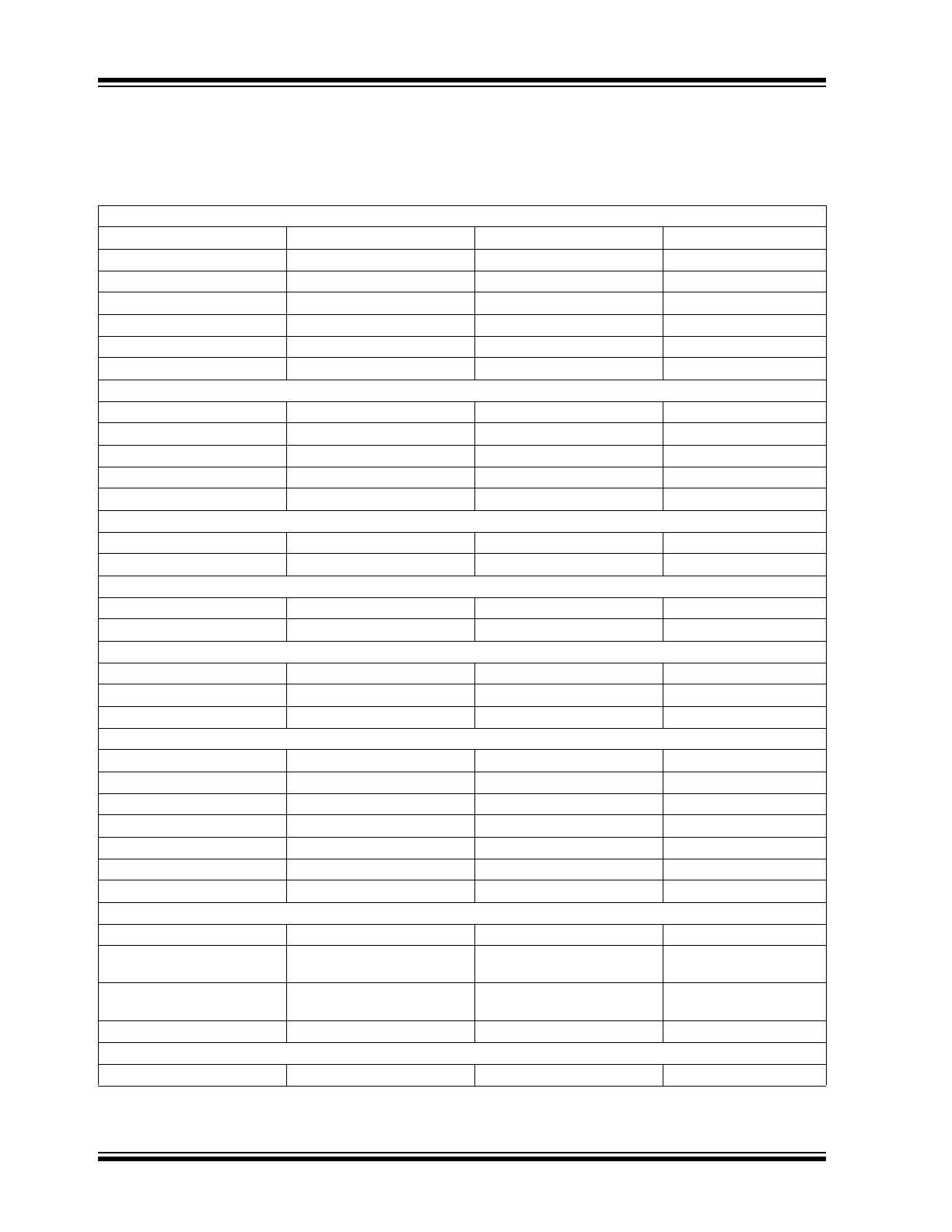
2.0
PIN TABLE
2.1
128-Pin Package
TABLE 2-1:
USB2229/USB2230 128-PIN PACKAGE
CompactFlash INTERFACE (28 Pins)
CF_D0
CF_D1
CF_D2
CF_D3
CF_D4
CF_D5
CF_D6
CF_D7
CF_D8
CF_D9
CF_D10
CF_D11
CF_D12
CF_D13
CF_D14
CF_D15
CF_nIOR
CF_nIOW
CF_IRQ
CF_nRESET
CF_IORDY
CF_nCS0
CF_nCS1
CF_SA0
CF_SA1
CF_SA2
CF_nCD1
CF_nCD2
SmartMedia INTERFACE (17 Pins)
SM_D0
SM_D1
SM_D2
SM_D3
SM_D4
SM_D5
SM_D6
SM_D7
SM_ALE
SM_CLE
SM_nRE
SM_nWE
SM_nWP
SM_nB/R
SM_nCE
SM_nCD
SM_nWPS
Memory Stick INTERFACE (7 Pins)
MS_BS
MS_SDIO/MS_D0
MS_SCLK
MS_INS
MS_D1
MS_D2
MS_D3
SD INTERFACE (7 Pins)
SD_CMD
SD_CLK
SD_DAT0
SD_DAT1
SD_DAT2
SD_DAT3
SD_nWP
USB INTERFACE (10 Pins)
USBDP
USBDM
ATEST
RBIAS
VDD18PLL
VSSPLL
VDDA33
VSSA
XTAL1/CLKIN
XTAL2
MEMORY/IO INTERFACE (27 Pins)
MA0/CLK_SEL0
MA1/CLK_SEL1
MA2/SEL_CLKDRV
MA3/TX_POL
MA4
MA5
MA6
MA7
MA8
MA9
MA10
MA11
MA12
MA13
MA14
MA15
MD0
MD1
MD2
MD3
MD4
MD5
MD6
MD7
nMRD
nMWR
nMCE
MISC (15 Pins)
GPIO1
GPIO2
GPIO3
GPIO4
GPIO5
GPIO6/ROMEN/MA16
GPIO7
GPIO8/
CRD_PWR0
GPIO9
GPIO10/
CRD_PWR1
GPIO11/
CRD_PWR2
GPIO12
nTEST0
nTEST1
nRESET
IrDA (3 PINS)
IR_TXD/TX
IR_RXD/RX
IR_MODE
2005-2016 Microchip Technology Inc.
DS00002252A-page 7
USB2229/USB2230
2.2
128-Pin List Table
DIGITAL, POWER, GROUND & NC (14 Pins)
(5)VDD33
(2)VDD18
(7)VSS
Total 128
TABLE 2-2:
USB2229/USB2230 128-PIN TQFP
Pin #
Name
MA
Pin #
Name
MA
Pin #
Name
MA
Pin #
Name
MA
1
MA13
8
33
CF_D1
8
65
SM_D0
8
97
VSS
-
2
MA14
8
34
CF_D2
8
66
SM_D1
8
98
RBIAS
-
3
VDD33
-
35
CF_D3
8
67
SM_D2
8
99
ATEST
-
4
MA15
8
36
CF_D4
8
68
SM_D3
8
100
VDD33
-
5
MD0
8
37
CF_D5
8
69
SM_D4
8
101
VDD18PLL
-
6
MD1
8
38
CF_D6
8
70
SM_D5
8
102
XTAL1/
CLKIN
-
7
MD2
8
39
CF_D7
8
71
SM_D6
8
103
XTAL2
-
8
MD3
8
40
CF_D8
8
72
SM_D7
8
104
VSSPLL
-
9
MD4
8
41
CF_D9
8
73
SM_ALE
8
105
GPIO9
8
10
MD5
8
42
GPIO8/
CRD_PWR0
8
74
SM_nWP
8
106
VDD18
-
11
MD6
8
43
VDD33
-
75
SM_CLE
8
107
GPIO7
8
12
MD7
8
44
GPIO11/
CRD_PWR2
8
76
SM_nWPS
-
108
VDD33
-
13
nMRD
8
45
CF_D10
8
77
SM_nB/R
-
109
GPIO6/
ROMEN/
MA16
8
14
nMWR
8
46
CF_D11
8
78
SM_nCD
-
110
GPIO5
8
15
VSS
-
47
VSS
-
79
GPIO10/
CRD_PWR1
8
111
GPIO4
8
16
VSS
-
48
CF_D12
8
80
VDD33
-
112
VSS
-
17
nMCE
8
49
VDD18
-
81
SM_nRE
8
113
nRESET
8
18
MS_INS
-
50
CF_D13
8
82
SM_nWE
8
114
GPIO2
8
19
MS_D0/
MS_SDIO
8
51
CF_D14
8
83
SM_nCE
8
115
GPIO1
-
20
MS_D1
8
52
CF_D15
8
84
VSS
-
116
MA0/
CLK_SEL0
8
21
MS_D2
8
53
CF_nCD1
-
85
VSS
-
117
MA1/
CLK_SEL1
8
22
MS_D3
8
54
CF_nCD2
-
86
VSSA
-
118
MA2/
SEL_
CLKDRV
8
23
MS_
SCLK
8
55
CF_IRQ
8
87
USBDM
-
119
MA3/
TX_POL
8
24
MS_BS
8
56
CF_IORDY
8
88
USBDP
-
120
MA4
8
25
SD_nWP
-
57
CF_nIOR
8
89
VDDA33
-
121
MA5
8
26
SD_DAT0
8
58
CF_nIOW
8
90
IR_MODE
8
122
MA6
8
27
SD_DAT1
8
59
CF_nRESET
8
91
IR_RXD/RX
8
123
MA7
8
28
SD_DAT2
8
60
CF_nCS0
8
92
IR_TXD/TX
8
124
MA8
8
TABLE 2-1:
USB2229/USB2230 128-PIN PACKAGE (CONTINUED)

USB2229/USB2230
DS00002252A-page 8
2005-2016 Microchip Technology Inc.
29
SD_DAT3
8
61
CF_nCS1
8
93
GPIO12
8
125
MA9
8
30
SD_CMD
8
62
CF_SA0
8
94
GPIO3
8
126
MA10
8
31
SD_CLK
-
63
CF_SA1
8
95
nTEST1
-
127
MA11
8
32
CF_D0
8
64
CF_SA2
-
96
nTEST0
-
128
MA12
8
TABLE 2-2:
USB2229/USB2230 128-PIN TQFP (CONTINUED)
Pin #
Name
MA
Pin #
Name
MA
Pin #
Name
MA
Pin #
Name
MA
USB2229/USB2230
DS000022
52A-page 9
2005-
2016 Microchip T
e
chnolo
g
y Inc.
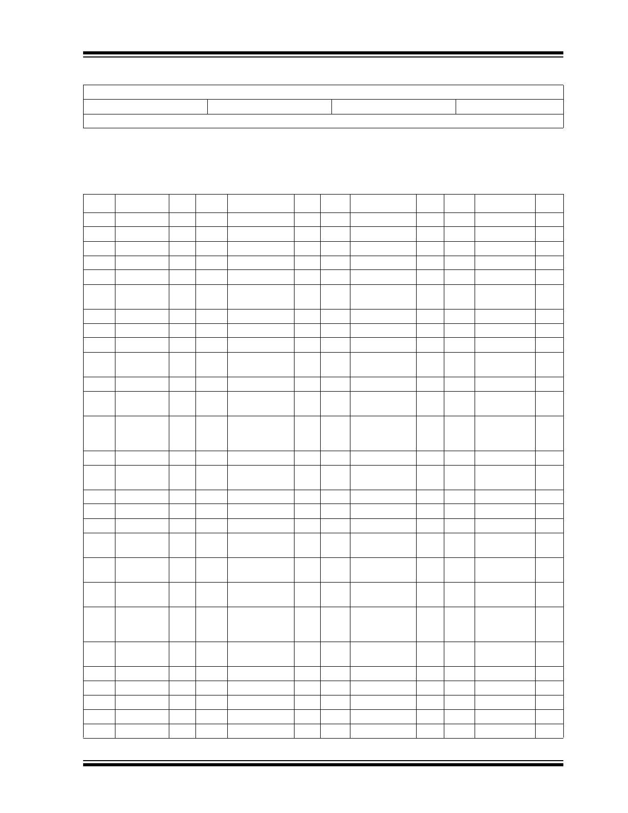
3.0
BLOCK DIAGRAM
D
a
ta
B
u
ss
USB 2.0 PHY
( Transciever )
FAST 8051
CPU CORE
7 pi
ns
Configuration and Control
Clock Generation
X
T
A
L
SIE
( Serial Interface Engine )
Program Memory/ IO
Bus
Interrupt Controller
Latch phase 0, 2
SIE
Latch phase 3
8051
Latch phase 1
FMC
32 Bit
Osc
Address
X
D
AT
A &
SF
R
A
ddr
es
s and D
a
ta
bus
se
s
Auto address generators
Ad
dr
e
ss
M
U
X
SIE Control Regs
Address
Address
EP0RX_BC
RAMRD_A/B
EP0TX_BC
RAMWR_A/B
32 bit 15MHz Data Bus
CLOCKOUT
24 MHz
A
d
d
res
s R
e
g
ist
er
2.25KB
SRAM
12K Byte
Scratchpad
SRAM
#LOCKED
#LOCKED
Memory
Cards
Scratchpad
SRAM (768 Byte)
F
M
C Da
ta
M
U
X
ECC
Control/
Status
SD
Controller
SD/MMC
Flash Media
Controllers
(FMC)
Control/
Status
MS
Controller
MS/HS MS/MS PRO
Control/
Status
SM
Controller
SM/SSFDC
Control/
Status
CF
Controller
CF
Control/
Status
CRC
MEM/IO Bus 29pins
DATA
DATA
DATA
DATA
CRC
EP1TX_BC
Address
Address
Flash Media DMA Unit
76K ROM
ROMEN
IrDA + 128Byte FIFO
Address
RAMRD_C/D
RAMWR_C/D
Address
Address
Address
EP1RX_BC
64 Bytes EP0TX
64 Bytes EP0RX
64 Bytes EP1TX
64 Bytes EP1RX
512 Bytes EP2 TX/RX Buffer A
512 Bytes EP2 TX/RX Buffer B
512 Bytes EP3 TX/RX Buffer A
512 Bytes EP3 TX/RX Buffer B
IR
Transceiver
60MHz
Data @ 32 bit
15MHz
GPIO
12 pins
PWR_FET0
PWR_FET1
PWR_FET2
GPIO11/CRD_PWR2
GPIO10/CRD_PWR1
GPIO8/CRD_PWR0
USB2229/USB2230
DS00002252A-page 10
2005-2016 Microchip Technology Inc.
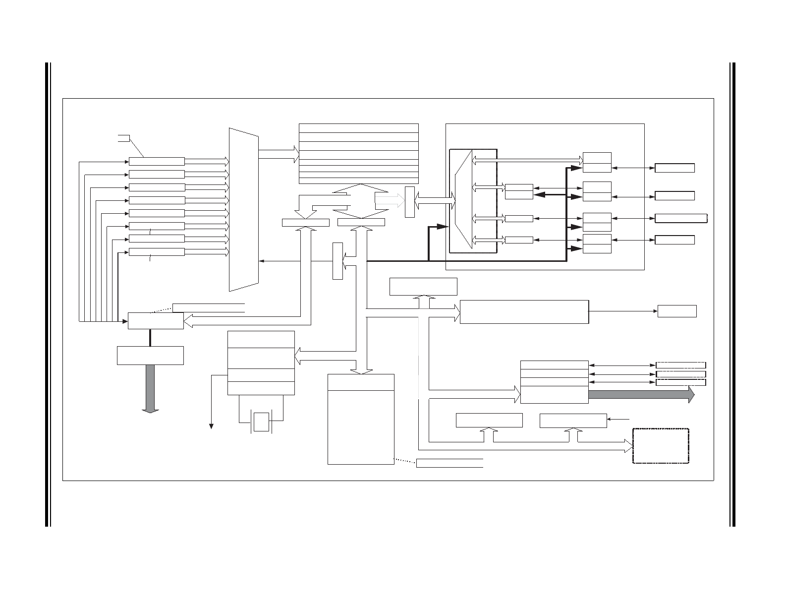
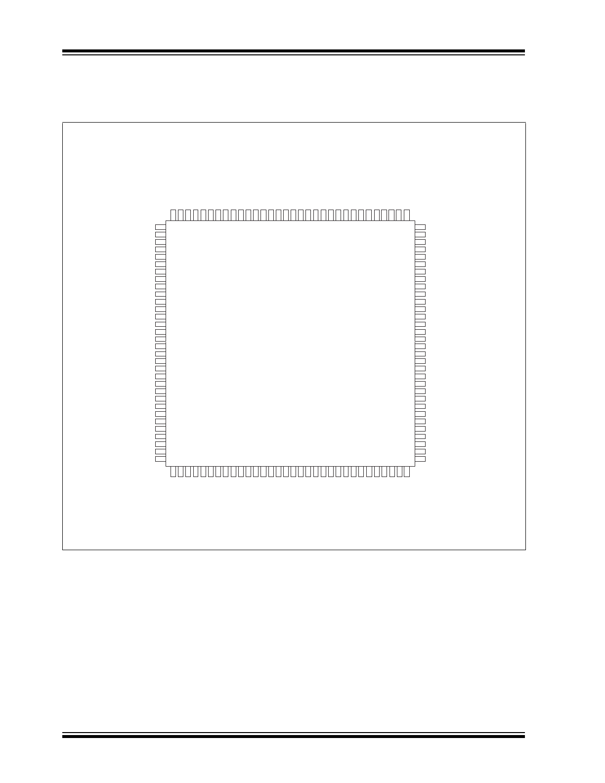
4.0
PIN CONFIGURATION
FIGURE 4-1:
USB2229/USB2230 128-PIN TQFP
MA
1
2
MA
1
1
MA
1
0
MA
9
MA
8
MA
7
MA
6
MA
5
MA
4
M
A
3/TX_POL
M
A
2/SEL_CLKDR
V
M
A
1/CLK_SEL1
M
A
0/CLK_SEL0
GPIO1
GPIO2
nRESET
VS
S
GP
IO
4
GP
IO
5
G
P
IO
6
/R
O
M
E
N/MA16
VD
D
3
3
GP
IO
7
VD
D
1
8
GP
IO
9
V
SSP
L
L
XT
A
L
2
XT
A
L
1/CLKIN
V
D
D
18P
LL
VD
D
3
3
AT
E
S
T
RB
IA
S
VS
S
CF
_
D
1
CF
_
D
2
CF
_
D
3
CF
_
D
4
CF
_
D
5
CF
_
D
6
CF
_
D
7
CF
_
D
8
CF
_
D
9
GPIO8/CRD_PWR0
VD
D
3
3
GPIO1
1/CRD_PWR2
C
F
_D
10
C
F
_D
11
VS
S
C
F
_D
12
VD
D
1
8
C
F
_D
13
C
F
_D
14
C
F
_D
15
CF
_
n
C
D1
CF
_
n
C
D2
CF
_
IRQ
CF
_
IO
R
D
Y
C
F
_nI
O
R
C
F
_nI
O
W
C
F
_nR
E
S
E
T
C
F
_nC
S
0
C
F
_nC
S
1
CF
_
S
A
0
CF
_
S
A
1
CF
_
S
A
2
USB2230
32
64
96
1
MA13
MA14
VDD33
MA15
MD0
MD1
MD2
MD3
MD4
MD5
MD6
MD7
nMRD
nMWR
VSS
VSS
nMCE
MS_INS
MS_D0/MS_SDIO
MS_D1
MS_D2
MS_D3
MS_SCLK
MS_BS
SD_nWP
SD_DAT0
SD_DAT1
SD_DAT2
SD_DAT3
SD_CMD
SD_CLK
CF_D0
nTEST0
nTEST1
GPIO3
GPIO12
IR_TXD/TX
IR_RXD/RX
IR_MODE
VDDA33
USBDP
USBDM
VSSA
VSS
VSS
SM_nCE
SM_nWE
SM_nRE
VDD33
GPIO10/CRD_PWR1
SM_nCD
SM_nB/R
SM_nWPS
SM_CLE
SM_nWP
SM_ALE
SM_D7
SM_D6
SM_D5
SM_D4
SM_D3
SM_D2
SM_D1
SM_D0
2005-2016 Microchip Technology Inc.
DS00002252A-page 1
IrDA Controller
• IrDA v1.1 FIR and SIR Compliant Controller, with
9.6K, 19.2K, 38.4K, 57.6K, 115.2K, 0.576Mbps,
1.152Mpbs and 4Mbps data rate support.
Flash Media Controller
• Complete System Solution for interfacing Smart-
Media
™
(SM) or xD Picture Card
™
(xD)
1
, Memory
Stick
™
(MS), High Speed Memory Stick (HSMS),
Memory Stick PRO (MSPRO), MS Duo
™
, Secure
Digital (SD), High Speed SD, Mini-Secure Digital
(Mini-SD), TransFlash (SD), MultiMediaCard
™
(MMC), Reduced Size MultiMediaCard (RS-
MMC), NAND Flash, Compact Flash
™
(CF) and
CF Ultra
™
I & II, and CF form-factor ATA hard
drives to Hi-Speed USB
- Supports USB Bulk Only Mass Storage Com-
pliant Bootable BIOS
• Support for simultaneous operation of all above
devices. (only one at a time of each of the follow-
ing groups supported: CF or ATA drive, SM or XD
or NAND, SD or MMC)
• On-Chip 4-Bit High Speed Memory Stick and MS
PRO Hardware Circuitry
• On-Chip firmware reads and writes High Speed
Memory Stick and MS PRO
• 1-bit ECC correction performed in hardware for
maximum efficiency
• Hardware support for SD Security Command
Extensions
• On-chip power FETs with short circuit protection
for supplying flash media card power
• USB Bus Power Certified
• 3.3 Volt I/O with 5V input tolerance on VBUS/
GPIO3
• Complete USB Specification 2.0 Compatibility for
Bus Powered Operation
- Includes Hi-Speed USB Transceiver
- A Bi-directional Control and two Bi-directional
Bulk Endpoints are provided.
• 8051 8 bit microprocessor
- Provides low speed control functions
- 30 Mhz execution speed at 1 clock per
instruction cycle average
- 12K Bytes of internal SRAM for general pur-
pose scratchpad
- 768 Bytes of internal SRAM for general pur-
pose scratchpad or program execution while
re-flashing external ROM
- Two, Double Buffered Bulk Endpoints
- Two, Bi-directional 512 Byte Buffers for Bulk
Endpoints
- 64 Byte RX Control Endpoint Buffer
- 64 Byte TX Control Endpoint Buffer
• Internal or External Program Memory Interface
- 76K Byte Internal Code Space or Optional
128K Byte External Code Space using Flash,
SRAM or EPROM memory.
• On Board 24Mhz Crystal Driver Circuit
• Can be clocked by 48MHz external source
• On-Chip 1.8V Regulator for Low Power Core
Operation
• Internal PLL for 480Mhz Hi-Speed USB Sampling,
Configurable MCU clock
• Supports firmware upgrade via USB bus if “boot
block” Flash program memory is used
• 12 GPIOs for special function use: LED indica-
tors, button inputs, power control to memory
devices, etc.
- Inputs capable of generating interrupts with
either edge sensitivity
• Attribute bit controlled features:
- Activity LED polarity/operation/blink rate
- Full or Partial Card compliance checking
- Bus or Self Powered
- LUN configuration and assignment
- Write Protect Polarity
- SmartDetach - Detach from USB when no
Card Inserted for Notebook apps
- Cover Switch operation for xD compliance
- Inquiry Command operation
- SD Write Protect operation
- Older CF card support
- Force USB 1.1 reporting
- Internal or External Power FET operation
• Compatible with Microsoft WinXP, WinME, Win2K
SP3, Apple OS10, Softconnex, and Linux Multi-
LUN Mass Storage Class Drivers
• Win2K, Win98/98SE and Apple OS8.6 and OS9
Multi-LUN Mass Storage Class Drivers available
from Microchip
• 128-Pin TQFP RoHS Compliant package (1.0mm
height, 14mmx14mm footprint)
1.xD Picture Card not applicable to USB2229.
USB2229/USB2230
5th Generation Hi-Speed USB Flash Media
and IrDA Controller with Integrated Card Power FETs
USB2229/USB2230
DS00002252A-page 2
2005-2016 Microchip Technology Inc.
TO OUR VALUED CUSTOMERS
It is our intention to provide our valued customers with the best documentation possible to ensure successful use of your Microchip
products. To this end, we will continue to improve our publications to better suit your needs. Our publications will be refined and
enhanced as new volumes and updates are introduced.
If you have any questions or comments regarding this publication, please contact the Marketing Communications Department via
E-mail at
docerrors@microchip.com
. We welcome your feedback.
Most Current Data Sheet
To obtain the most up-to-date version of this data sheet, please register at our Worldwide Web site at:
http://www.microchip.com
You can determine the version of a data sheet by examining its literature number found on the bottom outside corner of any page.
The last character of the literature number is the version number, (e.g., DS30000000A is version A of document DS30000000).
Errata
An errata sheet, describing minor operational differences from the data sheet and recommended workarounds, may exist for cur-
rent devices. As device/documentation issues become known to us, we will publish an errata sheet. The errata will specify the
revision of silicon and revision of document to which it applies.
To determine if an errata sheet exists for a particular device, please check with one of the following:
• Microchip’s Worldwide Web site;
http://www.microchip.com
• Your local Microchip sales office (see last page)
When contacting a sales office, please specify which device, revision of silicon and data sheet (include -literature number) you are
using.
Customer Notification System
Register on our web site at
www.microchip.com
to receive the most current information on all of our products.
2005-2016 Microchip Technology Inc.
DS00002252A-page 3
USB2229/USB2230
Table of Contents
1.0 General Description ........................................................................................................................................................................ 4
2.0 Pin Table ......................................................................................................................................................................................... 6
3.0 Block Diagram ................................................................................................................................................................................. 9
4.0 Pin Configuration .......................................................................................................................................................................... 10
5.0 Pin Descriptions ............................................................................................................................................................................ 11
6.0 DC Parameters ............................................................................................................................................................................. 18
7.0 Package Information ..................................................................................................................................................................... 22
8.0 GPIO Usage .................................................................................................................................................................................. 23
Appendix A: Data Sheet Revision History ........................................................................................................................................... 24
The Microchip Web Site ...................................................................................................................................................................... 25
Customer Change Notification Service ............................................................................................................................................... 25
Customer Support ............................................................................................................................................................................... 25
Product Identification System ............................................................................................................................................................. 26
USB2229/USB2230
DS00002252A-page 4
2005-2016 Microchip Technology Inc.
1.0
GENERAL DESCRIPTION
The USB2229/USB2230 is a Hi-Speed USB IrDA and Bulk Only Mass Storage Class Peripheral Controller. The Bulk
Only Mass Storage Class Peripheral Controller supports CompactFlash (CF) in True IDE Mode only, SmartMedia (SM),
Memory Stick (MS) including both serial and parallel interface and Secure Digital/MultiMediaCard (SD/MMC) flash
memory devices. It provides a single chip solution for the most popular flash memory cards in the market. In addition,
the IrDA controller consists of the Microchip IrCC block, which includes a Synchronous Communications Engine (SCE).
The IrCC SCE supports FIR and SIR IrDA. The IrCC offers flexible signal routing and programmable output control
through the Raw mode interface, General Purpose Data pins and Output Multiplexer. Chip-level address decoding is
required to access the IrCC register set.
The device consists of a USB2.0 PHY and SIE, buffers, Fast 8051 microprocessor with expanded scratchpad, and pro-
gram SRAM, and IrDA, CF, MS, SM and SD controllers. The SD controller supports both SD and MMC devices.
Provisions for external Flash Memory up to 128K bytes for program storage is provided (note: when Bank switching is
enabled the upper 64K will map into the 8051 ROM space, otherwise, only the first 64K bytes is used).
12K bytes of scratchpad SRAM and 768Bytes of program SRAM are also provided.
Twelve GPIO pins are provided for indicators, external serial EEPROM for OEM ID and system configuration informa-
tion, and other special functions.
Internal power FETs are provided to directly supply power to the xD/SM, MMC/SD and MS/MSPro cards.
The internal ROM program is capable of implementing any combination of single or multi-LUN CF/SD/MMC/SM/MS
reader functions with individual card power control and activity indication. Microchip also provides licenses** for Win98
and Win2K drivers and setup utilities. Note: Please check with Microchip for precise features and capabilities for the
current ROM code release.
1.1
Acronyms
SM: SmartMedia
SMC: SmartMedia
Controller
FM:
Flash Media
FMC: Flash
Media
Controller
CF: Compact
Flash
CFC: CompactFlash
Controller
SD: Secure
Digital
SDC: Secure
Digital
Controller
MMC: MultiMediaCard
MS: Memory
Stick
MSC:
Memory Stick Controller
TPC:
Transport Protocol Code.
ECC:
Error Checking and Correcting
CRC:
Cyclic Redundancy Checking
1.2
Reference Documents
1.
SmartMedia
™
Electrical Specification Version 1.30
2.
SmartMedia
™
Physical Format Specifications Version 1.30
3.
SmartMedia
™
Logical Format Specifications Version 1.20
4.
SMIL (SmartMedia Interface Library) Software Edition Version 1.00, Toshiba Corporation, 01, July, 2000
5.
SMIL (SmartMedia Interface Library) Hardware Edition Version 1.00, Toshiba Corporation, 01, July, 2000
6.
MultiMediaCard System Specification Version 2.2
7.
SD Memory Card Specifications, Part 1, Physical Layer Specification Version 1.10, April 2003, SD Group
8.
SD Memory Card Specifications, Part 2, File System Specification Version 1.01, April 15
th
, 2001, SD Group
9.
SD Memory Card Specifications, Part 3, Security Specification Version 1.01, April 15
th
, 2001, SD Group
2005-2016 Microchip Technology Inc.
DS00002252A-page 5
USB2229/USB2230
10. SD Card Specification, Part E1, Secure Digital Input/Output (SDIO) card Specification, Version 1.00, October
2001, SD Group.
11. Memory Stick Standard Excerption from Format Specification v1.3, July, 2000, Sony Corporation.
12. Memory Stick Standard Format Specifications ver 2.0 (Memory Stick PRO). Tentative Release 0.81, February,
2002
13. CompactFlash Specification Rev 1.4
14. CF+ & CF Specification Rev. ATA-5 Draft 0.2
15. Universal Serial Bus Specification Rev 2.0
16. Samsung K9K2G08Q0M Data Sheet
17. xD Picture Card, Card Specification Version 1.10 (Jan 31, 2004)
18. xD Picture Card, Format Specification Version 1.10 (Jan 31, 2004)
19. xD Picture Card, Host Guideline Version 1.10 (Jan 31, 2004)
20. xD Picture Card, Compliance Guideline Version 1.10 (Jan 31, 2004)
USB2229/USB2230
DS00002252A-page 6
2005-2016 Microchip Technology Inc.
2.0
PIN TABLE
2.1
128-Pin Package
TABLE 2-1:
USB2229/USB2230 128-PIN PACKAGE
CompactFlash INTERFACE (28 Pins)
CF_D0
CF_D1
CF_D2
CF_D3
CF_D4
CF_D5
CF_D6
CF_D7
CF_D8
CF_D9
CF_D10
CF_D11
CF_D12
CF_D13
CF_D14
CF_D15
CF_nIOR
CF_nIOW
CF_IRQ
CF_nRESET
CF_IORDY
CF_nCS0
CF_nCS1
CF_SA0
CF_SA1
CF_SA2
CF_nCD1
CF_nCD2
SmartMedia INTERFACE (17 Pins)
SM_D0
SM_D1
SM_D2
SM_D3
SM_D4
SM_D5
SM_D6
SM_D7
SM_ALE
SM_CLE
SM_nRE
SM_nWE
SM_nWP
SM_nB/R
SM_nCE
SM_nCD
SM_nWPS
Memory Stick INTERFACE (7 Pins)
MS_BS
MS_SDIO/MS_D0
MS_SCLK
MS_INS
MS_D1
MS_D2
MS_D3
SD INTERFACE (7 Pins)
SD_CMD
SD_CLK
SD_DAT0
SD_DAT1
SD_DAT2
SD_DAT3
SD_nWP
USB INTERFACE (10 Pins)
USBDP
USBDM
ATEST
RBIAS
VDD18PLL
VSSPLL
VDDA33
VSSA
XTAL1/CLKIN
XTAL2
MEMORY/IO INTERFACE (27 Pins)
MA0/CLK_SEL0
MA1/CLK_SEL1
MA2/SEL_CLKDRV
MA3/TX_POL
MA4
MA5
MA6
MA7
MA8
MA9
MA10
MA11
MA12
MA13
MA14
MA15
MD0
MD1
MD2
MD3
MD4
MD5
MD6
MD7
nMRD
nMWR
nMCE
MISC (15 Pins)
GPIO1
GPIO2
GPIO3
GPIO4
GPIO5
GPIO6/ROMEN/MA16
GPIO7
GPIO8/
CRD_PWR0
GPIO9
GPIO10/
CRD_PWR1
GPIO11/
CRD_PWR2
GPIO12
nTEST0
nTEST1
nRESET
IrDA (3 PINS)
IR_TXD/TX
IR_RXD/RX
IR_MODE
2005-2016 Microchip Technology Inc.
DS00002252A-page 7
USB2229/USB2230
2.2
128-Pin List Table
DIGITAL, POWER, GROUND & NC (14 Pins)
(5)VDD33
(2)VDD18
(7)VSS
Total 128
TABLE 2-2:
USB2229/USB2230 128-PIN TQFP
Pin #
Name
MA
Pin #
Name
MA
Pin #
Name
MA
Pin #
Name
MA
1
MA13
8
33
CF_D1
8
65
SM_D0
8
97
VSS
-
2
MA14
8
34
CF_D2
8
66
SM_D1
8
98
RBIAS
-
3
VDD33
-
35
CF_D3
8
67
SM_D2
8
99
ATEST
-
4
MA15
8
36
CF_D4
8
68
SM_D3
8
100
VDD33
-
5
MD0
8
37
CF_D5
8
69
SM_D4
8
101
VDD18PLL
-
6
MD1
8
38
CF_D6
8
70
SM_D5
8
102
XTAL1/
CLKIN
-
7
MD2
8
39
CF_D7
8
71
SM_D6
8
103
XTAL2
-
8
MD3
8
40
CF_D8
8
72
SM_D7
8
104
VSSPLL
-
9
MD4
8
41
CF_D9
8
73
SM_ALE
8
105
GPIO9
8
10
MD5
8
42
GPIO8/
CRD_PWR0
8
74
SM_nWP
8
106
VDD18
-
11
MD6
8
43
VDD33
-
75
SM_CLE
8
107
GPIO7
8
12
MD7
8
44
GPIO11/
CRD_PWR2
8
76
SM_nWPS
-
108
VDD33
-
13
nMRD
8
45
CF_D10
8
77
SM_nB/R
-
109
GPIO6/
ROMEN/
MA16
8
14
nMWR
8
46
CF_D11
8
78
SM_nCD
-
110
GPIO5
8
15
VSS
-
47
VSS
-
79
GPIO10/
CRD_PWR1
8
111
GPIO4
8
16
VSS
-
48
CF_D12
8
80
VDD33
-
112
VSS
-
17
nMCE
8
49
VDD18
-
81
SM_nRE
8
113
nRESET
8
18
MS_INS
-
50
CF_D13
8
82
SM_nWE
8
114
GPIO2
8
19
MS_D0/
MS_SDIO
8
51
CF_D14
8
83
SM_nCE
8
115
GPIO1
-
20
MS_D1
8
52
CF_D15
8
84
VSS
-
116
MA0/
CLK_SEL0
8
21
MS_D2
8
53
CF_nCD1
-
85
VSS
-
117
MA1/
CLK_SEL1
8
22
MS_D3
8
54
CF_nCD2
-
86
VSSA
-
118
MA2/
SEL_
CLKDRV
8
23
MS_
SCLK
8
55
CF_IRQ
8
87
USBDM
-
119
MA3/
TX_POL
8
24
MS_BS
8
56
CF_IORDY
8
88
USBDP
-
120
MA4
8
25
SD_nWP
-
57
CF_nIOR
8
89
VDDA33
-
121
MA5
8
26
SD_DAT0
8
58
CF_nIOW
8
90
IR_MODE
8
122
MA6
8
27
SD_DAT1
8
59
CF_nRESET
8
91
IR_RXD/RX
8
123
MA7
8
28
SD_DAT2
8
60
CF_nCS0
8
92
IR_TXD/TX
8
124
MA8
8
TABLE 2-1:
USB2229/USB2230 128-PIN PACKAGE (CONTINUED)
USB2229/USB2230
DS00002252A-page 8
2005-2016 Microchip Technology Inc.
29
SD_DAT3
8
61
CF_nCS1
8
93
GPIO12
8
125
MA9
8
30
SD_CMD
8
62
CF_SA0
8
94
GPIO3
8
126
MA10
8
31
SD_CLK
-
63
CF_SA1
8
95
nTEST1
-
127
MA11
8
32
CF_D0
8
64
CF_SA2
-
96
nTEST0
-
128
MA12
8
TABLE 2-2:
USB2229/USB2230 128-PIN TQFP (CONTINUED)
Pin #
Name
MA
Pin #
Name
MA
Pin #
Name
MA
Pin #
Name
MA
USB2229/USB2230
DS000022
52A-page 9
2005-
2016 Microchip T
e
chnolo
g
y Inc.
3.0
BLOCK DIAGRAM
D
a
ta
B
u
ss
USB 2.0 PHY
( Transciever )
FAST 8051
CPU CORE
7 pi
ns
Configuration and Control
Clock Generation
X
T
A
L
SIE
( Serial Interface Engine )
Program Memory/ IO
Bus
Interrupt Controller
Latch phase 0, 2
SIE
Latch phase 3
8051
Latch phase 1
FMC
32 Bit
Osc
Address
X
D
AT
A &
SF
R
A
ddr
es
s and D
a
ta
bus
se
s
Auto address generators
Ad
dr
e
ss
M
U
X
SIE Control Regs
Address
Address
EP0RX_BC
RAMRD_A/B
EP0TX_BC
RAMWR_A/B
32 bit 15MHz Data Bus
CLOCKOUT
24 MHz
A
d
d
res
s R
e
g
ist
er
2.25KB
SRAM
12K Byte
Scratchpad
SRAM
#LOCKED
#LOCKED
Memory
Cards
Scratchpad
SRAM (768 Byte)
F
M
C Da
ta
M
U
X
ECC
Control/
Status
SD
Controller
SD/MMC
Flash Media
Controllers
(FMC)
Control/
Status
MS
Controller
MS/HS MS/MS PRO
Control/
Status
SM
Controller
SM/SSFDC
Control/
Status
CF
Controller
CF
Control/
Status
CRC
MEM/IO Bus 29pins
DATA
DATA
DATA
DATA
CRC
EP1TX_BC
Address
Address
Flash Media DMA Unit
76K ROM
ROMEN
IrDA + 128Byte FIFO
Address
RAMRD_C/D
RAMWR_C/D
Address
Address
Address
EP1RX_BC
64 Bytes EP0TX
64 Bytes EP0RX
64 Bytes EP1TX
64 Bytes EP1RX
512 Bytes EP2 TX/RX Buffer A
512 Bytes EP2 TX/RX Buffer B
512 Bytes EP3 TX/RX Buffer A
512 Bytes EP3 TX/RX Buffer B
IR
Transceiver
60MHz
Data @ 32 bit
15MHz
GPIO
12 pins
PWR_FET0
PWR_FET1
PWR_FET2
GPIO11/CRD_PWR2
GPIO10/CRD_PWR1
GPIO8/CRD_PWR0
USB2229/USB2230
DS00002252A-page 10
2005-2016 Microchip Technology Inc.
4.0
PIN CONFIGURATION
FIGURE 4-1:
USB2229/USB2230 128-PIN TQFP
MA
1
2
MA
1
1
MA
1
0
MA
9
MA
8
MA
7
MA
6
MA
5
MA
4
M
A
3/TX_POL
M
A
2/SEL_CLKDR
V
M
A
1/CLK_SEL1
M
A
0/CLK_SEL0
GPIO1
GPIO2
nRESET
VS
S
GP
IO
4
GP
IO
5
G
P
IO
6
/R
O
M
E
N/MA16
VD
D
3
3
GP
IO
7
VD
D
1
8
GP
IO
9
V
SSP
L
L
XT
A
L
2
XT
A
L
1/CLKIN
V
D
D
18P
LL
VD
D
3
3
AT
E
S
T
RB
IA
S
VS
S
CF
_
D
1
CF
_
D
2
CF
_
D
3
CF
_
D
4
CF
_
D
5
CF
_
D
6
CF
_
D
7
CF
_
D
8
CF
_
D
9
GPIO8/CRD_PWR0
VD
D
3
3
GPIO1
1/CRD_PWR2
C
F
_D
10
C
F
_D
11
VS
S
C
F
_D
12
VD
D
1
8
C
F
_D
13
C
F
_D
14
C
F
_D
15
CF
_
n
C
D1
CF
_
n
C
D2
CF
_
IRQ
CF
_
IO
R
D
Y
C
F
_nI
O
R
C
F
_nI
O
W
C
F
_nR
E
S
E
T
C
F
_nC
S
0
C
F
_nC
S
1
CF
_
S
A
0
CF
_
S
A
1
CF
_
S
A
2
USB2230
32
64
96
1
MA13
MA14
VDD33
MA15
MD0
MD1
MD2
MD3
MD4
MD5
MD6
MD7
nMRD
nMWR
VSS
VSS
nMCE
MS_INS
MS_D0/MS_SDIO
MS_D1
MS_D2
MS_D3
MS_SCLK
MS_BS
SD_nWP
SD_DAT0
SD_DAT1
SD_DAT2
SD_DAT3
SD_CMD
SD_CLK
CF_D0
nTEST0
nTEST1
GPIO3
GPIO12
IR_TXD/TX
IR_RXD/RX
IR_MODE
VDDA33
USBDP
USBDM
VSSA
VSS
VSS
SM_nCE
SM_nWE
SM_nRE
VDD33
GPIO10/CRD_PWR1
SM_nCD
SM_nB/R
SM_nWPS
SM_CLE
SM_nWP
SM_ALE
SM_D7
SM_D6
SM_D5
SM_D4
SM_D3
SM_D2
SM_D1
SM_D0