
2009-2013 Microchip Technology Inc.
DS22191E-page 1
MCP73123/223
Features:
• Complete Linear Charge Management Controller:
- Integrated Input Overvoltage Protection (OVP)
- Integrated Pass Transistor
- Integrated Current Sense
- Integrated Reverse Discharge Protection
• Constant Current/Constant Voltage Operation
with Thermal Regulation
• 4.15V Undervoltage Lockout (UVLO)
• 18V Absolute Maximum Input with OVP:
- 6.5V - MCP73123
- 13V - MCP73223
• High Accuracy Preset Voltage Regulation
Through Full Temperature Range (-5°C to +55°C):
- +0.5% - MCP73123
- +0.6% - MCP73223
• Battery Charge Voltage Options:
- 3.6V - MCP73123
- 7.2V - MCP73223
• Resistor Programmable Fast Charge Current:
- 130 mA - 1100 mA
• Preconditioning of Deeply Depleted Cells:
- Available Options: 10% or Disable
• Integrated Precondition Timer:
- 32 Minutes or Disable
• Automatic End-of-Charge Control:
- Selectable Minimum Current Ratio:
5%, 7.5%, 10% or 20%
- Elapse Safety Timer: 4 HR, 6 HR, 8 HR or
Disable
• Automatic Recharge:
- Available Options: 95% or Disable
• Factory Preset Charge Status Output:
- On/Off or Flashing
• Soft Start
• Temperature Range: -40°C to +85°C
• Packaging: DFN-10 (3 mm x 3 mm)
Applications:
• Low-Cost LiFePO
4
Battery Chargers
• Power Tools
• Toys
• Backup Energy Storage Solutions
Description:
The MCP73123/223 is a highly integrated Lithium Iron
Phosphate (LiFePO
4
) battery charge management
controller for use in space-limited and cost-sensitive
applications. The MCP73123/223 provides specific
charge algorithms for LiFePO
4
batteries to achieve
optimal capacity and safety in the shortest charging
time possible. Along with its small physical size, the low
number of external components makes the
MCP73123/223 ideally suitable for various
applications. The absolute maximum voltage, up to
18V, allows the use of MCP73123/223 in harsh
environments, such as low cost AC adapter or voltage
spikes from plugging/unplugging.
The MCP73123/223 employs a constant current/
constant voltage charge algorithm. The 3.6V per cell
factory preset reference voltage simplifies design with
2V preconditioning threshold. The fast charge,
constant current value is set with one external resistor
from 130 mA to 1100 mA. The MCP73123/223 also
limits the charge current based on die temperature
during high power or high ambient conditions. This
thermal regulation optimizes the charge cycle time
while maintaining device reliability.
The PROG pin of the MCP73123/223 also serves as
the enable pin. When high impedance is applied, the
MCP73123/223 will be in Standby mode.
The MCP73123/223 is fully specified over the ambient
temperature range of -40°C to +85°C. The MCP73123/
223 is available in a 10 lead DFN package.
Package Types (Top View)
MCP73123/223
3x3 DFN *
V
BAT
V
DD
V
BAT
V
SS
V
SS
1
2
3
4
10
9
8
7 STAT
PROG
V
DD
* Includes Exposed Thermal Pad (EP); see
Table 3-1
.
EP
11
NC 5
6 NC
Lithium Iron Phosphate (LiFePO
4
) Battery Charge
Management Controller with Input Overvoltage Protection
MCP73123/223
DS22191E-page 2
2009-2013 Microchip Technology Inc.
Typical Application
TABLE 1:
AVAILABLE FACTORY PRESET OPTIONS
TABLE 2:
STANDARD SAMPLE OPTIONS
Charge
Voltage
OVP
Preconditioning
Charge Current
Preconditioning
Threshold
Precondition
Timer
Elapse
Timer
End-of-
Charge
Control
Automatic
Recharge
Output
Status
3.6V
6.5V
Disable/10%
2V
Disable /
32 Minimum
Disable/4 hr./
6 hr./8 hr.
5%/7.5%/
10%/20%
No /
Yes
Type 1/
Type 2
7.2V
13V
Disable/10%
4V
Disable /
32 Minimum
Disable/4 hr./
6 hr./8 hr.
5%/7.5%/
10%/20%
No /
Yes
Type 1/
Type 2
Note 1:
I
REG
: Regulated fast charge current.
2:
V
REG
: Regulated charge voltage.
3:
I
PREG
/I
REG
: Preconditioning charge current; ratio of regulated fast charge current.
4:
I
TERM
/I
REG
: End-of-Charge control; ratio of regulated fast charge current.
5:
V
RTH
/V
REG
: Recharge threshold; ratio of regulated battery voltage, 0% or 95%. 0% = Disabled.
6:
V
PTH
/V
REG
: Preconditioning threshold voltage.
7:
Type 1: On/Off; Type 2: Flashing. Please refer to
Table 5-2
.
Part
Number
V
REG
OVP I
PREG
/I
REG
Precharge
Timer
Elapse
Timer
I
TERM
/I
REG
Auto Recharge
Threshold
(0% = Disabled)
V
PTH
/V
REG
Output
Status
MCP73123-22S/MF
3.6V
6.5V
10%
32 Min.
6 hr.
10%
95%
2V
Type 1
MCP73123-22A/MF
3.6V
6.5V
10%
32 Min.
6 hr.
10%
0%
2V
Type 1
MCP73223-C2S/MF
7.2V
13V
10%
32 Min.
6 hr.
10%
95%
4V
Type 1
MCP73223-C2A/MF
7.2V
13V
10%
32 Min.
6 hr.
10%
0%
4V
Type 1
Note 1:
Customers should contact their distributor, representatives or field application engineer (FAE) for support and samples.
Local sales offices are also available to help customers. A listing of sales offices and locations is included in the back of
this document. Technical support is available through the web site at: http//support.microchip.com.
2:
Contact your local Microchip sales office for alternative device options.
STAT
V
DD
NC
5
3
1
2
PROG
8
7
9
10
4.7 µF
+
-
1-Cell
LiFePO
4
Battery
NC
6
4
1 k
V
DD
V
BAT
V
BAT
V
SS
V
SS
4.7 µF
1.15 k
MCP73123 Typical Application
AC-DC Adapter
2009-2013 Microchip Technology Inc.
DS22191E-page 3
MCP73123/223
Functional Block Diagram
REFERENCE,
BIAS, UVLO,
AND SHDN
VREF (1.21V)
STAT
PROG
VBAT
VSS
DIRECTION
CONTROL
PRECONDITION
+
-
TERM
+
-
+
-
CA
CHARGE
+
-
+
-
VA
+
-
CURRENT
LIMIT
CHARGE
CONTROL,
TIMER,
AND
STATUS
LOGIC
VREF
VOREG
VOREG
UVLO
VDD
Input OverVP
VDD
+
-
6.5V/13V
Thermal Regulation
TSD
+
-
110 C
*Recharge
VBAT
+
-
95% VREG
*Only available on selected options
G=0.001
MCP73123/223
DS22191E-page 4
2009-2013 Microchip Technology Inc.
1.0
ELECTRICAL
CHARACTERISTICS
Absolute Maximum Ratings†
V
DD
................................................................................18.0V
V
PROG
..............................................................................6.0V
All Inputs and Outputs w.r.t. V
SS
............... -0.3 to (V
DD
+0.3)V
Maximum Junction Temperature, T
J
............Internally Limited
Storage temperature .....................................-65°C to +150°C
ESD protection on all pins
Human Body Model (1.5 k
in Series with 100 pF)4 kV
Machine Model (200pF, No Series Resistance) ..............300V
† Notice: Stresses above those listed under “Maximum
Ratings” may cause permanent damage to the device. This is
a stress rating only and functional operation of the device at
those or any other conditions above those indicated in the
operational listings of this specification is not implied.
Exposure to maximum rating conditions for extended periods
may affect device reliability.
DC CHARACTERISTICS
Electrical Specifications: Unless otherwise indicated, all limits apply for V
DD
= [V
REG
(Typical) + 0.3V] to 12V,
T
A
= -40°C to +85°C. Typical values are at +25°C, V
DD
= [V
REG
(Typical) + 1.0V]
Parameters
Sym.
Min.
Typ.
Max.
Units
Conditions
Supply Input
Input Voltage Range
V
DD
4
—
16
V
Operating Supply Voltage
V
DD
4.2
—
6.5
V
MCP73123
Operating Supply Voltage
V
DD
4.2
—
13.0
V
MCP73223
Supply Current
I
SS
—
4
5.5
µA
Shutdown (V
DD
V
BAT
- 150 mV)
—
700
1500
µA
Charging
—
30
100
µA
Standby (PROG Floating)
—
50
150
µA
Charge Complete; No Battery;
V
DD
V
STOP
Battery Discharge Current
Output Reverse Leakage
Current
I
DISCHARGE
—
0.5
2
µA
Standby (PROG Floating)
—
0.5
2
µA
Shutdown (V
DD
V
BAT
,
or V
DD
V
STOP
)
—
6
17
µA
Charge Complete; V
DD
is present
Undervoltage Lockout
UVLO Start Threshold
V
START
4.10
4.15
4.25
V
UVLO Stop Threshold
V
STOP
4.00
4.05
4.15
V
UVLO Hysteresis
V
HYS
—
100
—
mV
Overvoltage Protection
OVP Start Threshold
V
OVP
6.4
6.5
6.6
V
MCP73123
OVP Start Threshold
V
OVP
12.8
13
13.2
V
MCP73223
OVP Hysteresis
V
OVPHYS
—
150
—
mV
Voltage Regulation (Constant Voltage Mode)
Regulated Output Voltage
V
REG
3.582
3.60
3.618
V
T
A
= -5°C to +55°C, I
OUT
= 50 mA
- MCP73123
Output Voltage Tolerance
V
RTOL
-0.5
—
+0.5
%
T
A
= -5°C to +55°C
- MCP73123
Regulated Output Voltage
V
REG
7.157
7.20
7.243
V
T
A
= -5°C to +55°C, I
OUT
= 50 mA
- MCP73223
Output Voltage Tolerance
V
RTOL
-0.6
—
+0.6
%
T
A
= -5°C to +55°C
- MCP73223
Note 1:
Not production tested. Ensured by design.
2009-2013 Microchip Technology Inc.
DS22191E-page 5
MCP73123/223
Line Regulation
V
BAT
/
V
BAT
)/
V
DD
|
—
0.05
0.20
%/V
V
DD
= [V
REG
(Typical)+1V] to 6V
- MCP73123
V
DD
= [V
REG
(Typical)+1V] to 12V
- MCP73223
I
OUT
= 50 mA
Load Regulation
V
BAT
/V
BAT
|
—
0.05
0.20
%
I
OUT
= 50 mA - 150 mA
V
DD
= [V
REG
(Typical)+1V]
Supply Ripple Attenuation
PSRR
—
-46
—
dB
I
OUT
= 20 mA, 10 Hz to 1 kHz
—
-30
—
dB
I
OUT
= 20 mA, 10 Hz to 10 kHz
Battery Short Protection
BSP Start Threshold
V
SHORT
—
1.45
—
V
MCP73123
BSP Start Threshold
V
SHORT
—
2.90
—
V
MCP73223
BSP Hysteresis
V
BSPHYS
—
150
—
mV
BSP Regulation Current
I
SHORT
—
25
—
mA
Current Regulation (Fast Charge, Constant-Current Mode)
Fast Charge Current
Regulation
I
REG
130
—
1100
mA
T
A
=-5°C to +55°C
—
130
—
mA
PROG = 10 k
—
1000
—
mA
PROG = 1.1 k
Preconditioning Current Regulation (Trickle Charge Constant Current Mode)
Precondition Current Ratio
I
PREG/
/I
REG
—
10
—
%
PROG = 1 k
to 10 k
T
A
=-5°C to +55°C
—
100
—
%
No Preconditioning
Precondition Voltage
Threshold Ratio
V
PTH
V
PTH
1.9
2.0
2.1
V
MCP73123, V
BAT
Low-to-High
3.8
4.0
4.2
V
MCP73223, V
BAT
Low-to-High
Precondition Hysteresis
V
PHYS
—
100
—
mV
V
BAT
High-to-Low
(
Note 1
)
Charge Termination
Charge Termination
Current Ratio
I
TERM
/I
REG
3.7
5
6.3
%
PROG = 1 k
to 10 k
T
A
=-5°C to +55°C
5.6
7.5
9.4
7.5
10
12.5
15
20
25
Automatic Recharge
Recharge Voltage
Threshold Ratio
V
RTH
/V
REG
93
95
97
%
V
BAT
High-to-Low
No Automatic Recharge
—
0
—
Pass Transistor ON-Resistance
ON-Resistance
R
DSON
—
350
—
m
V
DD
= 4.5V, T
J
= 105°C
(
Note 1
)
Status Indicator - STAT
Sink Current
I
SINK
—
20
35
mA
Low Output Voltage
V
OL
—
0.2
0.5
V
I
SINK
= 4 mA
Input Leakage Current
I
LK
—
0.001
1
A
High Impedance, V
DD
on pin
PROG Input
Charge Impedance Range
R
PROG
1
—
10
k
Shutdown Impedance
R
PROG
—
200
—
k
Impedance for Shutdown
PROG Voltage Range
V
PROG
0
—
5
V
DC CHARACTERISTICS (CONTINUED)
Electrical Specifications: Unless otherwise indicated, all limits apply for V
DD
= [V
REG
(Typical) + 0.3V] to 12V,
T
A
= -40°C to +85°C. Typical values are at +25°C, V
DD
= [V
REG
(Typical) + 1.0V]
Parameters
Sym.
Min.
Typ.
Max.
Units
Conditions
Note 1:
Not production tested. Ensured by design.
MCP73123/223
DS22191E-page 6
2009-2013 Microchip Technology Inc.
AC CHARACTERISTICS
TEMPERATURE SPECIFICATIONS
Automatic Power Down
Automatic Power Down
Entry Threshold
V
PDENTRY
V
BAT
+
10 mV
V
BAT
+
50 mV
—
V
V
DD
Falling
Automatic Power Down Exit
Threshold
V
PDEXIT
—
V
BAT
+
150 mV
V
BAT
+
250 mV
V
V
DD
Rising
Thermal Shutdown
Die Temperature
T
SD
—
150
—
C
Die Temperature Hysteresis
T
SDHYS
—
10
—
C
Electrical Specifications: Unless otherwise specified, all limits apply for V
DD
= [V
REG
(Typical)+0.3V] to 6V, T
A
=-40°C to +85°C.
Typical values are at +25°C, V
DD
= [V
REG
(Typical)+1.0V]
Parameters
Sym.
Min.
Typ.
Max.
Units
Conditions
Elapsed Timer
Elapsed Timer Period
t
ELAPSED
—
0
—
Hours
Timer Disabled
3.6
4.0
4.4
Hours
5.4
6.0
6.6
Hours
7.2
8.0
8.8
Hours
Preconditioning Timer
Preconditioning Timer Period
t
PRECHG
—
0
—
Hours
Disabled Timer
0.4
0.5
0.6
Hours
Status Indicator
Status Output turn-off
t
OFF
—
—
500
µs
I
SINK
= 1 mA to 0 mA
(
Note 1
)
Status Output turn-on
t
ON
—
—
500
I
SINK
= 0 mA to 1 mA
(
Note 1
)
Note 1:
Not production tested. Ensured by design.
Electrical Specifications: Unless otherwise indicated, all limits apply for V
DD
= [V
REG
(Typical) + 0.3V] to 6V.
Typical values are at +25°C, V
DD
= [V
REG
(Typical) + 1.0V]
Parameters
Sym.
Min.
Typ.
Max.
Units
Conditions
Temperature Ranges
Specified Temperature Range
T
A
-40
—
+85
°C
Operating Temperature Range
T
J
-40
—
+125
°C
Storage Temperature Range
T
A
-65
—
+150
°C
Thermal Package Resistances
Thermal Resistance, DFN-10 (3x3)
JA
—
64
—
°C/W
4-Layer JC51-7 Standard Board,
Natural Convection
JC
—
12
—
°C/W
DC CHARACTERISTICS (CONTINUED)
Electrical Specifications: Unless otherwise indicated, all limits apply for V
DD
= [V
REG
(Typical) + 0.3V] to 12V,
T
A
= -40°C to +85°C. Typical values are at +25°C, V
DD
= [V
REG
(Typical) + 1.0V]
Parameters
Sym.
Min.
Typ.
Max.
Units
Conditions
Note 1:
Not production tested. Ensured by design.
2009-2013 Microchip Technology Inc.
DS22191E-page 7
MCP73123/223
2.0
TYPICAL PERFORMANCE CURVES
Note: Unless otherwise indicated, V
DD
= [V
REG
(Typical) + 1V], I
OUT
= 50 mA and T
A
= +25°C, Constant Voltage mode.
FIGURE 2-1:
Battery Regulation Voltage
(V
BAT
) vs. Supply Voltage (V
DD
).
FIGURE 2-2:
Battery Regulation Voltage
(V
BAT
) vs. Supply Voltage (V
DD
).
FIGURE 2-3:
Battery Regulation Voltage
(V
BAT
) vs. Supply Voltage (V
DD
).
FIGURE 2-4:
Battery Regulation Voltage
(V
BAT
) vs. Ambient Temperature (T
A
).
FIGURE 2-5:
Battery Regulation Voltage
(V
BAT
) vs. Ambient Temperature (T
A
).
FIGURE 2-6:
Charge Current (I
OUT
) vs.
Programming Resistor (R
PROG
).
Note:
The graphs and tables provided following this note are a statistical summary based on a limited number of
samples and are provided for informational purposes only. The performance characteristics listed herein
are not tested or guaranteed. In some graphs or tables, the data presented may be outside the specified
operating range (e.g., outside specified power supply range) and therefore outside the warranted range.
3.55
3.56
3.57
3.58
3.59
3.60
3.61
3.62
3.63
3.64
3.65
3.66
4.5
4.8
5.1
5.4
5.7
6.0
Supply Voltage (V)
B
a
tt
er
y R
eg
u
la
ti
o
n
V
o
lt
ag
e (
V
)
I
LOAD
= 150 mA
V
BAT
= 3.6V
T
A
= +25°C
3.55
3.56
3.57
3.58
3.59
3.60
3.61
3.62
3.63
3.64
3.65
4.5
4.8
5.1
5.4
5.7
6.0
Supply Voltage (V)
B
a
tt
er
y R
eg
u
la
ti
o
n
V
o
lt
ag
e (
V
)
I
LOAD
= 50 mA
V
BAT
= 3.6V
T
A
= +25°C
7.16
7.17
7.18
7.19
7.20
7.21
7.22
7.23
7.24
8.4
9.0
9.6
10.2
10.8
11.4
12.0
Supply Voltage (V)
B
a
tt
er
y R
e
g
u
la
tio
n
V
o
lt
ag
e (
V
)
I
LOAD
= 50 mA
V
BAT
= 7.2V
T
A
= +25°C
7.16
7.17
7.18
7.19
7.20
7.21
7.22
7.23
7.24
-5
0
5 10 15 20 25 30 35 40 45 50 55
Ambient Temperature (°C)
Bat
ter
y R
e
gul
at
io
n
V
o
lt
age (
V
)
I
LOAD
= 50 mA
V
DD
= 9.2V
3.580
3.585
3.590
3.595
3.600
3.605
3.610
3.615
3.620
-5 0
5 10 15 20 25 30 35 40 45 50 55
Ambient Temperature (°C)
Bat
tery
R
e
gul
at
io
n
V
o
lt
age (
V
)
I
LOAD
= 150 mA
V
DD
= 5.2V
0
100
200
300
400
500
600
700
800
900
1000
1100
1200
1 2 3 4 5 6 7 8 9 1011121314151617181920
Programming Resistor (kΩ)
Ch
arg
e C
u
rr
en
t (
m
A
)
V
DD
= 5.2V
T
A
= +25°C
MCP73123/223
DS22191E-page 8
2009-2013 Microchip Technology Inc.
TYPICAL PERFORMANCE CURVES
(CONTINUED)
Note: Unless otherwise indicated, V
DD
= [V
REG
(Typical) + 1V], I
OUT
= 10 mA and T
A
= +25°C, Constant Voltage mode.
FIGURE 2-7:
Charge Current (I
OUT
) vs.
Supply Voltage (V).
FIGURE 2-8:
Charge Current (I
OUT
) vs.
Supply Voltage (V).
FIGURE 2-9:
Charge Current (I
OUT
) vs.
Supply Voltage (V).
FIGURE 2-10:
Charge Current (I
OUT
) vs.
Programming Resistor (R
PROG
).
FIGURE 2-11:
Charge Current (I
OUT
) vs.
Ambient Temperature (T
A
).
FIGURE 2-12:
Output Leakage Current
(I
DISCHARGE
) vs. Ambient Temperature (T
A
).
750
770
790
810
830
850
870
890
910
930
950
4.5
4.8
5.1
5.4
5.7
6.0
Supply Voltage (V)
C
h
a
rg
e Cu
rr
en
t (m
A
)
R
PROG
= 1.33 kΩ
T
A
= +25°C
475
495
515
535
555
575
595
615
635
655
675
4.5
4.8
5.1
5.4
5.7
6.0
Supply Voltage (V)
C
h
ar
ge C
u
rr
en
t
(m
A
)
R
PROG
= 2 kΩ
T
A
= +25°C
150
170
190
210
230
250
270
290
310
330
350
4.5
4.8
5.1
5.4
5.7
6.0
Supply Voltage (V)
C
h
ar
g
e
C
u
rr
en
t
(m
A
)
R
PROG
= 5 kΩ
T
A
= +25°C
90
96
102
108
114
120
126
132
138
144
150
4.5
4.8
5.1
5.4
5.7
6.0
Supply Voltage (V)
F
a
st
C
h
arge (
m
A
)
R
PROG
= 10 kΩ
T
A
= +25°C
Ch
ar
g
e Cu
rr
en
t
(m
A)
750
770
790
810
830
850
870
890
910
930
950
-5
5
15
25
35
45
55
Ambient Temperature (°C)
Ch
a
rg
e
Cu
rr
e
n
t
(m
A
)
R
PROG
= 1.33 kΩ
V
DD
= 5.2V
Ch
ar
g
e
Cu
rr
e
n
t (
m
A)
-1.0
0.0
1.0
2.0
3.0
4.0
5.0
6.0
7.0
8.0
9.0
-5.0
5.0
15.0
25.0
35.0
45.0
55.0
Ambient Temperature (°C)
Di
sc
h
a
rg
e Curr
ent
(
u
A)
V
DD
< V
BAT
V
DD
< V
STOP
End of Charge
2009-2013 Microchip Technology Inc.
DS22191E-page 9
MCP73123/223
TYPICAL PERFORMANCE CURVES
(CONTINUED)
Note: Unless otherwise indicated, V
DD
= [V
REG
(Typical) + 1V], I
OUT
= 10 mA and T
A
= +25°C, Constant Voltage mode.
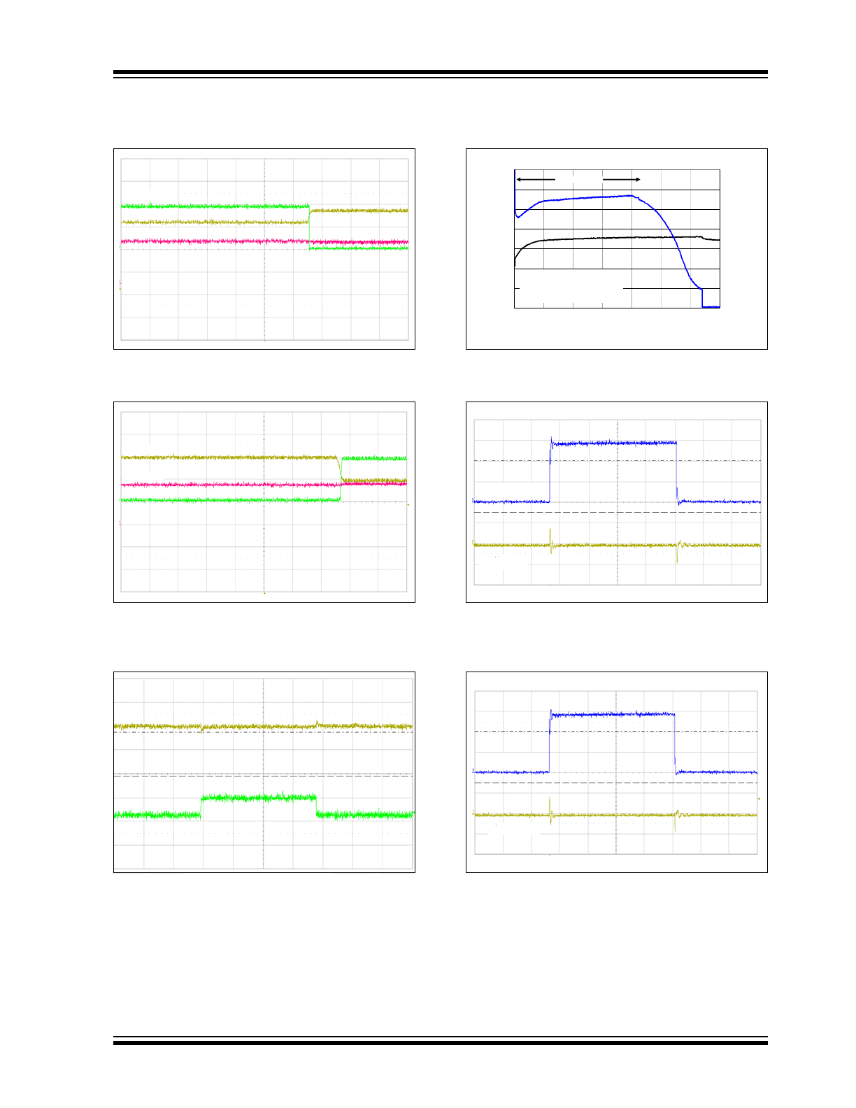
FIGURE 2-13:
Overvoltage Protection Start
(50 ms/Div).
FIGURE 2-14:
Overvoltage Protection Stop
(50 ms/Div).
FIGURE 2-15:
Load Transient Response
(I
LOAD
= 50 mA, Output Ripple: 100 mV/Div,
Output Current: 50 mA/Div, Time: 100 µs/Div).
FIGURE 2-16:
Complete Charge Cycle
(1100 mAh LiFePO
4
Battery).
FIGURE 2-17:
Line Transient Response
(I
LOAD
= 10 mA, Source Voltage: 2V/Div, Output
Ripple: 100 mV/Div, Time: 100 µs/Div).
FIGURE 2-18:
Line Transient Response
(I
LOAD
= 100 mA, Source Voltage: 2V/Div, Output
Ripple: 100 mV/Div, Time: 100 µs/Div).
Charge Current
Input Voltage
Battery Voltage
Charge Current
Input Voltage
Battery Voltage
Output Ripple (mV)
Output Current (mA)
0.0
1.0
2.0
3.0
4.0
5.0
6.0
7.0
0
10
20
30
40
50
60
70
Time (Minutes)
B
a
tt
ery Vo
lt
a
g
e
(
V
)
0
0.1
0.2
0.3
0.4
0.5
0.6
0.7
0.8
0.9
1
S
uppl
y
Cu
rr
e
n
t (
A
)
V
DD
= 5V
R
PROG
= 1 kΩ
1100 mAh LiFePO
4
Battery
Thermal Regulation
Source Voltage (V)
Output Ripple (mV)
Source Voltage (V)
Output Ripple (mV)
MCP73123/223
DS22191E-page 10
2009-2013 Microchip Technology Inc.
3.0
PIN DESCRIPTION
The descriptions of the pins are listed in
Table 3-1
.
TABLE 3-1:
PIN FUNCTION TABLE
3.1
Battery Management Input Supply
(V
DD
)
A supply voltage of [V
REG
(Typical) + 0.3V] to 6.0V is
recommended for MCP73123, while a supply voltage
of [V
REG
(Typical) + 0.3V] to 12.0V is recommended for
MCP73223. Bypass to V
SS
with a minimum of 1 µF.
The V
DD
pin is rated 18V absolute maximum to prevent
sudden rise of input voltage from spikes or low cost
AC-DC wall adapter.
3.2
Battery Charge Control Output
(V
BAT
)
Connect to the positive terminal of the battery. Bypass
to V
SS
with a minimum of 1 µF to ensure loop stability
when the battery is disconnected. The MCP73123 is
designed to provide 3.6V battery regulation voltage for
LiFePO
4
batteries. Undercharge may occur if a typical
Li-Ion or Li-Poly battery is used.
3.3
No Connect (NC)
No connect.
3.4
Status Output (STAT)
STAT is an open-drain logic output for connection to an
LED for charge status indication in stand-alone
applications. Alternatively, a pull-up resistor can be
applied for interfacing to a host microcontroller. Refer to
Table 5-1
for a summary of the status output during a
charge cycle.
3.5
Battery Management 0V Reference
(V
SS
)
Connect to the negative terminal of the battery and
input supply.
3.6
Current Regulation Set (PROG)
The fast charge current is set by placing a resistor from
PROG to V
SS
during constant current (CC) mode.
The PROG pin also serves as a charge control enable
pin. Allowing the PROG pin to float or connecting the
pin to an impedance greater than 200 k
will disable
the MCP73123/223 charger. Refer to
Section 5.5,
"Constant Current Mode – Fast Charge"
, for details.
3.7
Exposed Pad (EP)
The Exposed Thermal Pad (EP) shall be connected to
the exposed copper area on the Printed Circuit Board
(PCB) to enhance thermal power dissipation.
Additional vias on the copper area under the
MCP73123/223 device will improve the performance of
heat dissipation and simplify the assembly process.
Connecting EP to V
SS
is recommended.
MCP73123/223
Symbol
I/O
Description
DFN-10
1, 2
V
DD
I
Battery Management Input Supply
3, 4
V
BAT
I/O
Battery Charge Control Output
5, 6
NC
—
No Connection
7
STAT
O
Battery Charge Status Output
8, 9
V
SS
—
Battery Management 0V Reference
10
PROG
I/O
Battery Charge Current Regulation Program and Charge Control Enable
11
EP
—
Exposed Pad