
2011 Microchip Technology Inc.
DS22288A-page 1
MCP2210
Features:
Universal Serial Bus (USB)
• Supports Full-Speed USB (12 Mb/s)
• Human Interface Device (HID) device
• 128-Byte Buffer to Handle Data Throughput:
- 64-byte transmit
- 64-byte receive
• Fully Configurable VID, PID Assignments and
String Descriptor (factory programming also avail-
able)
• Bus Powered (factory default) or Self-Powered
(can be selected through special USB
commands)
• USB 2.0 Compliant
USB Driver and Software Support
• Uses Standard HID Drivers (built-in support on
Windows
®
XP, Vista, 7, Linux and Mac OS
®
)
• Configuration Utility for Device’s Power-up
Configuration
• Utility for USB-SPI Communication, GPIO
Manipulation and Miscellaneous Features Usage
SPI Master Peripheral
• Supports all Four SPI modes (Mode 0, 1, 2, 3)
• Bit Rates from 1500 bps up to 12 Mbps
• Configurable Delays for SPI Transactions:
- Chip Select (assert) to 1
st
byte of data delay
- Data to data delay
- Data to Chip Select (de-assert) delay
• SPI Transactions Lengths of up to 65535 Bytes
Long
• Up to 9 Chip Select lines – to be used in any
combination for a given SPI transaction (the Chip
Select lines are shared between GPIOs and
alternate function pins; certain GPs – up to 9 of
them – can be assigned with the Chip Select
functionality)
General Purpose Input/Output (GPIO) Pins
• Nine General Purpose I/O Pins
EEPROM
• 256 Bytes of User EEPROM (accessible through
certain USB commands)
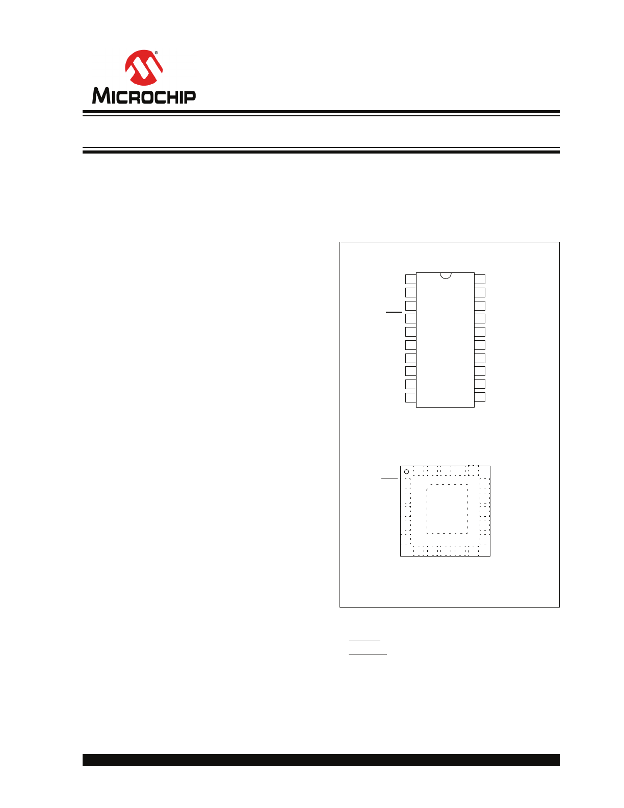
Package Types:
The device will be offered in the following packages:
• 20-lead QFN (5 x 5 mm)
• 20-lead SOIC
• 20-lead SSOP
Other
• USB Activity LED Output
• SSPND Output Pin (to signal USB Suspend state)
• USBCFG Output Pin (indicates when the
enumeration is completed)
• Operating Voltage: 3.3-5.5V
• Oscillator Input: 12 MHz
• Industrial Operating Temperature: -40°C to +85°C
2
MCP2210
SOIC, SSOP
OSC2
OSC1
RST
1
2
3
4
20
19
18
17
V
DD
V
SS
D+
D-
V
USB
GP0 5
16 GP8
GP1 6
15
GP2 7
14 GP6
GP7
MCP2210
5x5 QFN*
GP1
GP2
RST
D-
V
USB
MO
SI
GP8
GP
4
SC
K
GP
5
GP7
OS
C2
OS
C1
V
DD
V
SS
GP0
EP
20
1
19 18 17
3
4
15
14
13
12
6
7
8
9
21
13
12
11
MISO
GP5
SCK
GP3 8
MOSI 9
GP4 10
D+
16
GP3
GP6
5
11
MI
SO
10
* Includes Exposed Thermal Pad (EP); see
Table 1-1
.
USB-to-SPI Protocol Converter with GPIO (Master Mode)
MCP2210
DS22288A-page 2
2011 Microchip Technology Inc.
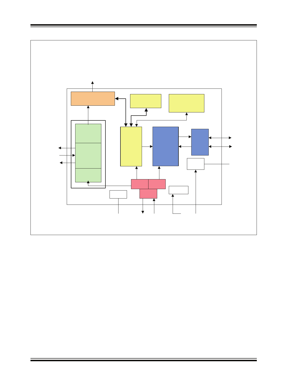
Block Diagram
GPIO
Control
USB
Protocol
Controller
USB
XCVR
V
SS
OSC
State
Clock
USB
Clock
Reset
3.3V
LDO
256-Byte
EEPROM
Configuration
and Control
Regs
SPI
(Master)
Baud
Generator
Chip
Select
Control
GP8-GP0
D+
D-
V
USB
V
DD
RST
OSC1
OSC2
Vss
MOSI
MISO
SCK
CS8:0
Dedicated
function pins

2011 Microchip Technology Inc.
DS22288A-page 3
MCP2210
1.0
FUNCTIONAL DESCRIPTION
The MCP2210 device is a USB-to-SPI Master
converter which enables USB connectivity in
applications that have an SPI interface. The device
reduces external components by integrating the USB
termination resistors.
The MCP2210 also has 256 bytes of integrated user
EEPROM.
The MCP2210 has nine general purpose input/output
pins. Seven pins have alternate functions to indicate
USB and communication status. See
Table 1-1
and
Section 1.6 “GP Module”
for details about the pin
functions.
TABLE 1-1:
PINOUT DESCRIPTION
MCP2210
Symbol
Type
S
tan
dard Func
tion
(GPIO)
Al
ternat
e Fu
nctio
n
1
(Chip
Sele
ct
s)
Al
ternat
e Fu
nctio
n
2
(de
d
ic
ated
func
tions
)
Description
QFN
SOIC,
SSOP
1
4
RST
I
—
—
—
Reset input
2
5
GP0
I/O
GPIO0
CS0
—
General Purpose I/O
3
6
GP1
I/O
GPIO1
CS1
—
General Purpose I/O
4
7
GP2
I/O
GPIO2
CS2
USB Suspend
General Purpose I/O
5
8
GP3
I/O
GPIO3
CS3
SPI Transfer Traffic LED General Purpose I/O
6
9
MOSI
O
—
—
—
SPI Master output
7
10
GP4
I/O
GPIO4
CS4
USB Low Power
General Purpose I/O
8
11
SCK
O
—
—
—
SPI Clock output
9
12
GP5
I/O
GPIO5
CS5
USB Configured
General Purpose I/O
10
13
MISO
I
—
—
—
SPI Master input
11
14
GP6
I/O
GPIO6
CS6
External Interrupt
General Purpose I/O
12
15
GP7
I/O
GPIO7
CS7
SPI Bus Release ACK
General Purpose I/O
13
16
GP8
I/O
GPIO8
CS8
SPI Bus Release REQ
General Purpose I/O
14
17
V
USB
USB
—
—
—
USB Regulator output
15
18
D-
USB
—
—
—
USB D-
16
19
D+
USB
—
—
—
USB D+
17
20
V
SS
GND
—
—
—
Ground
18
1
V
DD
P
—
—
—
Power
19
2
OSC1
I
—
—
—
Oscillator input
20
3
OSC2
O
—
—
—
Oscillator output

MCP2210
DS22288A-page 4
2011 Microchip Technology Inc.
1.1
Supported Operating Systems
The following operating systems are supported:
• Windows XP/Vista/7
• Linux
• Mac OS
1.1.1
ENUMERATION
The MCP2210 will enumerate as a USB device after
Power-on Reset (POR). The device enumerates as a
Human Interface Device (HID) only.
1.1.1.1
Human Interface Device (HID)
The MCP2210 enumerates as an HID, so the device
can be configured and all the other functionalities can
be controlled. A DLL package that facilitates I/O control
through a custom interface is supplied by Microchip
and is available on the product landing page.
1.2
Control Module
The control module is the heart of the MCP2210. All
other modules are tied together and controlled via the
control module. The control module manages the data
transfers between the USB and the SPI, as well as
command requests generated by the USB host
controller, and commands for controlling the function of
the SPI and I/O.
1.2.1
SPI INTERFACE
The control module interfaces to the SPI and USB
modules.
1.2.2
INTERFACING TO THE DEVICE
The MCP2210 can be accessed for reading and writing
via USB host commands. The device cannot be
accessed and controlled via the SPI interface.
1.3
SPI Module
The MCP2210 SPI module provides the MOSI, MISO
and SCK signals to the outside world. The module has
the ability to control the GP pins (as Chip Select) only if
these pins are configured for Chip Select operation.
1.3.1
SPI MODULE FEATURES
The SPI module has the following configurable
features:
• Bit rates
• Delays
• Chip Select pin assignments (up to 9 Chip Select
lines)
All the above features are available for customization
using certain USB commands.
1.3.2
SPI MODULE POWER-UP
CONFIGURATION
Default parameters:
• 1 Mbit
• 4 bytes to transfer per SPI transaction
• GP1 as Chip Select line
1.4
USB Protocol Controller
The USB controller in the MCP2210 is full-speed USB
2.0 compliant.
• HID only device used for:
- SPI transfers
- I/O control
- EEPROM access
- Chip configuration manipulation
• 128-byte buffer to handle data for SPI transfers
- 64-byte transmit
- 64-byte receive
• Fully configurable VID, PID assignments, string
descriptors (stored on-chip) and chip power-up
settings (default chip settings and SPI transfer
parameters)
• Bus powered or self-powered
1.4.1
DESCRIPTORS
The string descriptors are stored internally in the
MCP2210 and they can be changed so when the chip
enumerates, the host gets the customer’s own product
and manufacturer names. They can be customized to
the user’s needs by using the Microchip provided con-
figuration utility or a custom built application that will
send the proper USB commands for storing the new
descriptors into the chip.
1.4.2
USB EVENTS
The MCP2210 provides support for signaling important
USB-related events such as:
• USB Suspend and Resume – these states are
signaled on the GP2, if the pin is configured for its
dedicated function
- USB Suspend mode is entered when a
suspend signaling event is detected on the
USB bus
- USB Resume is signaled when one of the
following events is occurring:
a) Resume signaling is detected or generated
b) A USB Reset signal is detected
c)
A device Reset occurs
• USB device enumerated successfully (this state is
signaled if the GP4 is configured for its dedicated
function)
• USB Low-Power mode
2011 Microchip Technology Inc.
DS22288A-page 5
MCP2210
1.5
USB Transceiver
The MCP2210 has a built-in, USB 2.0, full-speed
transceiver internally connected to the USB module.
The USB transceiver obtains power from the V
USB
pin,
which is internally connected to a 3.3V internal
regulator. The best electrical signal quality is obtained
when V
USB
is locally bypassed with a high-quality
ceramic capacitor.
The internal 3.3V regulator draws power from the V
DD
pin. In certain scenarios, where V
DD
is lower than
3.3V+ internal LDO dropout, the V
USB
pin must be tied
to an external regulated 3.3V. This will allow the USB
transceiver to work correctly, while the I/O voltage in
the rest of the system can be lower than 3.3V. As an
example, in a system where the MCP2210 is used and
the I/O required is of 2.2V, the V
DD
of the chip will be
tied to the 2.2V digital power rail, while the V
USB
pin
must be connected to a regulated 3.3V power supply.
1.5.1
INTERNAL PULL-UP RESISTORS
The MCP2210 device has built-in pull-up resistors
designed to meet the requirements for full-speed USB.
1.5.2
MCP2210 POWER OPTIONS
The following are the main power options for the
MCP2210:
• USB Bus Powered (5V)
• Self Powered (from 3.3V to 5V), while the V
USB
pin is supplied with 3.3V (regulated). If the V
DD
is
powered with 5V, then the V
USB
will be powered
by the internal regulator and the V
USB
pin will
need only a decoupling capacitor
1.5.2.1
Internal Power Supply Details
MCP2210 offers various options for power supply. To
meet the required USB signaling levels, MCP2210
device incorporates an internal LDO used solely by the
USB transceiver, in order to present the correct D+/D
voltage levels.
Figure 1-1
shows the internal connections of the USB
transceiver LDO in relation with the V
DD
power supply
rail. The output of the USB transceiver LDO is tied to
the V
USB
line.
A capacitor connected to the V
USB
pin is required if the
USB transceiver LDO provides the 3.3V supply to the
transceiver.
FIGURE 1-1:
MCP2210 INTERNAL
POWER SUPPLY DETAILS
The provided V
DD
voltage has a direct influence on the
voltage levels present on the GPIO and SPI module
pins (GP8-GP0, MOSI, MISO and SCK). When V
DD
is
5V, all of these pins will have a logical ‘1’ around 5V
with the variations specified in
Section 4.1 “DC Char-
acteristics”
.
For applications that require a 3.3V logical ‘1’ level,
V
DD
must be connected to a power supply providing
the 3.3V voltage. In this case, the internal USB
transceiver LDO cannot provide the required 3.3V
power. It is necessary to also connect the V
USB
pin of
the MCP2210 to the 3.3V power supply rail. This way,
the USB transceiver is powered up directly from the
3.3V power supply.
1.5.2.2
USB Bus Powered (5V)
In Bus Power Only mode, the entire power for the
application is drawn from the USB (see
Figure 1-2
).
This is effectively the simplest power method for the
device.
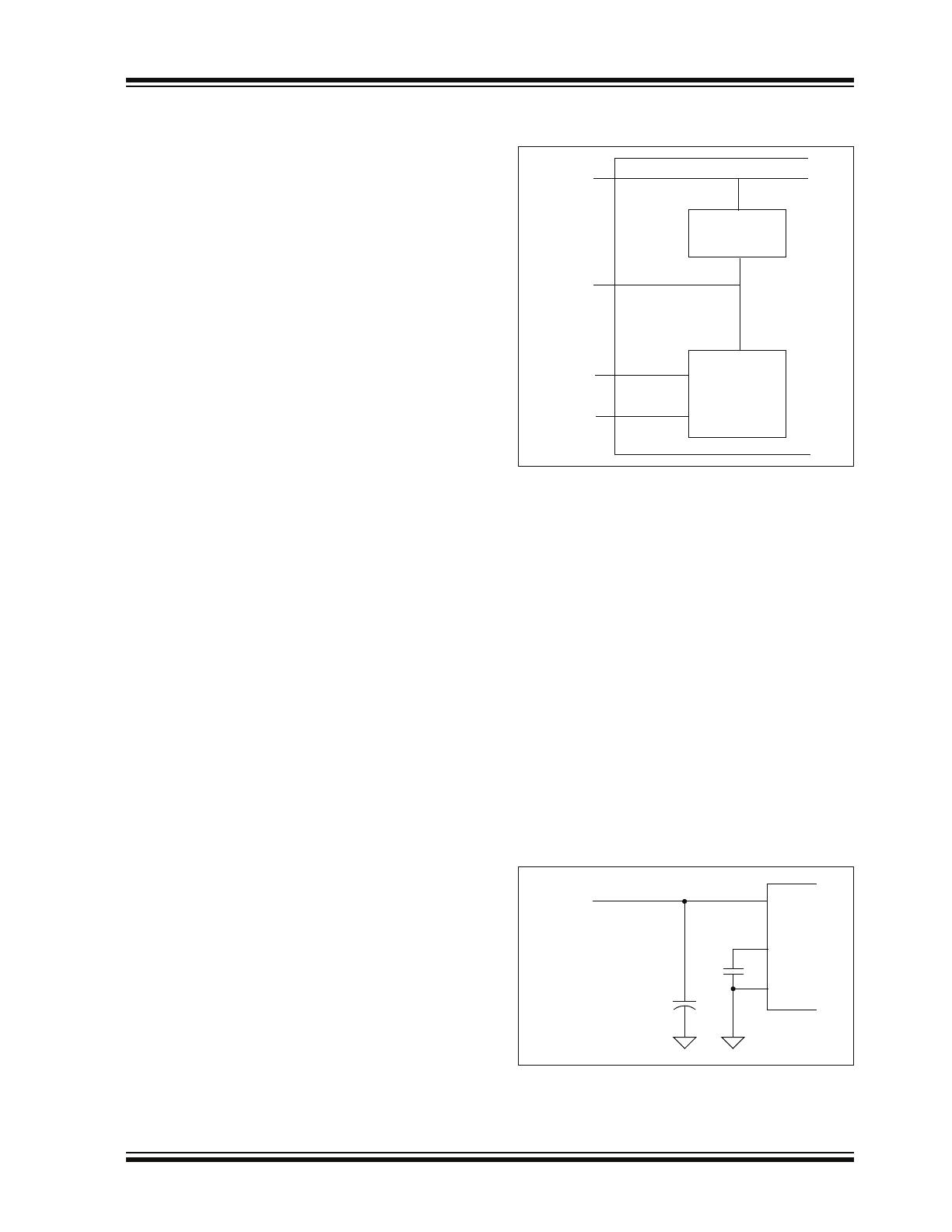
FIGURE 1-2:
BUS POWER ONLY
LDO
3.3V
USB
Transceiver
D+
V
DD
V
USB
D-
IN
OUT
V
DD
V
USB
V
SS
V
BUS
MCP2210
DS22288A-page 6
2011 Microchip Technology Inc.
In order to meet the inrush current requirements of the
USB 2.0 specifications, the total effective capacitance
appearing across V
BUS
and ground must be no more
than 10 µF.
If it is more than 10 µF, some kind of inrush
limiting is required. For more details on Inrush Current
Limiting, see the current Universal Serial Bus Specifi-
cation.
According to the USB 2.0 specification, all USB devices
must also support a Low-Power Suspend mode. In the
USB Suspend mode, devices must consume no more
than 500 µA (or 2.5 mA for high powered devices that
are remote wake-up capable) from the 5V V
BUS
line of
the USB cable.
The host signals the USB device to enter Suspend
mode by stopping all USB traffic to that device for more
than 3 ms.
The USB bus provides a 5V voltage. However, the USB
transceiver requires 3.3V for the signaling (on D+ and
D- lines).
During USB Suspend mode, the D+ or D- pull-up resis-
tor must remain active, which will consume some of the
allowed suspend current budget (500 µA/2.5 mA).
The V
USB
pin is required to have an external bypass
capacitor. It is recommended that the capacitor be a
ceramic cap, between 0.22 and 0.47 µF.
Figure 1-3
shows a circuit where the MCP2210 internal
LDO is used to provide 3.3V to the USB transceiver.
The voltage on the V
DD
affects the voltage levels onto
the GP and SPI module pins (GP8-GP0, MOSI, MISO
and SCK). With V
DD
at 5V, these pins will have a logic
‘1’ of 5V with the variations specified in
Section 4.1
“DC Characteristics”
.
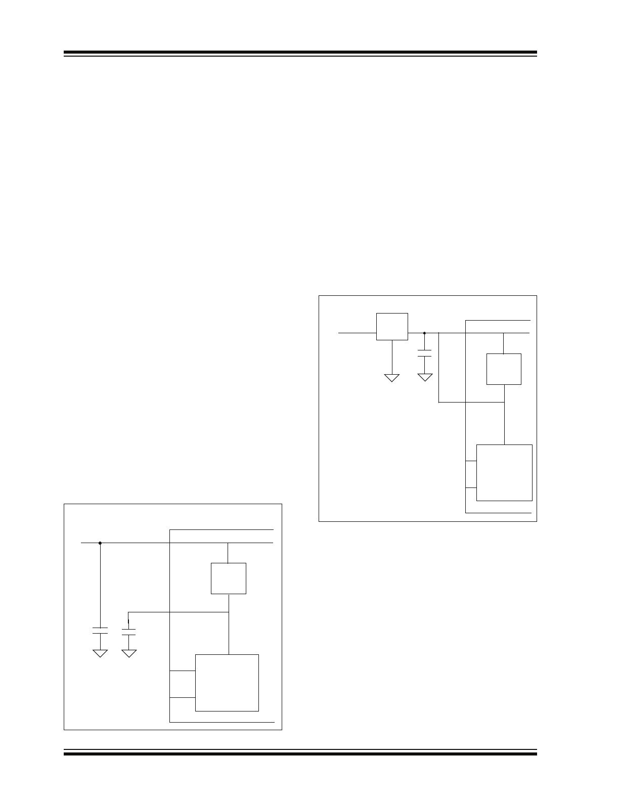
FIGURE 1-3:
TYPICAL POWER SUPPLY
OPTION USING THE 5V
PROVIDED BY THE USB
1.5.2.3
3.3V – Self Powered
Typically, many embedded applications are using 3.3V
or lower power supplies. When such an option is avail-
able in the target system, MCP2210 can be powered
up (V
DD
) from the existing power supply rail. The typi-
cal connections for MCP2210 powered from 3.3V rail
are shown in
Figure 1-4
.
In this example MCP2210 has both V
DD
and V
USB
lines
tied to the 3.3V rail. These tied connections disable the
internal USB transceiver LDO of the MCP2210 to
regulate the power supply on V
USB
pin. Another
consequence is that the ‘1’ logical level on the GP and
SPI pins will be at the 3.3V level, in accordance with the
variations specified in
Section 4.1 “DC
Characteristics”
.
FIGURE 1-4:
USING AN EXTERNALLY
PROVIDED 3.3V POWER
SUPPLY
LDO
3.3V
USB
Transceiver
D+
V
DD
V
USB
D-
IN
OUT
5V (USB Bus)
or external
power supply
LDO
3.3V
D+
V
DD
V
USB
D-
IN
OUT
5V (USB Bus)
or external
power supply
External
USB
Transceiver
3.3V
LDO

2011 Microchip Technology Inc.
DS22288A-page 7
MCP2210
1.6
GP Module
The GP module features nine I/O lines.
1.6.1
CONFIGURABLE PIN FUNCTIONS
The pins can be configured as:
• GPIO – individually configurable, general purpose
input or output
• Chip Select pins – used by the SPI module
• Alternate function pins – used for miscellaneous
features such as:
- SSPND – USB Suspend and Resume states
- USBCFG – indicates USB configuration
status
- LOWPWR – signals when the host does not
accept the requirements (presented during
enumeration) and the chip is not configured.
In this mode, the whole system powered from
the USB host should draw up to 100 mA.
- External Interrupt Input – used to count
external events
- SPI bus Release Request – used to request
SPI bus access from the MCP2210
- SPI bus Release Acknowledge – used to
acknowledge when the MCP2210 has
released the SPI bus
- LED – indicates SPI traffic led
1.6.1.1
GPIO Pins Function
The GP pins (if enabled for GPIO functionality) can be
used as digital inputs/outputs.
These pins can be read (both inputs and outputs) and
written (only the outputs).
1.6.1.2
Chip Select Pins Function
The GP pins (if enabled for the Chip Select functional-
ity) are controlled by the SPI module. Their Idle/Active
value is determined by the SPI transfer parameters.
1.6.1.3
SSPND Pin Function
The GP2 pin (if enabled for this functionality) reflects
the USB state (Suspend/Resume). The pin is active
‘low’ when the Suspend state has been issued by the
USB host.
Likewise, the pin drives ‘high’ after the Resume state is
achieved.
This pin allows the application to go into Low-Power
mode when USB communication is suspended, and
switches to a full active state when USB activity is
resumed.
1.6.1.4
USBCFG Pin Function
The GP5 pin (if enabled for this functionality) starts out
‘high’ during power-up or after Reset, and goes ‘low’
after the device successfully configures to the USB.
The pin will go ‘high’ when in Suspend mode and ‘low’
when the USB resumes.
1.6.1.5
LOWPWR Pin Function
The GP4 pin (if enabled for this functionality) starts out
‘low’ during power-up or after Reset, and goes ‘high’
after the device successfully configures to the USB.
The pin will go ‘low’ when in Suspend mode and ‘high’
when the USB resumes.
1.6.1.6
External Interrupt Input Pin Function
The GP4 pin (if enabled for this functionality) is used as
an interrupt input pin and it will count interrupt events
such as:
• Falling edges
• Rising edges
• Low-logic pulses
• High-logic pulses
1.6.1.7
SPI Bus Release Request Pin
Function
The GP8 pin (if enabled for this functionality) is used by
an external device to request the MCP2210 to release
the SPI bus. This way, more than one SPI master can
have access to the SPI slave chips on the bus. When
this pin is driven ‘low’, the MCP2210 will examine the
request and, based on the conditions and internal logic,
it might release the SPI bus. If there is an ongoing SPI
transfer taking place at the moment when an external
device requests the bus, MCP2210 will release it after
the transfer is completed or if the USB host cancels the
current SPI transfer.
1.6.1.8
SPI Bus Release Acknowledge Pin
Function
The GP7 pin (if enabled for this functionality) is used by
the MCP2210 to signal back if the SPI bus was
released. When a SPI bus release request is registered
by the MCP2210, based on the condition and internal
logic, the chip might release the bus. The bus is
released immediately if there is no SPI transfer taking
place, or it will do so after the current SPI transfer is
finished or cancelled by the USB host.
1.6.1.9
LED Pin Function
The GP3 pin (if enabled for this functionality) is used as
an SPI traffic indication. When an SPI transfer is taking
place (active state for this pin), this pin will be driven
‘low’. When there is no SPI traffic taking place, the pin
is in its inactive state or logic ‘high’.
MCP2210
DS22288A-page 8
2011 Microchip Technology Inc.
1.7
EEPROM Module
The EEPROM module is a 256-byte array of nonvola-
tile memory. The memory locations are accessed for
read/write operations solely via USB host commands.
The memory cells for data EEPROM are rated to
endure thousands of erase/write cycles, up to 100K for
EEPROM.
Data retention without refresh is conservatively
estimated to be greater than 40 years.
1.8
Reset/POR
1.8.1
RESET PIN
The RST pin provides a method for triggering an
external Reset of the device. A Reset is generated by
holding the pin low. MCP2210 has a noise filter in the
Reset path which detects and ignores small pulses.
1.8.2
POR
A POR pulse is generated on-chip whenever V
DD
rises
above a certain threshold. This allows the device to
start in the initialized state when V
DD
is adequate for
operation.
To take advantage of the POR circuitry, tie the RST pin
through a resistor (1 k
to 10 k) to V
DD
. This will
eliminate external RC components usually needed to
create a POR delay.
When the device starts normal operation (i.e., exits the
Reset condition), the device operating parameters
(voltage, frequency, temperature, etc.) must be met to
ensure operation. If these conditions are not achieved,
the device must be held in Reset until the operating
conditions are met.
1.9
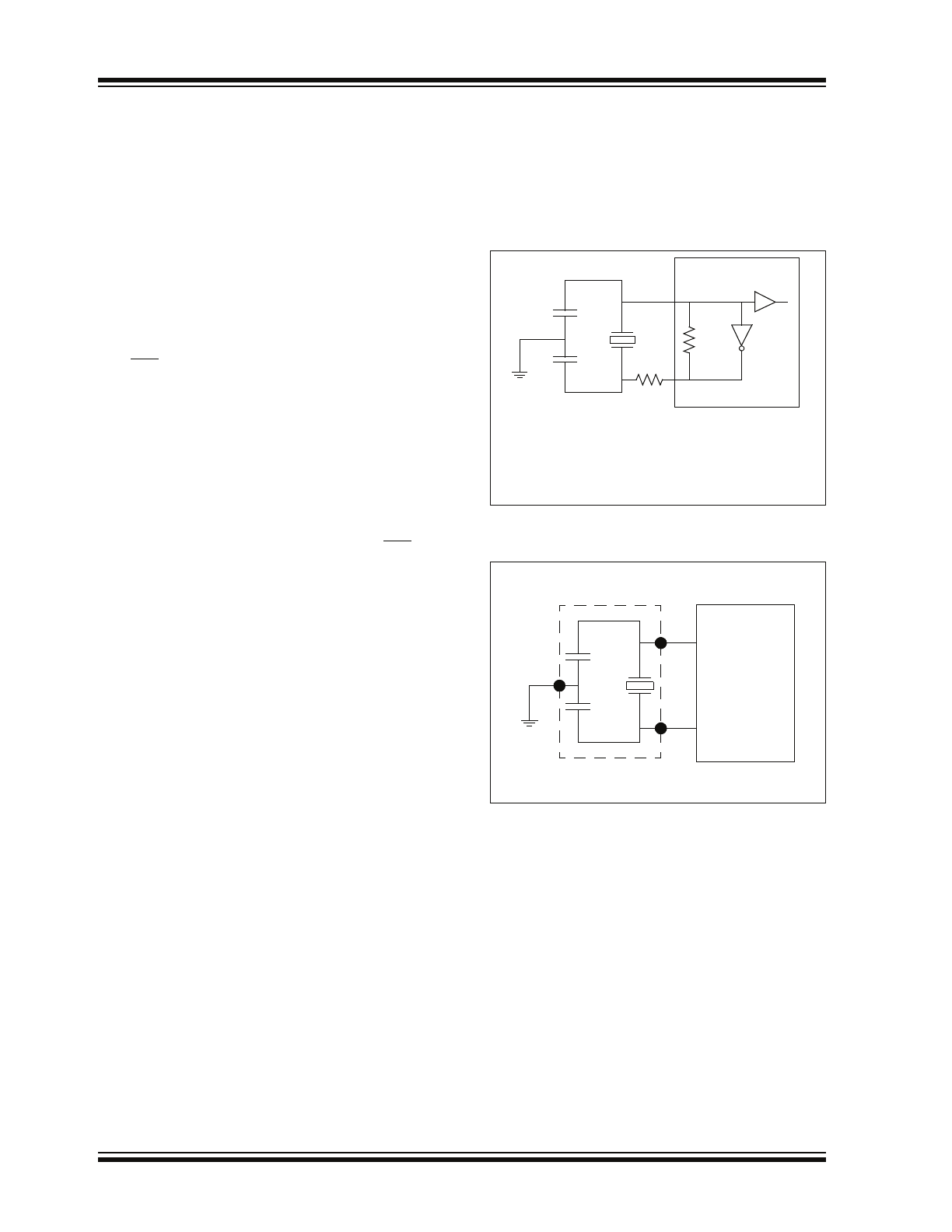
Oscillator
The input clock must be 12 MHz to provide the proper
frequency for the USB module. USB full-speed is
nominally 12 Mb/s. The clock input accuracy is ±0.25%
(2,500 ppm maximum).
FIGURE 1-5:
QUARTZ CRYSTAL
OPERATION
FIGURE 1-6:
CERAMIC RESONATOR
OPERATION
Quartz Crystal
12 MHz
OSC1
OSC2
R
S
(
1
)
R
F
(
2
)
MCP2210
Note 1: A series resistor (R
S
) may be required for
quartz crystals with high drive level.
2: The value of R
F
is typically between 2 M
to
10 M
..
Example: muRata
®
CSTCE12M0G15L
OSC1
OSC2
Resonator
12 MHz
MCP2210

2011 Microchip Technology Inc.
DS22288A-page 9
MCP2210
2.0
MCP2210 FUNCTIONAL
DESCRIPTION
The MCP2210 uses NVRAM to store relevant chip
settings. These settings are loaded by the chip during
the power-up process and they are used for GP
designation and SPI transfers.
The NVRAM settings at power-up (or Reset) are
loaded into the RAM portion of the chip and they can be
altered through certain USB commands. This is very
useful since it allows dynamic reconfiguring of the GPs
or SPI transfer parameters. A practical example to
illustrate this mechanism is a system which uses at
least two SPI slave chips and the GPs in the MCP2210
for various GPIO purposes. The default SPI settings
might be ok for one of the SPI slave chips, but not for
the 2
nd
. At first, the PC application will make an SPI
transfer to the first
chip, using the NVRAM copy of the
SPI settings. Then, by sending a certain USB
command, the SPI transfer settings residing in RAM
will be altered in order to fit the SPI transfer
requirements of the second chip.
Also, if the altered SPI transfer settings are needed to
be the default power-up (or Reset) settings for SPI, the
user can send a series of USB commands in order to
store the current (RAM) SPI settings into NVRAM. In
this way, these new settings will be the power-up
default SPI settings.
The NVRAM settings and EEPROM contents can be
protected by password access means, or they can be
permanently locked without any possible further
modification.
2.1
MCP2210 NVRAM Settings
The chip settings that can be stored in the NVRAM
area are as follows:
• SPI transfer parameters:
- SPI bit rate
- SPI mode
- Idle Chip Select values
- Active Chip Select values
- SPI transfer configurable delays
- Number of bytes to read/write for the given
SPI transfer
• GP designation:
- GPIO
- Chip Select
- Dedicated function
• GPIO default direction (applies only to those GPs
designated as GPIOs)
• GPIO default output value (applies only to those
GPs designated as output GPIOs)
• Chip mode flags:
- Remote wake-up capability
- External Interrupt Pin mode (applies only
when GP6 is designated for this function)
- SPI bus release enable/disable – enable/
disable the release of the SPI bus when there
is no SPI transfer (useful when more than
one SPI master on the bus)
• NVRAM Access mode:
- Full access (no protection – factory default)
- Password protection
- Permanently locked
• Password (relevant when password protection
mechanism is
active)
The specified settings are loaded at power-up or Reset
moments, and they can be altered through certain USB
commands.
When a NVRAM conditional access method is already
in place, such as password protection, the NVRAM
settings modification is permitted only when the user
has supplied the correct password for the chip. The
RAM settings can be altered even when a password
protection or permanent lock mechanism are in place.
This allows the user to communicate with various SPI
slave chips without knowing the password, but it will not
allow the modification of the power-up default settings
in NVRAM.
2.2
SPI Transfers
The MCP2210 device provides advanced SPI
communication features such as configurable delays
and multiple
Chip Select support.
The configurable delays are related to certain aspects
of the SPI transfer:
• The delay between the assertion of Chip Select(s)
and the first data byte (
Figure 2-1
)
FIGURE 2-1:
CHIP SELECT TO DATA
DELAY
T
CS2DATA
CS
SCK
MOSI
MISO
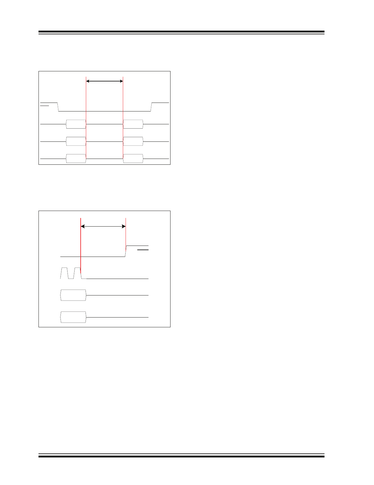
MCP2210
DS22288A-page 10
2011 Microchip Technology Inc.
• The delay between subsequent data bytes
(
Figure 2-2
)
FIGURE 2-2:
DATA-TO-DATA DELAY
• The delay between the end of the last byte (of the
SPI transfer) and the de-assertion of the Chip
Select(s)
FIGURE 2-3:
DATA TO CHIP SELECT
DELAY
For a particular SPI transfer, the user can choose any
number (out of the available ones) of Chip Select pins.
The SPI transfer parameters contain two fields where
the user will specify the Chip Select values when the
SPI transfer is active/idle. This mechanism allows the
user to specify any combination of Chip Select values
for the Idle mode and some other combination for the
Active mode (SPI transfer active).
T
DATA2DATA
CS
SCK
MOSI
MISO
T
DATA2CS
CS
SCK
MOSI
MISO