

1
FDC37B78x
Super I/O Controller with ACPI Support,
Real Time Clock and Consumer IR
FEATURES
5 Volt Operation
PC98/99 and ACPI 1.0 Compliant
Battery Back-up for Wake-Events
ISA Plug-and-Play Compatible Register Set
-
12 IRQ Options
-
15 Serial IRQ Options
-
16 Bit Address Qualification
-
Four DMA Options
-
12mA AT Bus Drivers
BIOS
Buffer
20 GPI/O Pins
32KHz Standby Clock Output
Soft Power Management
ACPI/PME
Support
SCI/SMI
Support
- Watchdog
timer
-
Power Button Override Event
-
Either Edge Triggered Interrupts
Intelligent Auto Power Management
-
Shadowed Write-only Registers
-
Programmable Wake-up Event Interface
8042 Keyboard Controller
-
2K Program ROM
-
256 Bytes Data RAM
-
Asynchronous Access to Two Data
Registers and One Status Register
-
Supports Interrupt and Polling Access
-
8 Bit Timer/Counter
-
Port 92 Support
-
Fast Gate A20 and Hardware Keyboard
Reset
Real Time Clock
-
Day of Month Alarm, Century Byte
-
MC146818 and DS1287 Compatible
-
256 Bytes of Battery Backed CMOS in
Two Banks of 128 Bytes
-
128 Bytes of CMOS RAM Lockable in
4x32 Byte Blocks
-
12 and 24 Hour Time Format
-
Binary and BCD Format
-
5
μA Standby Battery Current (max)
1
2.88MB Super I/O Floppy Disk Controller
-
Relocatable to 480 Different Addresses
-
Licensed CMOS 765B Floppy Disk
Controller
-
Advanced Digital Data Separator
-
SMSC's Proprietary 82077AA
Compatible Core
-
Sophisticated Power Control Circuitry
(PCC) Including Multiple Powerdown
Modes for Reduced Power
Consumption
-
Supports Two Floppy Drives Directly
-
Software Write Protect
-
FDC on Parallel Port
-
Low Power CMOS Design
-
Supports Vertical Recording Format
-
16 Byte Data FIFO
-
100% IBM Compatibility
-
Detects All Overrun and Underrun
Conditions
-
24mA Drivers and Schmitt Trigger
Inputs
Enhanced FDC Digital Data Separator
-
Low Cost Implementation
-
No Filter Components Required
-
2 Mbps, 1 Mbps, 500 Kbps, 300 Kbps,
250 Kbps Data Rates
- Programmable
Precompensation
Modes

2
Serial
Ports
-
Relocatable to 480 Different Addresses
-
Two High Speed NS16C550 Compatible
-
UARTs with Send/Receive 16 Byte
FIFOs
-
Programmable Baud Rate Generator
-
Modem Control Circuitry Including 230K
and 460K Baud
-
IrDA 1.0, Consumer IR, HP-SIR, ASK-
IR Support
-
Ring Wake Filter
Multi-Mode Parallel Port with ChiProtect
-
Relocatable to 480 Different Addresses
- Standard
Mode
-
IBM PC/XT, PC/AT, and PS/2
Compatible Bidirectional ParallelPort
- Enhanced
Mode
-
Enhanced Parallel Port (EPP)
Compatible
-
EPP 1.7 and EPP 1.9 (IEEE 1284
Compliant)
-
High Speed Mode
-
Microsoft and Hewlett Packard
-
Extended Capabilities Port (ECP)
Compatible (IEEE 1284 Compliant)
-
Incorporates ChiProtect Circuitry for
Protection Against Damage Due to
Printer Power-On
-
14 mA Output Drivers
128 Pin QFP package, lead-free RoHS
compliant package also available
Note 1: Please contact SMSC for the latest value.
ORDERING INFORMATION
Order Numbers:
FDC37B787QFP for 128 pin QFP package
FDC37B787-NS for 128 pin QFP lead-free RoHS compliant package

3
TABLE OF CONTENTS
FEATURES ........................................................................................................................................... 1
GENERAL DESCRIPTION ................................................................................................................. 6
DESCRIPTION OF PIN FUNCTIONS............................................................................................... 7
BUFFER TYPE DESCRIPTIONS .................................................................................................... 11
REFERENCE DOCUMENTS ........................................................................................................... 13
FUNCTIONAL DESCRIPTION......................................................................................................... 14
SUPER
I/O
REGISTERS ............................................................................................................... 14
HOST
PROCESSOR
INTERFACE .............................................................................................. 14
FLOPPY DISK CONTROLLER....................................................................................................... 16
FDC INTERNAL REGISTERS ................................................................................................. 16
COMMAND SET/DESCRIPTIONS.......................................................................................... 41
Force Write Protect .................................................................................................................. 70
SERIAL PORT (UART) ..................................................................................................................... 70
REGISTER DESCRIPTION ...................................................................................................... 70
INFRARED INTERFACE .................................................................................................................. 88
PARALLEL PORT ............................................................................................................................. 88
IBM XT/AT COMPATIBLE, BI-DIRECTIONAL AND EPP MODES........................................ 90
EXTENDED CAPABILITIES PARALLEL PORT.......................................................................... 96
PARALLEL
PORT
FLOPPY
DISK
CONTROLLER .................................................................. 108
POWER MANAGEMENT................................................................................................................ 110
FDC Power Management ...................................................................................................... 110
UART Power Management ................................................................................................... 115
Parallel Port.............................................................................................................................. 115
V
BAT
Support ............................................................................................................................ 115
V
TR
Support .............................................................................................................................. 115
Internal PWRGOOD................................................................................................................ 116
CIRCC PLL Power Control ................................................................................................... 116
32.768 kHz Standby Clock Output...................................................................................... 116
BIOS BUFFER.................................................................................................................................. 121
GENERAL PURPOSE I/O .............................................................................................................. 123

4
Description............................................................................................................................... 123
RUN STATE GPIO DATA REGISTER ACCESS................................................................ 123
GPIO OPERATION .................................................................................................................. 127
8042 KEYBOARD CONTROLLER DESCRIPTION ................................................................... 130
RTC INTERFACE............................................................................................................................. 138
SOFT POWER MANAGEMENT .................................................................................................... 148
ACPI/PME/SMI FEATURES........................................................................................................... 152
ACPI Features.......................................................................................................................... 152
Wake Events ............................................................................................................................. 153
PME SUPPORT........................................................................................................................ 154
ACPI/PME/SMI
REGISTERS...................................................................................................... 154
Register Description ................................................................................................................. 154
Wakeup Event Configuration is Retained by Battery Power ...................................... 156
Register Block ......................................................................................................................... 156
ACPI REGISTERS ................................................................................................................... 157
CONFIGURATION ........................................................................................................................... 168
SYSTEM
ELEMENTS .................................................................................................................. 168
Entering the Configuration State........................................................................................ 149
Exiting the Configuration State .......................................................................................... 149
CONFIGURATION SEQUENCE............................................................................................ 149
CONFIGURATION REGISTERS ................................................................................................... 172
Chip Level (Global) Control/Configuration Registers [0x00-0x2F]............................ 176
Logical Device Configuration/Control Registers [0x30-0xFF] .................................... 179
Logical Device Registers...................................................................................................... 179
I/O Base Address Configuration Register........................................................................ 181
Interrupt Select Configuration Register ........................................................................... 183
DMA Channel Select Configuration Register .................................................................. 184
SMSC Defined Logical Device Configuration Registers .............................................. 185
Parallel Port, Logical Device 3 ............................................................................................ 188
Serial Port 1, Logical Device 4 ............................................................................................ 189
Serial Port 2, Logical Device 5 ............................................................................................ 191
RTC, Logical Device 6 ........................................................................................................... 192
KYBD, Logical Device 7 ........................................................................................................ 193
Auxiliary I/O, Logical Device 8 ............................................................................................ 194
ACPI, Logical Device A ......................................................................................................... 212
OPERATIONAL DESCRIPTION ................................................................................................... 218
MAXIMUM
GUARANTEED
RATINGS ...................................................................................... 218
DC
ELECTRICAL
CHARACTERISTICS ................................................................................... 218

5
AC
TIMING
DIAGRAMS .............................................................................................................. 223
CAPACITIVE LOADING ......................................................................................................... 223
IOW Timing Port 92 ................................................................................................................ 224
POWER-UP TIMING................................................................................................................ 225
Button Timing.......................................................................................................................... 226
ROM INTERFACE.................................................................................................................... 227
ISA WRITE ................................................................................................................................ 228
ISA READ.................................................................................................................................. 229
8042 CPU .................................................................................................................................. 231
CLOCK TIMING........................................................................................................................ 232
Burst Transfer DMA Timing ................................................................................................. 235
DISK DRIVE TIMING ............................................................................................................... 237
SERIAL PORT .......................................................................................................................... 238
Parallel Port.............................................................................................................................. 239
EPP 1.9 Data or Address Write Cycle................................................................................ 240
EPP 1.9 Data or Address Read Cycle................................................................................ 242
EPP 1.7 Data Or Address Write Cycle ............................................................................... 244
EPP 1.7 Data or Address Read Cycle................................................................................ 246
ECP PARALLEL PORT TIMING ........................................................................................... 249
Serial Port Infrared Timing ................................................................................................... 254

6
GENERAL DESCRIPTION
The FDC37B78x with advanced Consumer IR
and IrDA v1.0 support incorporates a keyboard
interface, real-time clock, SMSC's true CMOS
765B floppy disk controller, advanced digital data
separator, 16 byte data FIFO, two 16C550
compatible UARTs, one Multi-Mode parallel port
which includes ChiProtect circuitry plus EPP and
ECP support, on-chip 12 mA AT bus drivers, and
two floppy direct drive support, soft power
management and SMI support and Intelligent
Power Management including PME and
SCI/ACPI support. The true CMOS 765B core
provides 100% compatibility with IBM PC/XT and
PC/AT architectures in addition to providing data
overflow and underflow protection. The SMSC
advanced digital data separator incorporates
SMSC's patented data separator technology,
allowing for ease of testing and use. Both on-chip
UARTs are compatible with the NS16C550. The
parallel port, the IDE interface, and the game port
select logic are compatible with IBM PC/AT
architecture, as well as EPP and ECP. The
FDC37B78x incorporates sophisticated power
control circuitry (PCC) which includes support for
keyboard, mouse, modem ring, power button
support and consumer infrared wake-up events.
The PCC supports multiple low power down
modes.
The FDC37B78x provides features for compliance
with the “Advanced Configuration and Power
Interface Specification” (ACPI).
These features include support of both legacy and
ACPI power management models through the
selection of SMI or SCI. It implements a power
button override event (4 second button hold to turn
off the system) and either edge triggered
interrupts.
The FDC37B78x provides support for the ISA
Plug-and-Play Standard (Version 1.0a) and
provides for the recommended functionality to
support Windows '95, PC97 and PC98. Through
internal configuration registers, each of the
FDC37B78x 's logical device's I/O address, DMA
channel and IRQ channel may be programmed.
There are 480 I/O address location options, 12
IRQ options or Serial IRQ option, and four DMA
channel options for each logical device.
The FDC37B78x Floppy Disk Controller and data
separator do not require any external filter
components and are therefore easy to use, offer
lower system cost and reduced board area. The
FDC is software and register compatible with
SMSC's proprietary 82077AA core.
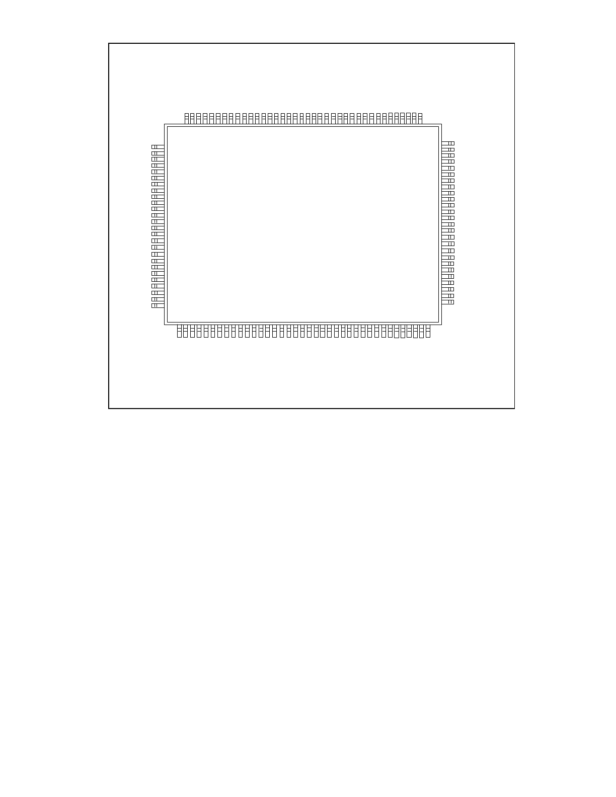
6
FIGURE 1 - FDC37B78x PIN CONFIGURATION
FDC37B78x
128 Pin QFP
PD
0
nS
L
C
T
IN
nI
N
IT
VC
C
n
R
O
M
OE/IR
Q
1
2
/G
P
5
4
/E
ETI
n
R
O
M
CS
/I
RQ
11/
G
P
53/
EE
TI
RD7/
IR
Q
10/
G
P
67
RD6/
IR
Q
8/
G
P
66
RD
5
/I
R
Q
7
/G
P
6
5
R
D
4
/IR
Q
6
/G
P
6
4
/P1
7
R
D
3/
IR
Q
5
/G
P63/
WDT
R
D
2
/IR
Q
4
/G
P6
2
/n
R
IN
G
R
D
1
/IR
Q
3
/G
P6
1
/L
E
D
R
D
0
/IR
Q
1
/G
P6
0
/n
S
M
I
KC
LK
KD
A
T
VT
R
XT
A
L
2
A
VSS
XT
AL1
GP1
5
/I
R
T
X
2
VBA
T
G
P
14
/I
RRX
2
G
P
13/
L
E
D
G
P
1
2
/W
D
T
/P
1
7
/EE
T
I
G
P
11
/n
RI
NG
/E
E
T
I
G
P
10/
n
S
M
I
A2
0M
KBD
R
S
T
VSS
MC
L
K
MD
A
T
PD
6
PD
5
PD
4
PD
3
PD
2
PD
1
102
10
1
100
99
98
97
96
95
94
93
92
91
90
89
88
87
86
85
84
83
82
81
80
79
78
77
76
75
74
73
72
71
70
69
68
67
66
65
64
63
62
61
60
59
58
57
56
55
54
53
52
51
50
49
48
47
46
45
44
43
42
41
40
39
IOCHRDY
TC
VCC
DRQ3
nDACK3
DRQ2
nDACK2
DRQ1
nDACK1
DRQ0
nDACK0
RESET_DRV
SD7
SD6
SD5
SD4
VSS
SD3
SD2
SD1
SD0
AEN
nIOW
nIOR
SER_IRQ/IRQ15
PCI_CLK/IRQ14/GP50
1
2
3
4
5
6
7
8
9
10
11
12
13
14
15
16
17
18
19
20
21
22
23
24
25
26
27
28
29
30
31
32
33
34
35
36
37
38
DR
V
D
E
N
0
D
R
V
D
EN1/
G
P
52/
IR
Q
8
/n
SM
I
nM
T
R
0
nDS1/
G
P
1
7
nDS
0
nM
T
R
1/
G
P
16
VS
S
nDI
R
nST
E
P
nWD
A
T
A
nWG
A
T
E
nHDS
E
L
n
INDE
X
nT
R
K
0
nWR
T
PR
T
nR
D
A
T
A
nDSK
CH
G
C
L
K32O
UT
nP
O
W
ER
O
N
BU
T
T
O
N
_
IN
n
P
M
E
/SC
I/IR
Q
9
CL
O
C
K
I
SA
9
SA0
SA1
SA
2
SA4
SA6
SA7
SA8
SA3
SA5
SA10
SA11
SA12
SA13
SA14
SA15
103
104
105
106
107
108
109
110
111
112
113
114
115
116
117
118
119
120
121
122
123
124
125
126
127
128
nCTS2
nRTS2
nDSR2
TXD2/IRTX
RXD2/IRRX
nDCD2
VCC
nRI2
nDCD1
nRI1
nDTR1
nCTS1
nRTS1/SYSOP
nDSR1
TXD1
RXD1
nSTROBE
nALF
nERROR
nACK
BUSY
PE
SLCT
VSS
PD7
nDTR2
7
DESCRIPTION OF PIN FUNCTIONS
PIN
No./QFP
NAME
TOTAL
SYMBOL
BUFFER TYPE
PROCESSOR/HOST INTERFACE (40)
44-47,
49-52
System Data Bus
8
SD[0:7]
IO12
23-38
16-bit System Address Bus
16
SA[0:15]
I
43 Address
Enable
1 AEN
I
64
I/O Channel Ready
1
IOCHRDY
OD12
53
ISA Reset Drive
1
RESET_DRV
IS
40 Serial
IRQ/IRQ15
1 SER_IRQ
IO12
39 PCI
Clock/IRQ14/GP50
1 PCI_CLK
IO12
55
DMA Request 0
1
DRQ0
O12
57
DMA Request 1
1
DRQ1
O12
59
DMA Request 2
1
DRQ2
O12
61
DMA Request 3
1
DRQ3
O12
54
DMA Acknowledge 0
1
nDACK0
I
56
DMA Acknowledge 1
1
nDACK1
I
58
DMA Acknowledge 2
1
nDACK2
I
60
DMA Acknowledge 3
1
nDACK3
I
63 Terminal
Count
1 TC
I
41 I/O
Read
1 nIOR
I
42 I/O
Write
1 nIOW
I
CLOCKS (4)
22
14.318MHz Clock Input
1
CLOCKI
I
66
32.768kHz Crystal Input
1
XTAL1
ICLK
68
32.768kHz Crystal Driver
1
XTAL2
OCLK
18
32.768kHz Clock Out
1
CLK32OUT
O8
POWER PINS (10)
62, 93,
121
+5V Supply Voltage
3
VCC
8
PIN
No./QFP
NAME
TOTAL
SYMBOL
BUFFER TYPE
7, 48,
74, 104
Digital Ground
4
VSS
67 Analog
Ground
1 AVSS
69
Trickle Supply Voltage
1
VTR
65 Battery
Voltage
1 VBAT
POWER MANAGEMENT (3)
19 Power
On
1 nPOWERON
OD24
20 Button
In
1 BUTTON_IN
I
21
Power Management Event/SCI/IRQ9
1
nPME
O12
FDD INTERFACE (16)
16
Read Disk Data
1
nRDATA
IS
11
Write Gate
1
nWGATE
O24
10
Write Disk Data
1
nWDATA
O24
12 Head
Select
1 nHDSEL
O24
8 Step
Direction
1 nDIR
O24
9 Step
Pulse
1 nSTEP
O24
17 Disk
Change
1 nDSKCHG
IS
5
Drive Select 0
1
nDS0
O24
6
Drive Select 1/GP17
1
nDS1
IO24
3
Motor On 0
1
nMTR0
O24
4
Motor On 1/GP16
1
nMTR1
IO24
15 Write
Protected
1 nWRTPRT
IS
14 Track
0
1 nTRKO
IS
13
Index Pulse Input 1
nINDEX
IS
1
Drive Density Select 0
1
DRVDEN0
O24
2
Drive Density Select 1/GP52/IRQ8/nSMI
1
DRVDEN1
IO24
GENERAL PURPOSE I/O (6)
77 General
Purpose
10/nSMI 1
GP10
IO12
78
General Purpose 11/nRING/EETI
1
GP11
IO4
9
PIN
No./QFP
NAME
TOTAL
SYMBOL
BUFFER TYPE
79
General Purpose 12/WDT/P17/EETI
1
GP12
IO4
80
General Purpose 13/LED Driver
1
GP13
IO24
81
General Purpose 14/Infrared Rx
1
GP14
IO4
82
General Purpose 15/Infrared Tx (Note 3)
1
GP15
IO24
BIOS INTERFACE (10)
83
ROM Bus 0/IRQ1/GP60/nSMI
1
RD0
IO12
84
ROM Bus 1/IRQ3/GP61/LED
1
RD1
IO24
85
ROM Bus 2/IRQ4/GP62/nRING
1
RD2
IO12
86
ROM Bus 3/IRQ5/GP63/WDT
1
RD3
IO12
87
ROM Bus 4/IRQ6/GP64/P17
1
RD4
IO12
88
ROM Bus 5/IRQ7/GP65
1
RD5
IO12
89
ROM Bus 6/IRQ8/GP66
1
RD6
IO12
90
ROM Bus 7/IRQ10/GP67
1
RD7
IO12
91 nROMCS/IRQ11/GP53/EETI
1 nROMCS
IO12
92 nROMOE/IRQ12/GP54/EETI
1 nROMOE
IO12
SERIAL PORT 1 INTERFACE (8)
112
Receive Serial Data 1
1
RXD1
I
113
Transmit Serial Data 1
1
TXD1
O4
115
Request to Send 1
1
nRTS1/
SYSOP
IO4
116
Clear to Send 1
1
nCTS1
I
117
Data Terminal Ready 1
1
nDTR1
O4
114
Data Set Ready 1
1
nDSR1
I
119
Data Carrier Detect 1
1
nDCD1
I
118
Ring Indicator 1
1
nRI1
I
SERIAL PORT 2 INTERFACE (8)
123
Receive Serial Data 2/Infrared Rx
1
RXD2/IRRX
I
124
Transmit Serial Data 2/Infrared Tx (Note 3)
1
TXD2/IRTX
O24
126
Request to Send 2
1
nRTS2
O4