

2013-2015 Microchip Technology Inc.
DS00001572B-page 1
General Description
The CAP1203 is a multiple channel capacitive touch
sensor controller. It contains individual capacitive touch
sensor inputs with programmable sensitivity for use in
touch sensor applications. Each sensor input is cali-
brated to compensate for system parasitic capacitance
and automatically recalibrated to compensate for grad-
ual environmental changes.
The CAP1203 includes Multiple Pattern Touch recogni-
tion that allows the user to select a specific set of but-
tons to be touched simultaneously. If this pattern is
detected, a status bit is set and an interrupt is gener-
ated.
The CAP1203 has Active and Standby states, each
with its own sensor input configuration controls. Power
consumption in the Standby state is dependent on the
number of sensor inputs enabled as well as averaging,
sampling time, and cycle time. Deep Sleep is the low-
est power state available, drawing 5µA (typical) of cur-
rent. In this state, no sensor inputs are active, and
communications will wake the device.
Applications
• Desktop and Notebook PCs
• LCD Monitors
• Consumer Electronics
• Appliances
Features
• Three (3) Capacitive Touch Sensor Inputs
- Programmable sensitivity
- Automatic recalibration
- Calibrates for parasitic capacitance
- Individual thresholds for each button
• Multiple Button Pattern Detection
• Power Button Support
• Press and Hold Feature for Volume-like Applica-
tions
• 3.3V or 5V Supply
• Analog Filtering for System Noise Sources
• RF Detection and Avoidance Filters
• Digital EMI Blocker
• 8kV ESD Rating on All Pins (HBM)
• Low Power Operation
- 5µA quiescent current in Deep Sleep
- 50µA quiescent current in Standby (1 sensor
input monitored)
- Samples one or more channels in Standby
• SMBus / I
2
C Compliant Communication Interface
• Available in an 8-pin 2mm x 3mm TDFN RoHS
compliant package
• Available in an 8-pin SOIC RoHS compliant pack-
age
CAP1203
3-Channel Capacitive Touch Sensor

DS00001572B-page 2
2013-2015 Microchip Technology Inc.
TO OUR VALUED CUSTOMERS
It is our intention to provide our valued customers with the best documentation possible to ensure successful use of your Microchip
products. To this end, we will continue to improve our publications to better suit your needs. Our publications will be refined and
enhanced as new volumes and updates are introduced.
If you have any questions or comments regarding this publication, please contact the Marketing Communications Department via
E-mail at
docerrors@microchip.com
. We welcome your feedback.
Most Current Data Sheet
To obtain the most up-to-date version of this data sheet, please register at our Worldwide Web site at:
http://www.microchip.com
You can determine the version of a data sheet by examining its literature number found on the bottom outside corner of any page.
The last character of the literature number is the version number, (e.g., DS30000000A is version A of document DS30000000).
Errata
An errata sheet, describing minor operational differences from the data sheet and recommended workarounds, may exist for cur-
rent devices. As device/documentation issues become known to us, we will publish an errata sheet. The errata will specify the
revision of silicon and revision of document to which it applies.
To determine if an errata sheet exists for a particular device, please check with one of the following:
• Microchip’s Worldwide Web site;
http://www.microchip.com
• Your local Microchip sales office (see last page)
When contacting a sales office, please specify which device, revision of silicon and data sheet (include -literature number) you are
using.
Customer Notification System
Register on our web site at
www.microchip.com
to receive the most current information on all of our products.

2013-2015 Microchip Technology Inc.
DS00001572B-page 3
Table of Contents
1.0 Introduction ..................................................................................................................................................................................... 4
2.0 Pin Description and Configuration .................................................................................................................................................. 8
3.0 Functional Description .................................................................................................................................................................. 21
4.0 Register Descriptions .................................................................................................................................................................... 58
5.0 Operational Characteristics ........................................................................................................................................................... 69
6.0 Package Outline ............................................................................................................................................................................ 85
Appendix A: Data Sheet Revision History ........................................................................................................................................... 91
The Microchip Web Site ...................................................................................................................................................................... 93
Customer Change Notification Service ............................................................................................................................................... 93
Customer Support ............................................................................................................................................................................... 93
Product Identification System ............................................................................................................................................................. 94
DS00001572B-page 4
2013-2015 Microchip Technology Inc.
1.0
INTRODUCTION
1.1
Block Diagram
1.2
Pin Diagrams
1.3
Pin Description
FIGURE 1-1:
CAP1203 BLOCK DIAGRAM
FIGURE 1-2:
CAP1203 8-PIN SOIC
FIGURE 1-3:
CAP1203 PIN DIAGRAM (8-PIN 2MM X 3MM TDFN)
SMBus
Protocol
VDD
GND
Capacitive Touch
Sensing
Algorithm
CS1
CS2
CS3
SMCLK
SMDATA
ALERT#
1
2
3
4
8
7
6
5
ALERT#
SMDAT
SMCLK
VDD
CS1
CS2
CS3
GND
C
A
P120
3
CS2
CS1
1
2
3
4
CS3
SMCLK
VDD
GND
Exposed pad
SMDATA
ALERT#
8
7
6
5
2013-2015 Microchip Technology Inc.
DS00001572B-page 5
APPLICATION NOTE: All digital pins are 5V tolerant pins.
The pin types are described in
Table 1-2, "Pin Types"
.
TABLE 1-1:
PIN DESCRIPTION FOR CAP1203
QFN Pin
#
SOIC Pin
#
Pin
Name
Pin Function
Pin Type
Unused
Connection
1
1
ALERT#
ALERT# - Active low alert / interrupt output
for SMBus alert
OD
Connect to
Ground
2
2
SMDATA
SMDATA - Bi-directional, open-drain SMBus
or I
2
C data - requires pull-up resistor
DIOD
n/a
3
3
SMCLK
SMCLK - SMBus or I
2
C clock input - requires
pull-up resistor
DI
n/a
4
4
VDD
Positive Power supply
Power
n/a
5
5
GND
Ground
Power
n/a
6
6
CS3
Capacitive Touch Sensor Input 3
AIO
Connect to
Ground
7
7
CS2
Capacitive Touch Sensor Input 2
AIO
Connect to
Ground
8
8
CS1
Capacitive Touch Sensor Input 1
AIO
Connect to
Ground
Bottom
pad
-
Exposed
pad
Not internally connected, but recommend
grounding
-
-
TABLE 1-2:
PIN TYPES
Pin Type
Description
Power
This pin is used to supply power or ground to the device.
DI
Digital Input - This pin is used as a digital input. This pin is 5V tolerant.
AIO
Analog Input / Output - This pin is used as an I/O for analog signals.
DIOD
Digital Input / Open Drain Output - This pin is used as a digital I/O. When it is used as an
output, it is open drain and requires a pull-up resistor. This pin is 5V tolerant.
OD
Open Drain Digital Output - This pin is used as a digital output. It is open drain and requires
a pull-up resistor. This pin is 5V tolerant.

DS00001572B-page 6
2013-2015 Microchip Technology Inc.
2.0
ELECTRICAL SPECIFICATIONS
Note 2-1
Stresses above those listed could cause permanent damage to the device. This is a stress rating
only and functional operation of the device at any other condition above those indicated in the
operation sections of this specification is not implied.
Note 2-2
For the 5V tolerant pins that have a pull-up resistor, the voltage difference between V
5VT_PIN
and V
DD
must never exceed 3.6V.
TABLE 2-1:
ABSOLUTE MAXIMUM RATINGS
Voltage on VDD pin
-0.3 to 6.5
V
Voltage on CS pins to GND
-0.3 to 4.0
V
Voltage on 5V tolerant pins (V
5VT_PIN
)
-0.3 to 5.5
V
Voltage on 5V tolerant pins (|V
5VT_PIN
- V
DD
|) (see
Note 2-2
)
0 to 3.6
V
Input current to any pin except VDD
+10
mA
Output short circuit current
Continuous
N/A
Package Power Dissipation up to T
A
= 85°C for 8-pin TDFN
0.5
W
Junction to Ambient (
JA
)
89
°C/W
Operating Ambient Temperature Range
-40 to 125
°C
Storage Temperature Range
-55 to 150
°C
ESD Rating, All Pins, HBM
8000
V
2013-2015 Microchip Technology Inc.
DS00001572B-page 7
TABLE 2-2:
ELECTRICAL SPECIFICATIONS
V
DD
= 3V to 5.5V, T
A
= 0°C to 85°C, all Typical values at T
A
= 25°C unless otherwise noted.
Characteristic
Symbol
Min
Typ
Max
Unit
Conditions
DC Power
Supply Voltage
V
DD
3.0
5.5
V
Supply Current
I
STBY_DEF
120
170
µA
Standby state active
1 sensor input monitored
Default conditions (8 avg, 70ms
cycle time)
I
STBY_LP
50
µA
Standby state active
1 sensor input monitored
1 avg, 140ms cycle time
I
DSLEEP_3V
5
TBD
µA
Deep Sleep state active
No communications
T
A
< 40°C
3.135 < V
DD
< 3.465V
I
DD
500
750
µA
Capacitive Sensing Active
Capacitive Touch Sensor Inputs
Maximum Base
Capacitance
C
BASE
50
pF
Pad untouched
Minimum Detectable
Capacitive Shift
C
TOUCH
20
fF
Pad touched - default conditions
Recommended Cap
Shift
C
TOUCH
0.1
2
pF
Pad touched - Not tested
Power Supply
Rejection
PSR
±3
±10
counts
/ V
Untouched Current Counts
Base Capacitance 5pF - 50pF
Negative Delta Counts disabled
Maximum sensitivity
All other parameters default
Power-On and Brown-out Reset (see
Section 4.2, "Reset"
)
Power-On Reset
Voltage
V
POR
1
1.3
V
Pin States Defined
Power-On Reset
Release Voltage
V
PORR
2.85
V
Rising V
DD
Ensured by design
Brown-Out Reset
V
BOR
2.8
V
Falling V
DD
VDD Rise Rate
(ensures internal
POR signal)
SV
DD
0.05
V/ms
0 to 3V in 60ms
Power-Up Timer
Period
t
PWRT
10
ms
Brown-Out Reset
Voltage Delay
t
BORDC
1
µs
V
DD
= V
BOR
- 1
DS00001572B-page 8
2013-2015 Microchip Technology Inc.
Timing
Time to
Communications
Ready
t
COMM_DLY
15
ms
Time to First
Conversion Ready
t
CONV_DLY
170
200
ms
I/O Pins
Output Low Voltage
V
OL
0.4
V
I
SINK_IO
= 8mA
Output High Voltage
V
OH
V
DD
-
0.4
V
I
SOURCE_IO
= 8mA
Input High Voltage
V
IH
2.0
V
Input Low Voltage
V
IL
0.8
V
Leakage Current
I
LEAK
±5
µA
powered or unpowered
T
A
< 85°C
pull-up voltage < 3.6V if
unpowered
SMBus Timing
Input Capacitance
C
IN
5
pF
Clock Frequency
f
SMB
10
400
kHz
Spike Suppression
t
SP
50
ns
Bus Free Time Stop
to Start
t
BUF
1.3
µs
Start Setup Time
t
SU:STA
0.6
µs
Start Hold Time
t
HD:STA
0.6
µs
Stop Setup Time
t
SU:STO
0.6
µs
Data Hold Time
t
HD:DAT
0
µs
When transmitting to the master
Data Hold Time
t
HD:DAT
0.3
µs
When receiving from the master
Data Setup Time
t
SU:DAT
0.6
µs
Clock Low Period
t
LOW
1.3
µs
Clock High Period
t
HIGH
0.6
µs
Clock / Data Fall
Time
t
FALL
300
ns
Min = 20+0.1C
LOAD
ns
Clock / Data Rise
Time
t
RISE
300
ns
Min = 20+0.1C
LOAD
ns
Capacitive Load
C
LOAD
400
pF
per bus line
TABLE 2-2:
ELECTRICAL SPECIFICATIONS (CONTINUED)
V
DD
= 3V to 5.5V, T
A
= 0°C to 85°C, all Typical values at T
A
= 25°C unless otherwise noted.
Characteristic
Symbol
Min
Typ
Max
Unit
Conditions
2013-2015 Microchip Technology Inc.
DS00001572B-page 9
3.0
COMMUNICATIONS
3.1
Communications
The CAP1203 communicates using the SMBus or I
2
C protocol.
3.2
System Management Bus
The CAP1203 communicates with a host controller, such as an MCHP SIO, through the SMBus. The SMBus is a two-
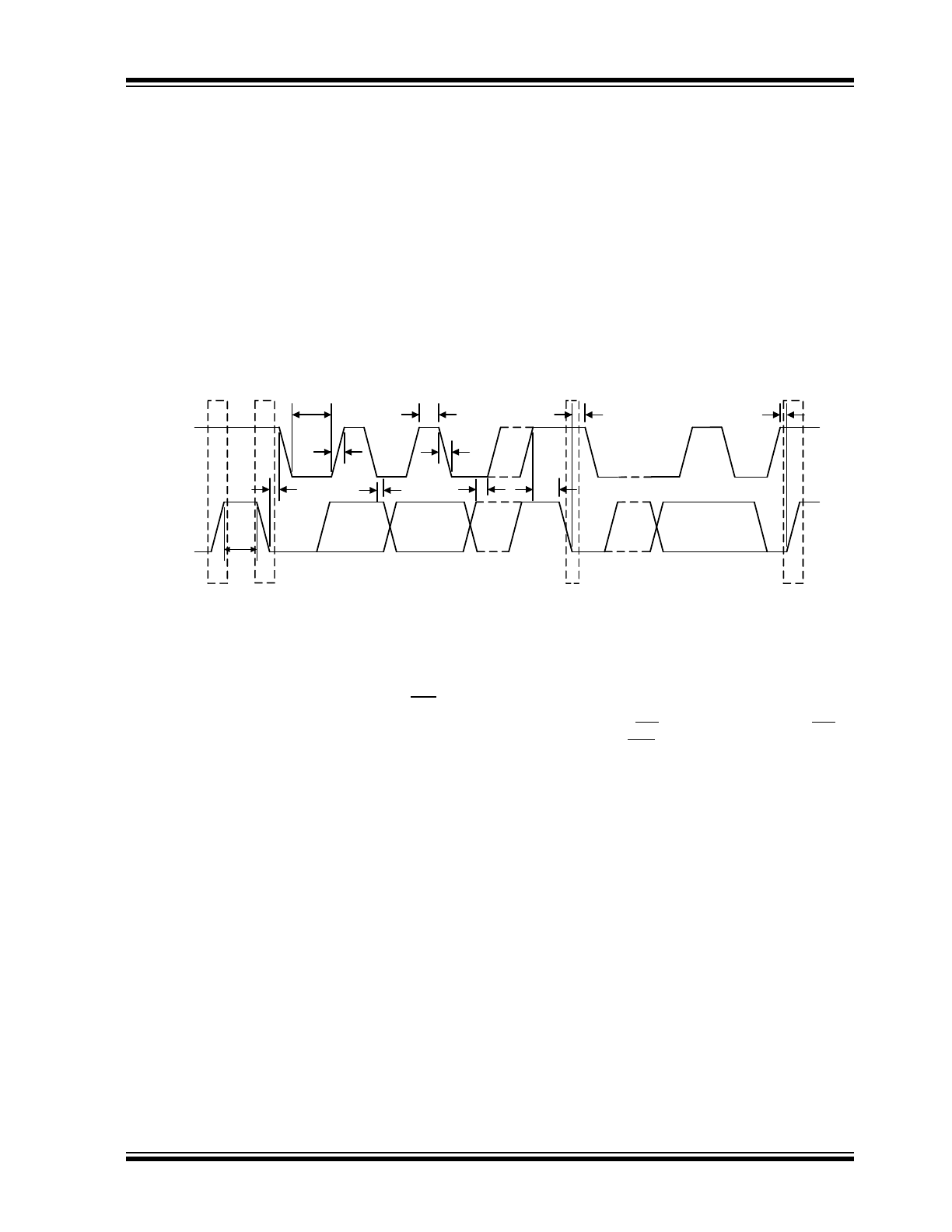
wire serial communication protocol between a computer host and its peripheral devices. A detailed timing diagram is
shown in
Figure 3-1
. Stretching of the SMCLK signal is supported; however, the CAP1203 will not stretch the clock sig-
nal.
3.2.1
SMBUS START BIT
The SMBus Start bit is defined as a transition of the SMBus Data line from a logic ‘1’ state to a logic ‘0’ state while the
SMBus Clock line is in a logic ‘1’ state.
3.2.2
SMBUS ADDRESS AND RD / WR BIT
The SMBus Address Byte consists of the 7-bit client address followed by the RD / WR indicator bit. If this RD / WR bit
is a logic ‘0’, then the SMBus Host is writing data to the client device. If this RD / WR bit is a logic ‘1’, then the SMBus
Host is reading data from the client device.
3.2.3
The CAP1203responds to SMBus address 0101_000(r/w).
SMBUS DATA BYTES
All SMBus Data bytes are sent most significant bit first and composed of 8-bits of information.
3.2.4
SMBUS ACK AND NACK BITS
The SMBus client will acknowledge all data bytes that it receives. This is done by the client device pulling the SMBus
Data line low after the 8th bit of each byte that is transmitted. This applies to both the Write Byte and Block Write proto-
cols.
The Host will NACK (not acknowledge) the last data byte to be received from the client by holding the SMBus data line
high after the 8th data bit has been sent. For the Block Read protocol, the Host will ACK each data byte that it receives
except the last data byte.
3.2.5
SMBUS STOP BIT
The SMBus Stop bit is defined as a transition of the SMBus Data line from a logic ‘0’ state to a logic ‘1’ state while the
SMBus clock line is in a logic ‘1’ state. When the CAP1203 detects an SMBus Stop bit and it has been communicating
with the SMBus protocol, it will reset its client interface and prepare to receive further communications.
FIGURE 3-1:
SMBUS TIMING DIAGRAM
SM D A TA
SM C LK
T
B U F
P
S
S - Start C o ndition
P - Stop C ondition
P
S
T
H IG H
T
LO W
T
H D :STA
T
SU :STO
T
H D :STA
T
H D :D AT
T
S U :D AT
T
SU :STA
T
FALL
T
R ISE

DS00001572B-page 10
2013-2015 Microchip Technology Inc.
3.2.6
SMBUS TIMEOUT
The CAP1203 includes an SMBus timeout feature. Following a 30ms period of inactivity on the SMBus where the
SMCLK pin is held low, the device will timeout and reset the SMBus interface.
The timeout function defaults to disabled. It can be enabled by setting the TIMEOUT bit in the Configuration register
(see
Section 5.6, "Configuration Registers"
).
3.2.7
SMBUS AND I
2
C COMPATIBILITY
The major differences between SMBus and I
2
C devices are highlighted here. For more information, refer to the SMBus
2.0 specification.
1.
CAP1203supports I
2
C fast mode at 400kHz. This covers the SMBus max time of 100kHz.
2.
Minimum frequency for SMBus communications is 10kHz.
3.
The SMBus client protocol will reset if the clock is held low longer than 30ms (timeout condition). This can be
enabled in the CAP1203 by setting the TIMEOUT bit in the Configuration register. I
2
C does not have a timeout.
4.
The SMBus client protocol will reset if both the clock and the data line are high for longer than 200us (idle con-
dition). This can be enabled in the CAP1203by setting the TIMEOUT bit in the Configuration register. I
2
C does
not have an idle condition.
5.
I
2
C devices do not support the Alert Response Address functionality (which is optional for SMBus).
6.
I
2
C devices support block read and write differently. I
2
C protocol allows for unlimited number of bytes to be sent
in either direction. The SMBus protocol requires that an additional data byte indicating number of bytes to read /
write is transmitted. The CAP1203 supports I
2
C formatting only.
3.3
SMBus Protocols
The CAP1203 is SMBus 2.0 compatible and supports Write Byte, Read Byte, Send Byte, and Receive Byte as valid
protocols as shown below.
All of the below protocols use the convention in
Table 3-1
.
3.3.1
SMBUS WRITE BYTE
The Write Byte is used to write one byte of data to a specific register as shown in
Table 3-2
.
3.3.2
SMBUS READ BYTE
The Read Byte protocol is used to read one byte of data from the registers as shown in
Table 3-3
.
TABLE 3-1:
PROTOCOL FORMAT
Data Sent to
Device
Data Sent to the
HOst
Data sent
Data sent
TABLE 3-2:
WRITE BYTE PROTOCOL
Start
Slave
Address
WR
ACK
Register
Address
ACK
Register
Data
ACK
Stop
1 ->0
0101_000
0
0
XXh
0
XXh
0
0 -> 1