

Features
•
High Performance, Low Power AVR
®
8-Bit Microcontroller
•
Advanced RISC Architecture
– 123 Powerful Instructions – Most Single Clock Cycle Execution
– 32 x 8 General Purpose Working Registers
– Fully Static Operation
•
High Endurance Non-volatile Memory Segments
– 4K/8K Bytes of In-System Self-Programmable Flash Program Memory
– 64/64 Bytes EEPROM
– 256/512 Bytes Internal SRAM
– Write/Erase Cycles: 10,000 Flash/100,000 EEPROM
– Data Retention: 20 years at 85
°C / 100 years at 25°C
– Programming Lock for Software Security
•
Peripheral Features
– One 8-bit Timer/Counter with Separate Prescaler and Compare Mode
– One 16-bit Timer/Counter with Prescaler, and Compare and Capture Modes
– 6- or 8-channel 10-bit ADC
– Master/Slave SPI Serial Interface
– Byte-oriented 2-wire Serial Interface (Philips I
2
C Compatible)
– Programmable Watchdog Timer with Separate On-Chip Oscillator
– On-Chip Analog Comparator
– Interrupt and Wake-up on Pin Change
•
Special Microcontroller Features
– debugWIRE On-Chip Debug System
– In-System Programmable via SPI Port
– Power-On Reset and Programmable Brown-Out Detection
– Internal Calibrated Oscillator
– External and Internal Interrupt Sources
– Three Sleep Modes: Idle, ADC Noise Reduction and Power-Down
– On-Chip Temperature Sensor
•
I/O and Packages
– 24 Programmable I/O Lines:
• 28-pin PDIP
• 28-pad QFN
– 28 Programmable I/O Lines:
• 32-lead TQFP
• 32-pad QFN
• 32-ball UFBGA
•
Operating Voltage:
– 1.8
–
5.5V
•
Temperature Range:
– -40
°
C to +85
°
C
•
Speed Grade:
– 0
–
4 MHz @ 1.8
–
5.5V
– 0
–
8 MHz @ 2.7
–
5.5V
– 0
–
12 MHz @ 4.5
–
5.5V
•
Low Power Consumption
– Active Mode: 1 MHz, 1.8V: 240 µA
– Power-Down Mode: 0.1 µA at 1.8V
8-bit
Microcontroller
with 4/8K Bytes
In-System
Programmable
Flash
ATtiny48/88
Summary
Rev. 8008HS–AVR–04/11
2
8008HS–AVR–04/11
ATtiny48/88
1.
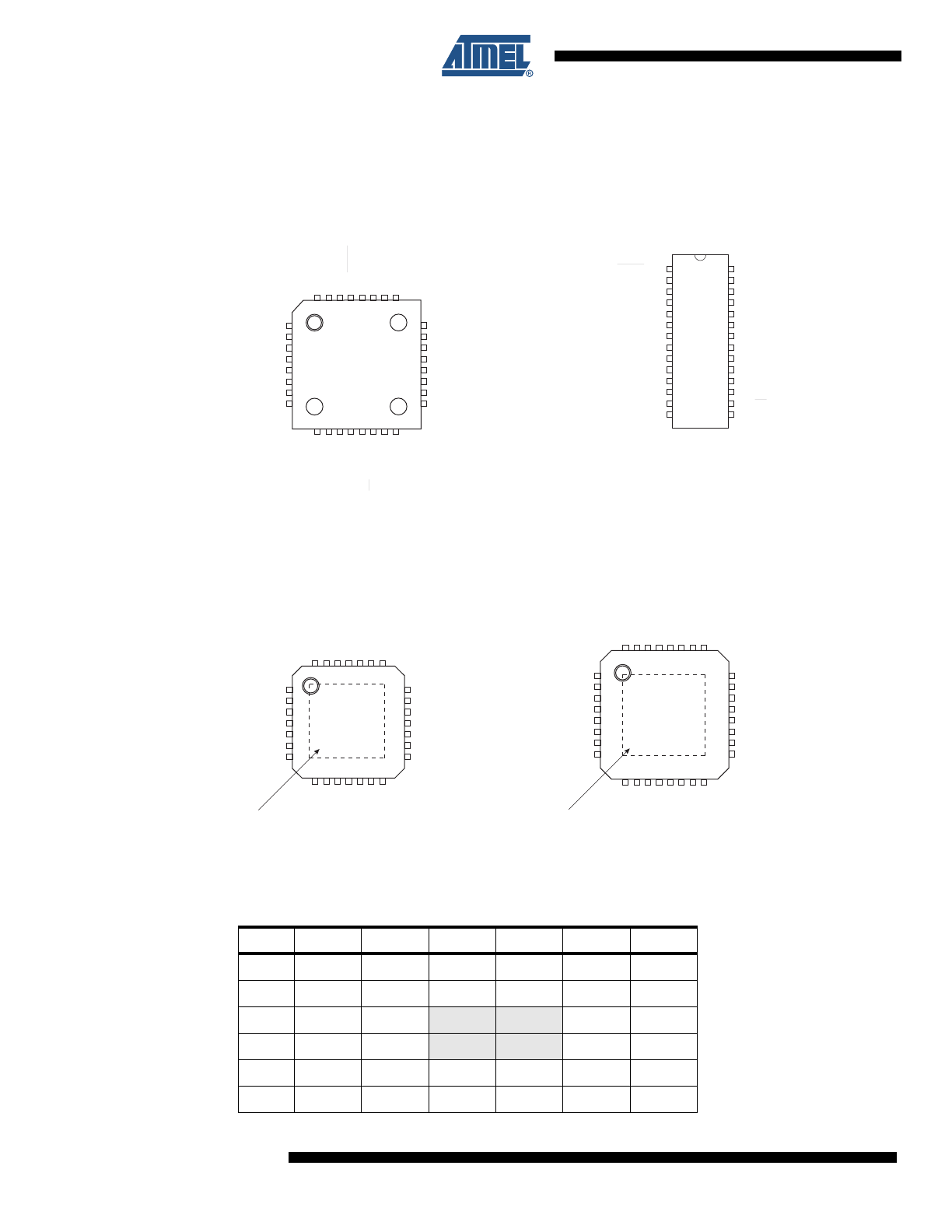
Pin Configurations
Figure 1-1.
Pinout of ATtiny48/88
1
2
3
4
5
6
7
8
24
23
22
21
20
19
18
17
(PCINT19/INT1) PD3
(PCINT20/T0) PD4
(PCINT26) PA2
VCC
GND
(PCINT27) PA3
(PCINT6/CLKI) PB6
(PCINT7) PB7
PC1 (ADC1/PCINT9)
PC0 (ADC0/PCINT8)
PA1 (ADC7/PCINT25)
GND
PC7 (PCINT15)
PA0 (ADC6/PCINT24)
AVCC
PB5 (SCK/PCINT5)
32
31
30
29
28
27
26
25
9
10
11
12
13
14
15
16
(PCINT21/T1) PD5
(PCINT22/AIN0) PD6
(PCINT23/AIN1) PD7
(PCINT0/CLK
O/ICP1) PB0
(PCINT1/OC1A) PB1
(PCINT2/SS/OC1B) PB2
(PCINT3/MOSI) PB3
(PCINT4/MISO) PB4
PD2 (INT0/PCINT18)
PD1 (PCINT17)
PD0 (PCINT16)
PC6 (RESET/PCINT14)
PC5 (ADC5/SCL/PCINT13)
PC4 (ADC4/SD
A/PCINT12)
PC3 (ADC3/PCINT11)
PC2 (ADC2/PCINT10)
TQFP Top View
1
2
3
4
5
6
7
8
9
10
11
12
13
14
28
27
26
25
24
23
22
21
20
19
18
17
16
15
(PCINT14/RESET) PC6
(PCINT16) PD0
(PCINT17) PD1
(PCINT18/INT0) PD2
(PCINT19/INT1) PD3
(PCINT20/T0) PD4
VCC
GND
(PCINT6/CLKI) PB6
(PCINT7) PB7
(PCINT21/T1) PD5
(PCINT22/AIN0) PD6
(PCINT23/AIN1) PD7
(PCINT0/CLKO/ICP1) PB0
PC5 (ADC5/SCL/PCINT13)
PC4 (ADC4/SDA/PCINT12)
PC3 (ADC3/PCINT11)
PC2 (ADC2/PCINT10)
PC1 (ADC1/PCINT9)
PC0 (ADC0/PCINT8)
GND
PC7 (PCINT15)
AVCC
PB5 (SCK/PCINT5)
PB4 (MISO/PCINT4)
PB3 (MOSI/PCINT3)
PB2 (SS/OC1B/PCINT2)
PB1 (OC1A/PCINT1)
PDIP
1
2
3
4
5
6
7
8
24
23
22
21
20
19
18
17
32
31
30
29
28
27
26
25
9
10
11
12
13
14
15
16
32 QFN Top View
(PCINT19/INT1) PD3
(PCINT20/T0) PD4
(PCINT26) PA2
VCC
GND
(PCINT27) PA3
(PCINT6/CLKI) PB6
(PCINT7) PB7
PC1 (ADC1/PCINT9)
PC0 (ADC0/PCINT8)
PA1 (ADC7/PCINT25)
GND
PC7 (PCINT15)
PA0 (ADC6/PCINT24)
AVCC
PB5 (SCK/PCINT5)
(PCINT21/T1) PD5
(PCINT22/AIN0) PD6
(PCINT23/AIN1) PD7
(PCINT0/CLK
O/ICP1) PB0
(PCINT1/OC1A) PB1
(PCINT2/SS/OC1B) PB2
(PCINT3/MOSI) PB3
(PCINT4/MISO) PB4
PD2 (INT0/PCINT18)
PD1 (PCINT17)
PD0 (PCINT16)
PC6 (RESET/PCINT14)
PC5 (ADC5/SCL/PCINT13)
PC4 (ADC4/SD
A/PCINT12)
PC3 (ADC3/PCINT11)
PC2 (ADC2/PCINT10)
NOTE: Bottom pad should be soldered to ground.
1
2
3
4
5
6
7
21
20
19
18
17
16
15
28
27
26
25
24
23
22
8
9
10
11
12
13
14
28 QFN Top View
(PCINT19/INT1) PD3
(PCINT20/T0) PD4
VCC
GND
(PCINT6/CLKI) PB6
(PCINT7) PB7
(PCINT21/T1) PD5
(PCINT22/AIN0) PD6
(PCINT23/AIN1) PD7
(PCINT0/CLK
O/ICP1) PB0
(PCINT1/OC1A) PB1
(PCINT2/SS/OC1B) PB2
(PCINT3//MOSI) PB3
(PCINT4/MISO) PB4
PD2 (INT0/PCINT18)
PD1 (PCINT17)
PD0 (PCINT16)
PC6 (RESET/PCINT14)
PC5 (ADC5/SCL/PCINT13)
PC4 (ADC4/SD
A/PCINT12)
PC3 (ADC3/PCINT11)
PC2 (ADC2/PCINT10)
PC1 (ADC1/PCINT9)
PC0 (ADC0/PCINT8)
GND
PC7 (PCI NT15)
AVCC
PB5 (SCK/PCINT5)
NOTE: Bottom pad should be soldered to ground.
Table 1-1.
32 UFBGA Top View. See
page 288
.
1
2
3
4
5
6
A
PD2
PD1
PC6
PC4
PC2
PC1
B
PD3
PD4
PD0
PC5
PC3
PC0
C
GND
PA2
PA1
GND
D
VCC
PA3
PC7
PA0
E
PB6
PD6
PB0
PB2
AVCC
PB5
F
PB7
PD5
PD7
PB1
PB3
PB4

3
8008HS–AVR–04/11
ATtiny48/88
1.1
Pin Descriptions
1.1.1
VCC
Digital supply voltage.
1.1.2
AVCC
AV
CC
is the supply voltage pin for the A/D converter and a selection of I/O pins. This pin should
be externally connected to V
CC
even if the ADC is not used. If the ADC is used, it is recom-
mended this pin is connected to V
CC
through a low-pass filter, as described in
“Analog Noise
Canceling Techniques” on page 172
.
The following pins receive their supply voltage from AV
CC
: PC7, PC[5:0] and (in 32-lead pack-
ages) PA[1:0]. All other I/O pins take their supply voltage from V
CC
.
1.1.3
GND
Ground.
1.1.4
Port A (PA3:0)
Port A is a 4-bit bi-directional I/O port with internal pull-up resistors (selected for each bit). The
PA[3:0] output buffers have symmetrical drive characteristics with both sink and source capabil-
ity. As inputs, Port A pins that are externally pulled low will source current if the pull-up resistors
are activated. The Port A pins are tri-stated when a reset condition becomes active, even if the
clock is not running.
This port is available in 32-lead TQFP, 32-pad QFN and 32-ball UFBGA packages, only.
1.1.5
Port B (PB7:0)
Port B is an 8-bit bi-directional I/O port with internal pull-up resistors (selected for each bit). The
Port B output buffers have symmetrical drive characteristics with both sink and source capability.
As inputs, Port B pins that are externally pulled low will source current if the pull-up resistors are
activated. The Port B pins are tri-stated when a reset condition becomes active, even if the clock
is not running.
Depending on the clock selection fuse settings, PB6 can be used as input to the internal clock
operating circuit.
The various special features of Port B are elaborated in
“Alternate Functions of Port B” on page
69
.
1.1.6
Port C (PC7, PC5:0)
Port C is a 8-bit bi-directional I/O port with internal pull-up resistors (selected for each bit). The
PC7 and PC[5:0] output buffers have symmetrical drive characteristics with both sink and source
capability. As inputs, Port C pins that are externally pulled low will source current if the pull-up
resistors are activated. The Port C pins are tri-stated when a reset condition becomes active,
even if the clock is not running.
1.1.7
PC6/RESET
If the RSTDISBL Fuse is programmed, PC6 is used as an I/O pin. Note that the electrical char-
acteristics of PC6 differ from those of the other pins of Port C.
If the RSTDISBL Fuse is unprogrammed, PC6 is used as a reset input. A low level on this pin for
longer than the minimum pulse width will generate a reset, even if the clock is not running. The

4
8008HS–AVR–04/11
ATtiny48/88
minimum pulse length is given in
Table 22-3 on page 209
. Shorter pulses are not guaranteed to
generate a reset.
The various special features of Port C are elaborated in
“Alternate Functions of Port C” on page
72
.
1.1.8
Port D (PD7:0)
Port D is an 8-bit bi-directional I/O port with internal pull-up resistors (selected for each bit). The
PD[7:4] output buffers have symmetrical drive characteristics with both sink and source capabil-
ities, while the PD[3:0] output buffers have high sink capabilities. As inputs, Port D pins that are
externally pulled low will source current if the pull-up resistors are activated. The Port D pins are
tri-stated when a reset condition becomes active, even if the clock is not running.
The various special features of Port D are elaborated in
“Alternate Functions of Port D” on page
75
.
5
8008HS–AVR–04/11
ATtiny48/88
2.
Overview
The ATtiny48/88 is a low-power CMOS 8-bit microcontroller based on the AVR enhanced RISC
architecture. By executing powerful instructions in a single clock cycle, the ATtiny48/88 achieves
throughputs approaching 1 MIPS per MHz allowing the system designer to optimize power con-
sumption versus processing speed.
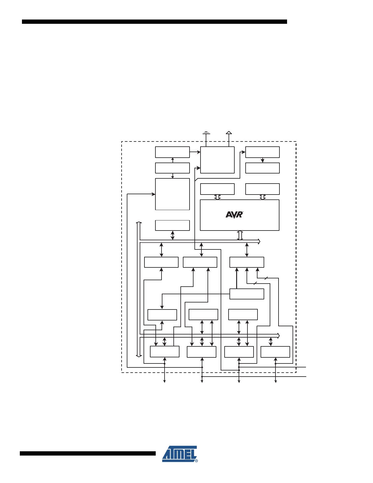
2.1
Block Diagram
Figure 2-1.
Block Diagram
The AVR core combines a rich instruction set with 32 general purpose working registers. All the
32 registers are directly connected to the Arithmetic Logic Unit (ALU), allowing two independent
registers to be accessed in one single instruction executed in one clock cycle. The resulting
architecture is more code efficient while achieving throughputs up to ten times faster than con-
ventional CISC microcontrollers.
PORT C (8)
PORT B (8)
PORT D (8)
16bit T/C 1
8bit T/C 0
A/D Conv.
Internal
Bandgap
Analog
Comp.
SPI
TWI
SRAM
Flash
EEPROM
Watchdog
Oscillator
Watchdog
Timer
Oscillator
Circuits /
Clock
Generation
Power
Supervision
POR / BOD &
RESET
VC
C
GND
Program
Logic
debugWIRE
2
D
A
TABUS
PA[0:3] (in TQFP and MLF)
PC[0:7]
PB[0:7]
PD[0:7]
6
RESET
CLKI
CPU
PORT A (4)

6
8008HS–AVR–04/11
ATtiny48/88
The ATtiny48/88 provides the following features:
• 4/8K bytes of In-System Programmable Flash
• 64/64 bytes EEPROM
• 256/512 bytes SRAM
• 24 general purpose I/O lines
– 28 in 32-lead TQFP, 32-pad QFN, and 32-ball UFBGA packages
• 32 general purpose working registers
• Two flexible Timer/Counters with compare modes
• Internal and external interrupts
• A byte-oriented, 2-wire serial interface
• An SPI serial port
• A 6-channel, 10-bit ADC
– 8 in 32-lead TQFP, 32-pad QFN, and 32-ball UFBGA packages
• A programmable Watchdog Timer with internal oscillator
• Three software selectable power saving modes.
The device includes the following modes for saving power:
• Idle mode: stops the CPU while allowing the timer/counter, ADC, analog comparator, SPI,
TWI, and interrupt system to continue functioning
• ADC Noise Reduction mode: minimizes switching noise during ADC conversions by stopping
the CPU and all I/O modules except the ADC
• Power-down mode: registers keep their contents and all chip functions are disabled until the
next interrupt or hardware reset
The device is manufactured using Atmel’s high density non-volatile memory technology. The
On-chip ISP Flash allows the program memory to be reprogrammed In-System through an SPI
serial interface, by a conventional non-volatile memory programmer, or by an on-chip boot pro-
gram running on the AVR core. The boot program can use any interface to download the
application program in the Flash memory. By combining an 8-bit RISC CPU with In-System Self-
Programmable Flash on a monolithic chip, the Atmel ATtiny48/88 is a powerful microcontroller
that provides a highly flexible and cost effective solution to many embedded control applications.
The ATtiny48/88 AVR is supported by a full suite of program and system development tools
including: C compilers, macro assemblers, program debugger/simulators and evaluation kits.
2.2
Comparison Between ATtiny48 and ATtiny88
The ATtiny48 and ATtiny88 differ only in memory sizes, as summarised in
Table 2-1
, below.
Table 2-1.
Memory Size Summary
Device
Flash
EEPROM
RAM
ATtiny48
4K Bytes
64 Bytes
256 Bytes
ATtiny88
8K Bytes
64 Bytes
512 Bytes

7
8008HS–AVR–04/11
ATtiny48/88
3.
General Information
3.1
Resources
A comprehensive set of development tools, application notes and datasheets are available for
download at http://www.atmel.com/avr.
3.2
About Code Examples
This documentation contains simple code examples that briefly show how to use various parts of
the device. These code examples assume that the part specific header file is included before
compilation. Be aware that not all C compiler vendors include bit definitions in the header files
and interrupt handling in C is compiler dependent. Please confirm with the C compiler documen-
tation for more details.
For I/O Registers located in extended I/O map, “IN”, “OUT”, “SBIS”, “SBIC”, “CBI”, and “SBI”
instructions must be replaced with instructions that allow access to extended I/O. Typically
“LDS” and “STS” combined with “SBRS”, “SBRC”, “SBR”, and “CBR”.
3.3
Capacitive Touch Sensing
Atmel QTouch Library provides a simple to use solution for touch sensitive interfaces on Atmel
AVR microcontrollers. The QTouch Library includes support for QTouch
®
and QMatrix
®
acquisi-
tion methods.
Touch sensing is easily added to any application by linking the QTouch Library and using the
Application Programming Interface (API) of the library to define the touch channels and sensors.
The application then calls the API to retrieve channel information and determine the state of the
touch sensor.
The QTouch Library is free and can be downloaded from the Atmel website. For more informa-
tion and details of implementation, refer to the QTouch Library User Guide – also available from
the Atmel website.
3.4
Data Retention
Reliability Qualification results show that the projected data retention failure rate is much less
than 1 PPM over 20 years at 85°C or 100 years at 25°C.
3.5
Disclaimer
Typical values contained in this datasheet are based on simulations and characterization of
other AVR microcontrollers manufactured on the same process technology.
8
8008HS–AVR–04/11
ATtiny48/88
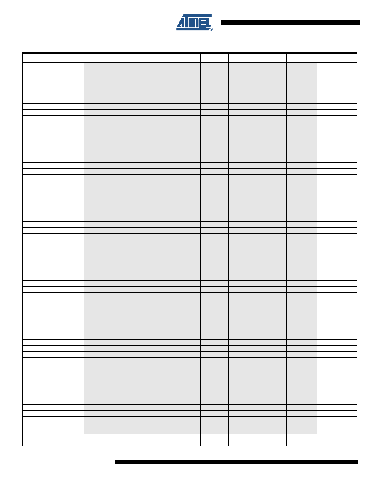
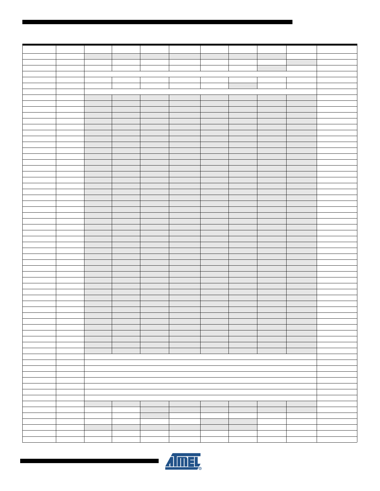
4.
Register Summary
Address
Name
Bit 7
Bit 6
Bit 5
Bit 4
Bit 3
Bit 2
Bit 1
Bit 0
Page
(0xFF)
Reserved
–
–
–
–
–
–
–
–
(0xFE)
Reserved
–
–
–
–
–
–
–
–
(0xFD)
Reserved
–
–
–
–
–
–
–
–
(0xFC)
Reserved
–
–
–
–
–
–
–
–
(0xFB)
Reserved
–
–
–
–
–
–
–
–
(0xFA)
Reserved
–
–
–
–
–
–
–
–
(0xF9)
Reserved
–
–
–
–
–
–
–
–
(0xF8)
Reserved
–
–
–
–
–
–
–
–
(0xF7)
Reserved
–
–
–
–
–
–
–
–
(0xF6)
Reserved
–
–
–
–
–
–
–
–
(0xF5)
Reserved
–
–
–
–
–
–
–
–
(0xF4)
Reserved
–
–
–
–
–
–
–
–
(0xF3)
Reserved
–
–
–
–
–
–
–
–
(0xF2)
Reserved
–
–
–
–
–
–
–
–
(0xF1)
Reserved
–
–
–
–
–
–
–
–
(0xF0)
Reserved
–
–
–
–
–
–
–
–
(0xEF)
Reserved
–
–
–
–
–
–
–
–
(0xEE)
Reserved
–
–
–
–
–
–
–
–
(0xED)
Reserved
–
–
–
–
–
–
–
–
(0xEC)
Reserved
–
–
–
–
–
–
–
–
(0xEB)
Reserved
–
–
–
–
–
–
–
–
(0xEA)
Reserved
–
–
–
–
–
–
–
–
(0xE9)
Reserved
–
–
–
–
–
–
–
–
(0xE8)
Reserved
–
–
–
–
–
–
–
–
(0xE7)
Reserved
–
–
–
–
–
–
–
–
(0xE6)
Reserved
–
–
–
–
–
–
–
–
(0xE5)
Reserved
–
–
–
–
–
–
–
–
(0xE4)
Reserved
–
–
–
–
–
–
–
–
(0xE3)
Reserved
–
–
–
–
–
–
–
–
(0xE2)
Reserved
–
–
–
–
–
–
–
–
(0xE1)
Reserved
–
–
–
–
–
–
–
–
(0xE0)
Reserved
–
–
–
–
–
–
–
–
(0xDF)
Reserved
–
–
–
–
–
–
–
–
(0xDE)
Reserved
–
–
–
–
–
–
–
–
(0xDD)
Reserved
–
–
–
–
–
–
–
–
(0xDC)
Reserved
–
–
–
–
–
–
–
–
(0xDB)
Reserved
–
–
–
–
–
–
–
–
(0xDA)
Reserved
–
–
–
–
–
–
–
–
(0xD9)
Reserved
–
–
–
–
–
–
–
–
(0xD8)
Reserved
–
–
–
–
–
–
–
–
(0xD7)
Reserved
–
–
–
–
–
–
–
–
(0xD6)
Reserved
–
–
–
–
–
–
–
–
(0xD5)
Reserved
–
–
–
–
–
–
–
–
(0xD4)
Reserved
–
–
–
–
–
–
–
–
(0xD3)
Reserved
–
–
–
–
–
–
–
–
(0xD2)
Reserved
–
–
–
–
–
–
–
–
(0xD1)
Reserved
–
–
–
–
–
–
–
–
(0xD0)
Reserved
–
–
–
–
–
–
–
–
(0xCF)
Reserved
–
–
–
–
–
–
–
–
(0xCE)
Reserved
–
–
–
–
–
–
–
–
(0xCD)
Reserved
–
–
–
–
–
–
–
–
(0xCC)
Reserved
–
–
–
–
–
–
–
–
(0xCB)
Reserved
–
–
–
–
–
–
–
–
(0xCA)
Reserved
–
–
–
–
–
–
–
–
(0xC9)
Reserved
–
–
–
–
–
–
–
–
(0xC8)
Reserved
–
–
–
–
–
–
–
–
(0xC7)
Reserved
–
–
–
–
–
–
–
–
(0xC6)
Reserved
–
–
–
–
–
–
–
–
(0xC5)
Reserved
–
–
–
–
–
–
–
–
(0xC4)
Reserved
–
–
–
–
–
–
–
–
(0xC3)
Reserved
–
–
–
–
–
–
–
–
(0xC2)
Reserved
–
–
–
–
–
–
–
–
(0xC1)
Reserved
–
–
–
–
–
–
–
–
(0xC0)
Reserved
–
–
–
–
–
–
–
–
(0xBF)
Reserved
–
–
–
–
–
–
–
–
9
8008HS–AVR–04/11
ATtiny48/88
(0xBE)
TWHSR
–
–
–
–
–
–
–
TWHS
160
(0xBD)
TWAMR
TWAM6
TWAM5
TWAM4
TWAM3
TWAM2
TWAM1
TWAM0
–
160
(0xBC)
TWCR
TWINT
TWEA
TWSTA
TWSTO
TWWC
TWEN
–
TWIE
156
(0xBB)
TWDR
2-wire Serial Interface Data Register
159
(0xBA)
TWAR
TWA6
TWA5
TWA4
TWA3
TWA2
TWA1
TWA0
TWGCE
159
(0xB9)
TWSR
TWS7
TWS6
TWS5
TWS4
TWS3
–
TWPS1
TWPS0
158
(0xB8)
TWBR
2-wire Serial Interface Bit Rate Register
156
(0xB7)
Reserved
–
–
–
–
–
–
–
–
(0xB6)
Reserved
–
–
–
–
–
–
–
–
(0xB5)
Reserved
–
–
–
–
–
–
–
–
(0xB4)
Reserved
–
–
–
–
–
–
–
–
(0xB3)
Reserved
–
–
–
–
–
–
–
–
(0xB2)
Reserved
–
–
–
–
–
–
–
–
(0xB1)
Reserved
–
–
–
–
–
–
–
–
(0xB0)
Reserved
–
–
–
–
–
–
–
–
(0xAF)
Reserved
–
–
–
–
–
–
–
–
(0xAE)
Reserved
–
–
–
–
–
–
–
–
(0xAD)
Reserved
–
–
–
–
–
–
–
–
(0xAC)
Reserved
–
–
–
–
–
–
–
–
(0xAB)
Reserved
–
–
–
–
–
–
–
–
(0xAA)
Reserved
–
–
–
–
–
–
–
–
(0xA9)
Reserved
–
–
–
–
–
–
–
–
(0xA8)
Reserved
–
–
–
–
–
–
–
–
(0xA7)
Reserved
–
–
–
–
–
–
–
–
(0xA6)
Reserved
–
–
–
–
–
–
–
–
(0xA5)
Reserved
–
–
–
–
–
–
–
–
(0xA4)
Reserved
–
–
–
–
–
–
–
–
(0xA3)
Reserved
–
–
–
–
–
–
–
–
(0xA2)
Reserved
–
–
–
–
–
–
–
–
(0xA1)
Reserved
–
–
–
–
–
–
–
–
(0xA0)
Reserved
–
–
–
–
–
–
–
–
(0x9F)
Reserved
–
–
–
–
–
–
–
–
(0x9E)
Reserved
–
–
–
–
–
–
–
–
(0x9D)
Reserved
–
–
–
–
–
–
–
–
(0x9C)
Reserved
–
–
–
–
–
–
–
–
(0x9B)
Reserved
–
–
–
–
–
–
–
–
(0x9A)
Reserved
–
–
–
–
–
–
–
–
(0x99)
Reserved
–
–
–
–
–
–
–
–
(0x98)
Reserved
–
–
–
–
–
–
–
–
(0x97)
Reserved
–
–
–
–
–
–
–
–
(0x96)
Reserved
–
–
–
–
–
–
–
–
(0x95)
Reserved
–
–
–
–
–
–
–
–
(0x94)
Reserved
–
–
–
–
–
–
–
–
(0x93)
Reserved
–
–
–
–
–
–
–
–
(0x92)
Reserved
–
–
–
–
–
–
–
–
(0x91)
Reserved
–
–
–
–
–
–
–
–
(0x90)
Reserved
–
–
–
–
–
–
–
–
(0x8F)
Reserved
–
–
–
–
–
–
–
–
(0x8E)
Reserved
–
–
–
–
–
–
–
–
(0x8D)
Reserved
–
–
–
–
–
–
–
–
(0x8C)
Reserved
–
–
–
–
–
–
–
–
(0x8B)
OCR1BH
Timer/Counter1
–
Output Compare Register B High Byte
114
(0x8A)
OCR1BL
Timer/Counter1
–
Output Compare Register B Low Byte
114
(0x89)
OCR1AH
Timer/Counter1
–
Output Compare Register A High Byte
114
(0x88)
OCR1AL
Timer/Counter1
–
Output Compare Register A Low Byte
114
(0x87)
ICR1H
Timer/Counter1
–
Input Capture Register High Byte
114
(0x86)
ICR1L
Timer/Counter1
–
Input Capture Register Low Byte
114
(0x85)
TCNT1H
Timer/Counter1
–
Counter Register High Byte
113
(0x84)
TCNT1L
Timer/Counter1
–
Counter Register Low Byte
113
(0x83)
Reserved
–
–
–
–
–
–
–
–
(0x82)
TCCR1C
FOC1A
FOC1B
–
–
–
–
–
–
113
(0x81)
TCCR1B
ICNC1
ICES1
–
WGM13
WGM12
CS12
CS11
CS10
112
(0x80)
TCCR1A
COM1A1
COM1A0
COM1B1
COM1B0
–
–
WGM11
WGM10
110
(0x7F)
DIDR1
–
–
–
–
–
–
AIN1D
AIN0D
163
(0x7E)
DIDR0
ADC7D
ADC6D
ADC5D
ADC4D
ADC3D
ADC2D
ADC1D
ADC0D
180
(0x7D)
Reserved
–
–
–
–
–
–
–
–
Address
Name
Bit 7
Bit 6
Bit 5
Bit 4
Bit 3
Bit 2
Bit 1
Bit 0
Page
10
8008HS–AVR–04/11
ATtiny48/88
(0x7C)
ADMUX
–
REFS0
ADLAR
–
MUX3
MUX2
MUX1
MUX0
176
(0x7B)
ADCSRB
–
ACME
–
–
–
ADTS2
ADTS1
ADTS0
162, 179
(0x7A)
ADCSRA
ADEN
ADSC
ADATE
ADIF
ADIE
ADPS2
ADPS1
ADPS0
178
(0x79)
ADCH
ADC Data Register High byte
179
(0x78)
ADCL
ADC Data Register Low byte
179
(0x77)
Reserved
–
–
–
–
–
–
–
–
(0x76)
Reserved
–
–
–
–
–
–
–
–
(0x75)
Reserved
–
–
–
–
–
–
–
–
(0x74)
Reserved
–
–
–
–
–
–
–
–
(0x73)
Reserved
–
–
–
–
–
–
–
–
(0x72)
Reserved
–
–
–
–
–
–
–
–
(0x71)
Reserved
–
–
–
–
–
–
–
–
(0x70)
Reserved
–
–
–
–
–
–
–
–
(0x6F)
TIMSK1
–
–
ICIE1
–
–
OCIE1B
OCIE1A
TOIE1
114
(0x6E)
TIMSK0
–
–
–
–
–
OCIE0B
OCIE0A
TOIE0
87
(0x6D)
PCMSK2
PCINT23
PCINT22
PCINT21
PCINT20
PCINT19
PCINT18
PCINT17
PCINT16
59
(0x6C)
PCMSK1
PCINT15
PCINT14
PCINT13
PCINT12
PCINT11
PCINT10
PCINT9
PCINT8
59
(0x6B)
PCMSK0
PCINT7
PCINT6
PCINT5
PCINT4
PCINT3
PCINT2
PCINT1
PCINT0
59
(0x6A)
PCMSK3
–
–
-
-
PCINT27
PCINT26
PCINT25
PCINT24
59
(0x69)
EICRA
–
–
–
–
ISC11
ISC10
ISC01
ISC00
55
(0x68)
PCICR
–
–
–
–
PCIE3
PCIE2
PCIE1
PCIE0
57
(0x67)
Reserved
–
–
–
–
–
–
–
–
(0x66)
OSCCAL
Oscillator Calibration Register
34
(0x65)
Reserved
–
–
–
–
–
–
–
–
(0x64)
PRR
PRTWI
–
PRTIM0
–
PRTIM1
PRSPI
–
PRADC
40
(0x63)
Reserved
–
–
–
–
–
–
–
–
(0x62)
Reserved
–
–
–
–
–
–
–
–
(0x61)
CLKPR
CLKPCE
–
–
–
CLKPS3
CLKPS2
CLKPS1
CLKPS0
34
(0x60)
WDTCSR
WDIF
WDIE
WDP3
WDCE
WDE
WDP2
WDP1
WDP0
49
0x3F (0x5F)
SREG
I
T
H
S
V
N
Z
C
9
0x3E (0x5E)
SPH
–
–
–
–
–
–
SP9
SP8
11
0x3D (0x5D)
SPL
SP7
SP6
SP5
SP4
SP3
SP2
SP1
SP0
11
0x3C (0x5C)
Reserved
–
–
–
–
–
–
–
–
0x3B (0x5B)
Reserved
–
–
–
–
–
–
–
–
0x3A (0x5A)
Reserved
–
–
–
–
–
–
–
–
0x39 (0x59)
Reserved
–
–
–
–
–
–
–
–
0x38 (0x58)
Reserved
–
–
–
–
–
–
–
–
0x37 (0x57)
SPMCSR
–
RWWSB
–
CTPB
RFLB
PGWRT
PGERS
SELFPRGEN
186
0x36 (0x56)
Reserved
–
–
–
–
–
0x35 (0x55)
MCUCR
–
BODS
BODSE
PUD
–
–
–
–
40, 77
0x34 (0x54)
MCUSR
–
–
–
–
WDRF
BORF
EXTRF
PORF
49
0x33 (0x53)
SMCR
–
–
–
–
–
SM1
SM0
SE
39
0x32 (0x52)
Reserved
–
–
–
–
–
–
–
–
0x31 (0x51)
DWDR
debugWire Data Register
182
0x30 (0x50)
ACSR
ACD
ACBG
ACO
ACI
ACIE
ACIC
ACIS1
ACIS0
162
0x2F (0x4F)
Reserved
–
–
–
–
–
–
–
–
0x2E (0x4E)
SPDR
SPI Data Register
128
0x2D (0x4D)
SPSR
SPIF
WCOL
–
–
–
–
–
SPI2X
127
0x2C (0x4C)
SPCR
SPIE
SPE
DORD
MSTR
CPOL
CPHA
SPR1
SPR0
126
0x2B (0x4B)
GPIOR2
General Purpose I/O Register 2
27
0x2A (0x4A)
GPIOR1
General Purpose I/O Register 1
27
0x29 (0x49)
Reserved
–
–
–
–
–
–
–
–
0x28 (0x48)
OCR0B
Timer/Counter0 Output Compare Register B
87
0x27 (0x47)
OCR0A
Timer/Counter0 Output Compare Register A
86
0x26 (0x46)
TCNT0
Timer/Counter0 (8-bit)
86
0x25 (0x45)
TCCR0A
–
–
–
–
CTC0
CS02
CS01
CS00
85
0x24 (0x44)
Reserved
–
–
–
–
–
–
–
–
0x23 (0x43)
GTCCR
TSM
–
–
–
–
–
–
PSRSYNC
118
0x22 (0x42)
Reserved
–
–
–
–
–
–
–
–
0x21 (0x41)
EEARL
EEPROM Address Register Low Byte
25
0x20 (0x40)
EEDR
EEPROM Data Register
25
0x1F (0x3F)
EECR
–
–
EEPM1
EEPM0
EERIE
EEMPE
EEPE
EERE
25
0x1E (0x3E)
GPIOR0
General Purpose I/O Register 0
27
0x1D (0x3D)
EIMSK
–
–
–
–
–
–
INT1
INT0
56
0x1C (0x3C)
EIFR
–
–
–
–
–
–
INTF1
INTF0
56
0x1B (0x3B)
PCIFR
–
–
–
–
PCIF3
PCIF2
PCIF1
PCIF0
58
Address
Name
Bit 7
Bit 6
Bit 5
Bit 4
Bit 3
Bit 2
Bit 1
Bit 0
Page