
2010 Microchip Technology Inc.
DS21375D-page 1
TC1264
Features:
• Very Low Dropout Voltage
• 800 mA Output Current
• High Output Voltage Accuracy
• Standard or Custom Output Voltages
• Overcurrent and Overtemperature Protection
Applications:
• Battery Operated Systems
• Portable Computers
• Medical Instruments
• Instrumentation
• Cellular/GSM/PHS Phones
• Linear Post-Regulators for SMPS
• Pagers
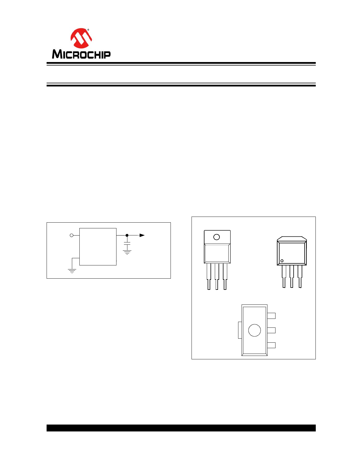
Typical Application
Description:
The TC1264 is a fixed-output, high-accuracy (typically
±0.5%) CMOS low dropout regulator. Designed
specifically for battery-operated systems, the TC1264’s
CMOS construction eliminates wasted ground current,
significantly extending battery life. Total supply current
is typically 80 µA at full load (20 to 60 times lower than
in bipolar regulators).
TC1264 key features include ultra low noise operation,
very low dropout voltage (typically 450 mV at full load),
and fast response to step changes in load.
The TC1264 incorporates both over temperature and
over current protection. The TC1264 is stable with an
output capacitor of only 1 µF and has a maximum
output current of 800 mA. It is available in 3-pin
SOT-223, 3-pin TO-220 and 3-pin DDPAK packages.
Package Type
TC1264
V
IN
V
OUT
C
1
1 µF
GND
V
OUT
V
IN
+
V
IN
V
IN
V
OUT
GND
GND
V
OU
T
T
AB IS
GND
FRONT VIEW
FRONT VIEW
1
1
2
3
3
2
3-Pin TO-220
TAB IS GND
3-Pin SOT-223
3-Pin DDPAK
1
2
3
TC1264
TC1264
TC1264
V
IN
GND
V
OU
T
800 mA Fixed-Output CMOS LDO with Shutdown
TC1264
DS21375D-page 2
2010 Microchip Technology Inc.
1.0
ELECTRICAL
CHARACTERISTICS
Absolute Maximum Ratings †
Input Voltage .........................................................6.5V
Output Voltage.................. (V
SS
– 0.3V) to (V
IN
+ 0.3V)
Power Dissipation................Internally Limited (
Note 8
)
Maximum Voltage on Any Pin ........V
IN
+0.3V to -0.3V
Operating Temperature Range...... -40°C < T
J
< 125°C
Storage Temperature..........................-65°C to +150°C
† Notice: Stresses above those listed under "Maximum
Ratings" may cause permanent damage to the device. This is
a stress rating only and functional operation of the device at
those or any other conditions above those indicated in the
operation listings of this specification is not implied. Exposure
to maximum rating conditions for extended periods may affect
device reliability.
DC CHARACTERISTICS
Electrical Specifications: Unless otherwise indicated, V
IN
= V
R
+ 1.5V, (
Note 1
), I
L
= 100 µA, C
L
= 3.3 µF, SHDN > V
IH
,
T
A
= +25°C. Boldface type specifications apply for junction temperatures of -40°C to +125°C.
Parameters
Sym
Min
Typ
Max
Units
Conditions
Input Operating Voltage
V
IN
2.7
—
6.0
V
Note 2
Maximum Output Current
I
OUTMAX
800
—
—
mA
Output Voltage
V
OUT
V
R
– 2.5%
V
R
± 0.5% V
R
+ 2.5%
V
V
R
2.5V
V
R
– 2%
V
R
± 0.5%
V
R
+ 3%
V
R
= 1.8V
V
R
– 7%
—
V
R
+ 3%
I
L
= 0.1 mA to 800 mA
(
Note 3
)
V
OUT
Temperature Coefficient
V
OUT
/
T
—
40
—
ppm/°C
Note 4
Line Regulation
V
OUT
/
V
IN
—
0.007
0.35
%
(V
R
+ 1V)
V
IN
6V
Load Regulation (
Note 5
)
V
OUT
/V
OUT
-0.01
0.002
0
%/mA
I
L
= 0.1 mA to I
OUTMAX
Dropout Voltage (
Note 6
)
V
IN
–V
OUT
—
20
30
mV
V
R
2.5V, I
L
= 100 µA
—
50
160
V
R
2.5V,
I
L
=
100
mA
—
150
480
V
R
2.5V,
I
L
= 300 mA
—
260
800
V
R
2.5V,
I
L
= 500 mA
—
450
1300
V
R
2.5V,
I
L
= 800 mA
—
1000
1200
V
R
= 1.8V, I
L
= 500 mA
—
1200
1400
I
L
= 800 mA
Supply Current
I
DD
—
80
130
µA
SHDN = V
IH
, I
L
= 0
Power Supply Rejection Ratio
PSRR
—
64
—
db
F
1 kHz
Output Short Circuit Current
I
OUTSC
—
1200
—
mA
V
OUT
= 0V
Note
1:
V
R
is the regulator output voltage setting.
2:
The minimum V
IN
has to justify the conditions: V
IN
V
R
+ V
DROPOUT
and V
IN
2.7V for I
L
= 0.1 mA to I
OUTMAX
.
3:
This accuracy represents the worst-case over the entire output current and temperature range.
4:
5:
Regulation is measured at a constant junction temperature using low duty cycle pulse testing. Load regulation is tested
over a load range from 0.1 mA to the maximum specified output current. Changes in output voltage due to heating
effects are covered by the thermal regulation specification.
6:
Dropout voltage is defined as the input-to-output differential at which the output voltage drops 2% below its nominal
value measured at a 1.5V differential.
7:
Thermal regulation is defined as the change in output voltage at a time T after a change in power dissipation is applied,
excluding load or line regulation effects. Specifications are for a current pulse equal to I
LMAX
at V
IN
= 6V for T = 10 ms.
8:
The maximum allowable power dissipation is a function of ambient temperature, the maximum allowable junction
temperature and the thermal resistance from junction-to-air (i.e., T
A
, T
J
,
JA
). Exceeding the maximum allowable power
dissipation causes the device to initiate thermal shutdown. Please see
Section 5.0 “Thermal Considerations”
for
more details.
TCV
OUT
V
OUTMAX
V
OUTMIN
–
10
6
–
V
OUT
T
-------------------------------------------------------------------------
=
2010 Microchip Technology Inc.
DS21375D-page 3
TC1264
Thermal Regulation
V
OUT
/
P
D
—
0.04
—
V/W
Note 7
Output Noise
eN
—
260
—
nV/
Hz I
L
= I
OUTMAX
, F = 10 kH
Z
DC CHARACTERISTICS (CONTINUED)
Electrical Specifications: Unless otherwise indicated, V
IN
= V
R
+ 1.5V, (
Note 1
), I
L
= 100 µA, C
L
= 3.3 µF, SHDN > V
IH
,
T
A
= +25°C. Boldface type specifications apply for junction temperatures of -40°C to +125°C.
Parameters
Sym
Min
Typ
Max
Units
Conditions
Note
1:
V
R
is the regulator output voltage setting.
2:
The minimum V
IN
has to justify the conditions: V
IN
V
R
+ V
DROPOUT
and V
IN
2.7V for I
L
= 0.1 mA to I
OUTMAX
.
3:
This accuracy represents the worst-case over the entire output current and temperature range.
4:
5:
Regulation is measured at a constant junction temperature using low duty cycle pulse testing. Load regulation is tested
over a load range from 0.1 mA to the maximum specified output current. Changes in output voltage due to heating
effects are covered by the thermal regulation specification.
6:
Dropout voltage is defined as the input-to-output differential at which the output voltage drops 2% below its nominal
value measured at a 1.5V differential.
7:
Thermal regulation is defined as the change in output voltage at a time T after a change in power dissipation is applied,
excluding load or line regulation effects. Specifications are for a current pulse equal to I
LMAX
at V
IN
= 6V for T = 10 ms.
8:
The maximum allowable power dissipation is a function of ambient temperature, the maximum allowable junction
temperature and the thermal resistance from junction-to-air (i.e., T
A
, T
J
,
JA
). Exceeding the maximum allowable power
dissipation causes the device to initiate thermal shutdown. Please see
Section 5.0 “Thermal Considerations”
for
more details.
TCV
OUT
V
OUTMAX
V
OUTMIN
–
10
6
–
V
OUT
T
-------------------------------------------------------------------------
=
TEMPERATURE CHARACTERISTICS
Electrical Specifications: Unless otherwise indicated, V
IN
= V
R
+ 1.5V, I
L
= 100 µA, C
L
= 3.3 µF, SHDN > V
IH
, T
A
= +25°C.
Parameters
Sym
Min
Typ
Max
Units
Conditions
Temperature Ranges
Specified Temperature Range
T
A
-40
—
+125
°C
(
Note 1
)
Operating Temperature Range
T
J
-40
—
+125
°C
Storage Temperature Range
T
A
-65
—
+150
°C
Thermal Package Resistances
Thermal Resistance, 3L-SOT-223
JA
—
59
—
°C/W
Thermal Resistance, 3L-DDPAK
JA
—
71
—
°C/W
Thermal Resistance, 3L-TO-220
JA
—
71
—
°C/W
Note
1:
Operation in this range must not cause T
J
to exceed Maximum Junction Temperature (+125°C).
TC1264
DS21375D-page 4
2010 Microchip Technology Inc.
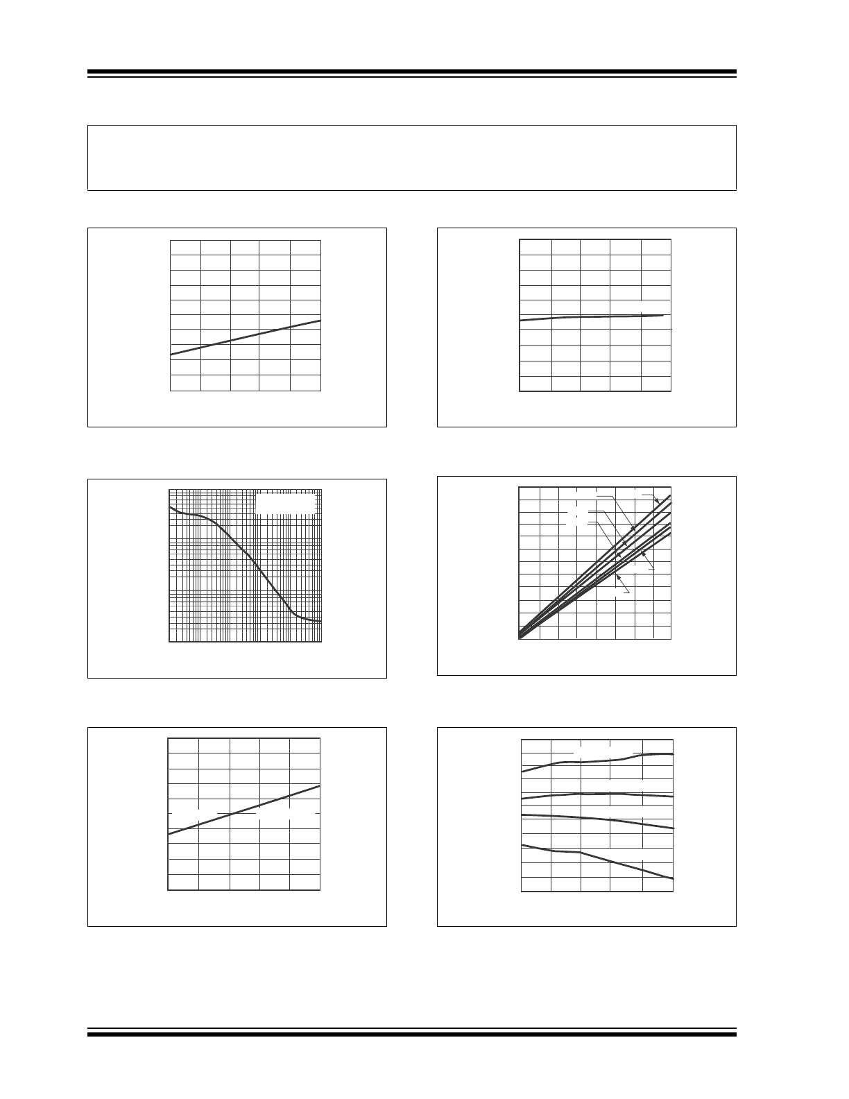
2.0
TYPICAL PERFORMANCE CURVES
FIGURE 2-1:
Line Regulation vs.
Temperature.
FIGURE 2-2:
Output Noise vs. Frequency.
FIGURE 2-3:
Load Regulation vs.
Temperature.
FIGURE 2-4:
I
DD
vs. Temperature.
FIGURE 2-5:
3.0V Dropout Voltage vs.
I
LOAD
.
FIGURE 2-6:
3.0V V
OUT
vs.Temperature.
Note:
The graphs and tables provided following this note are a statistical summary based on a limited number of
samples and are provided for informational purposes only. The performance characteristics listed herein
are not tested or guaranteed. In some graphs or tables, the data presented may be outside the specified
operating range (e.g., outside specified power supply range) and therefore outside the warranted range.
0.020
0.018
0.016
0.012
0.010
0.008
0.006
0.004
0.002
0.000
0.014
TEMPERATURE (°C)
LINE REGULA
TION (%)
-40°C 0°C
25°C 70°C
85°C 125°C
FREQUENCY (kHz)
NOISE (
μ
V/
√
Hz
)
10.0
1.0
0.01
0.01
1
10
100
1000
0.1
0.0
R
LOAD
= 50Ω
C
OUT
= 1
μF
-40°C
0°C
25°C 70°C
85°C 125°C
0.0100
0.0090
0.0080
0.0070
0.0060
0.0050
0.0040
0.0030
0.0020
0.0010
0.0100
TEMPERATURE (°C)
LOAD REGULA
TION (%/mA)
1 mA to 800 mA
V
OUT
= 3V
TEMPERATURE (°C)
I
DD
(
A)
150
135
120
105
90
75
60
45
30
15
0
-40°C 0°C
25°C 70°C
85°C 125°C
V
OUT
= 3V
0.600
0.550
0.500
0.450
0.400
0.350
0.300
0.250
0.200
0.150
0.100
0.050
0.000
0 100 200 300 400 500 600 700 800
ILOAD (mA)
DROPOUT
VOL
TAGE (V)
85°C
125°C
-40°C
0°C
25°C
70°C
3.030
3.020
3.010
3.000
2.990
2.980
2.970
2.960
2.950
2.940
2.930
2.920
TEMPERATURE (°C)
V
OUT
(V)
I
LOAD
= 0.1 mA
I
LOAD
= 300 mA
I
LOAD
= 500 mA
I
LOAD
= 800 mA
-40°C 0°C
25°C 70°C
85°C 125°C
2010 Microchip Technology Inc.
DS21375D-page 5
TC1264
3.0
PIN DESCRIPTIONS
The descriptions of the pins are listed in
Table 3-1
.
TABLE 3-1:
PIN FUNCTION TABLE
3.1
Unregulated Supply (V
IN
)
Unregulated supply input.
3.2
Ground (GND)
Ground terminal.
3.3
Regulated Output Voltage (V
OUT
)
Regulated voltage output.
Pin No.
3-Pin SOT-223
3-Pin TO-220
3-Pin DDPAK
Symbol
Description
1
V
IN
Unregulated supply input
2
GND
Ground terminal
3
V
OUT
Regulated voltage output
TC1264
DS21375D-page 6
2010 Microchip Technology Inc.
4.0
DETAILED DESCRIPTION
The TC1264 is a precision, fixed output LDO. Unlike
bipolar regulators, the TC1264’s supply current does
not increase with load current. In addition, V
OUT
remains stable and within regulation over the entire
0mA to I
LOAD
MAX
load current range (an important
consideration in RTC and CMOS RAM battery back-up
applications).
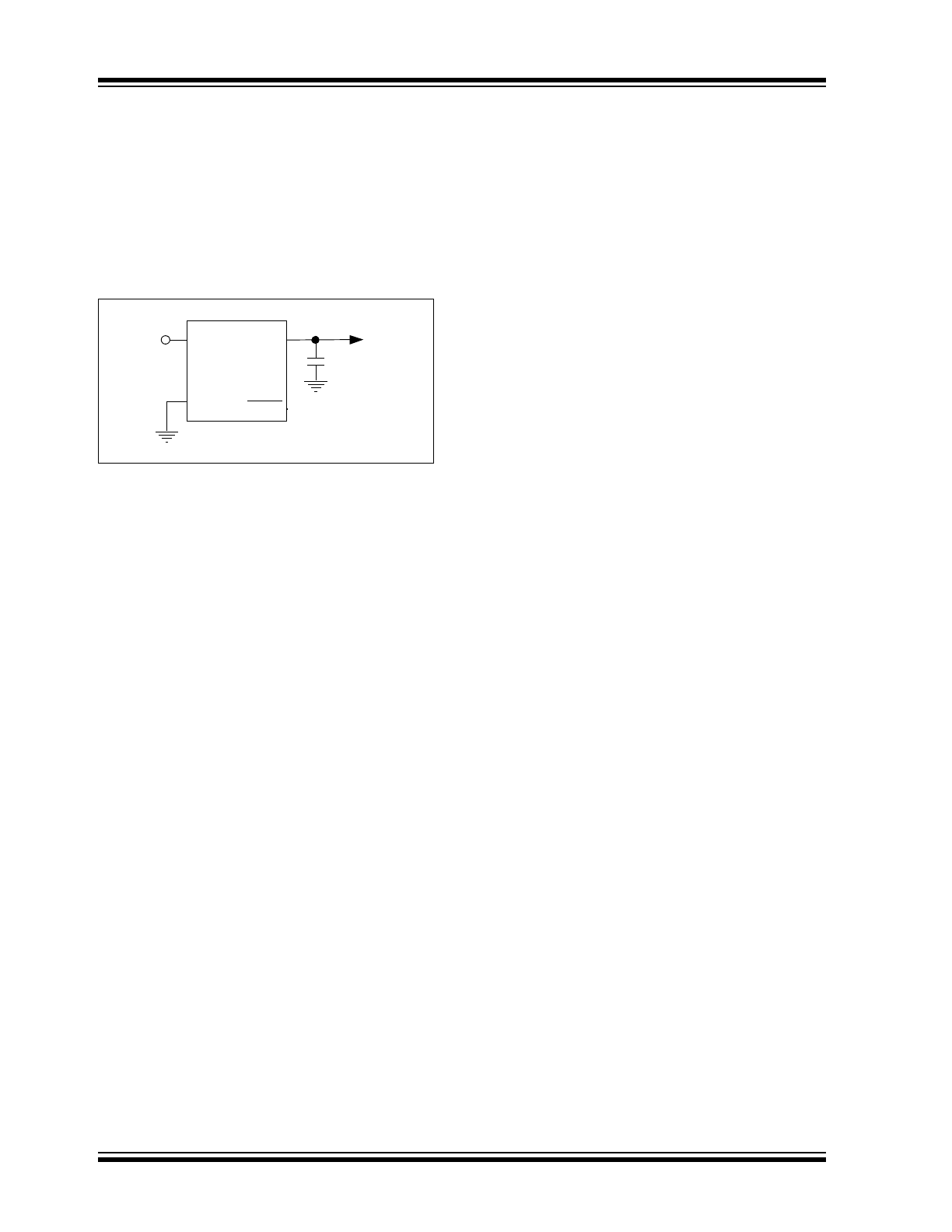
Figure 4-1
shows a typical application circuit.
FIGURE 4-1:
Typical Application Circuit.
4.1
Output Capacitor
A 1 µF (min) capacitor from V
OUT
to ground is required.
The output capacitor should have an effective series
resistance greater than 0.1
and less than 5. A 1 µF
capacitor should be connected from V
IN
to GND if there
is more than 10 inches of wire between the regulator
and the AC filter capacitor, or if a battery is used as the
power source. Aluminum electrolytic or tantalum
capacitor types can be used. (Since many aluminum
electrolytic capacitors freeze at approximately -30°C,
solid tantalums are recommended for applications
operating below -25°C.) When operating from sources
other than batteries, supply-noise rejection and
transient response can be improved by increasing the
value of the input and output capacitors and employing
passive filtering techniques.
TC1264
V
IN
V
OUT
C
1
1 µF
GND
V
OUT
V
IN
SHDN
+
2010 Microchip Technology Inc.
DS21375D-page 7
TC1264
5.0
THERMAL CONSIDERATIONS
5.1
Thermal Shutdown
Integrated thermal protection circuitry shuts the
regulator off when die temperature exceeds 160°C.
The regulator remains off until the die temperature
drops to approximately 150°C.
5.2
Power Dissipation
The amount of power the regulator dissipates is
primarily a function of input and output voltage, and
output current. The following equation is used to
calculate worst-case actual power dissipation:
EQUATION 5-1:
The maximum allowable power dissipation
(
Equation 5-2
) is a function of the maximum ambient
temperature (T
A
MAX
), the maximum allowable die
temperature (T
J
MAX
) and the thermal resistance from
junction-to-air (
JA
).
EQUATION 5-2:
Table 5-1
and
Table 5-2
show various values of
JA
for
the TC1264 packages.
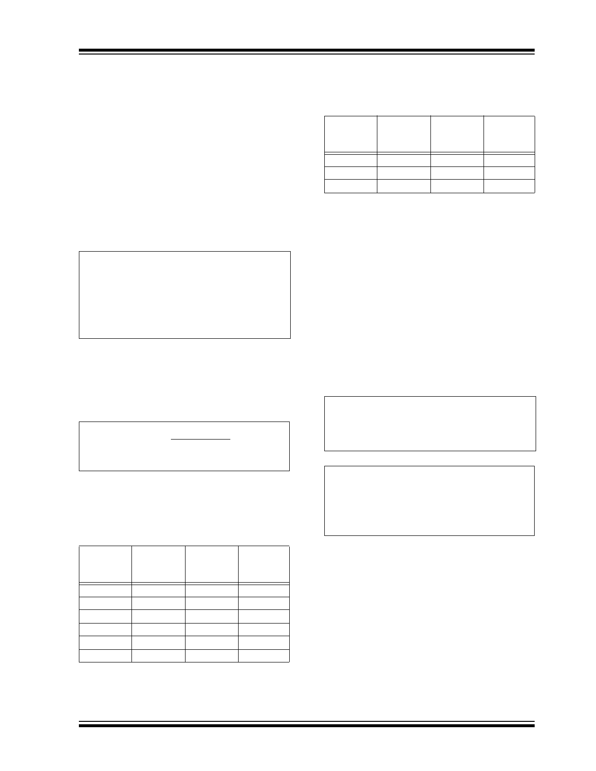
TABLE 5-1:
THERMAL RESISTANCE
GUIDELINES FOR TC1264 IN
SOT-223 PACKAGE
TABLE 5-2:
THERMAL RESISTANCE
GUIDELINES FOR TC1264 IN
3-PIN DDPAK/TO-220
PACKAGE
Equation 5-1
can be used in conjunction with
Equation 5-2
to ensure regulator thermal operation is
within limits. For example:
Find:
1.
Actual power dissipation.
2.
Maximum allowable dissipation.
Actual power dissipation:
Maximum allowable power dissipation:
In this example, the TC1264 dissipates a maximum of
260 mW, which is below the allowable limit of 508 mW.
In a similar manner,
Equation 5-1
and
Equation 5-2
can
be used to calculate maximum current and/or input
voltage limits. For example, the maximum allowable
V
IN
, is found by substituting the maximum allowable
power dissipation of 508 mW into
Equation 5-1
, from
which V
IN
MAX
= 4.6V.
Copper
Area
(Topside)*
Copper
Area
(Backside)
Board
Area
Thermal
Resistance
JA
)
2500 sq mm
2500 sq mm 2500 sq mm
45°C/W
1000 sq mm
2500 sq mm 2500 sq mm
45°C/W
225 sq mm
2500 sq mm 2500 sq mm
53°C/W
100 sq mm
2500 sq mm 2500 sq mm
59°C/W
1000 sq mm
1000 sq mm 1000 sq mm
52°C/W
1000 sq mm
0 sq mm
1000 sq mm
55°C/W
* Tab of device attached to topside copper
Where:
V
INMAX
V
OUTMIN
I
LOADMAX
P
D
= Worst-case actual power dissipation
= Minimum regulator output voltage
= Maximum output (load) current
= Maximum voltage on V
IN
P
D
V
INMAX
V
OUTMIN
–
I
LOADMAX
=
P
D
MAX
= (T
J
MAX
– T
A
MAX
)
JA
Where all terms are previously defined.
Copper
Area
(Topside)*
Copper
Area
(Backside)
Board
Area
Thermal
Resistance
JA
)
2500 sq mm
2500 sq mm 2500 sq mm
25°C/W
1000 sq mm
2500 sq mm 2500 sq mm
27°C/W
125 sq mm
2500 sq mm 2500 sq mm
35°C/W
* Tab of device attached to topside copper
Given:
V
INMAX
= 3.3V ± 10%
V
OUTMIN
= 2.7V ± 0.5%
I
LOADMAX
= 275 mA
T
JMAX
= 125°C
T
AMAX
= 95°C
JA
= 59°C/W (SOT-223)
P
D
V
INMAX
V
OUTMIN
–
I
LOADMAX
P
D
3.3
1.1
2.7
.995
–
275
10
3
–
=
P
D
260 mW
=
P
DMAX
T
JMAX
T
AMAX
–
JA
---------------------------------------
=
P
DMAX
125
95
–
59
-------------------------
=
P
DMAX
508 mW
=
TC1264
DS21375D-page 8
2010 Microchip Technology Inc.
6.0
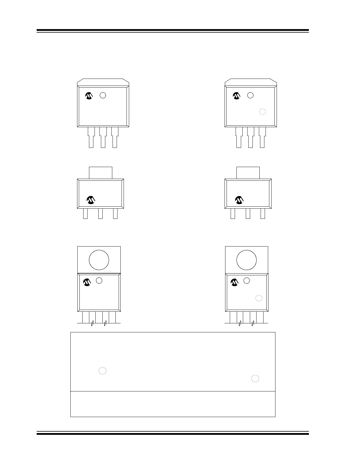
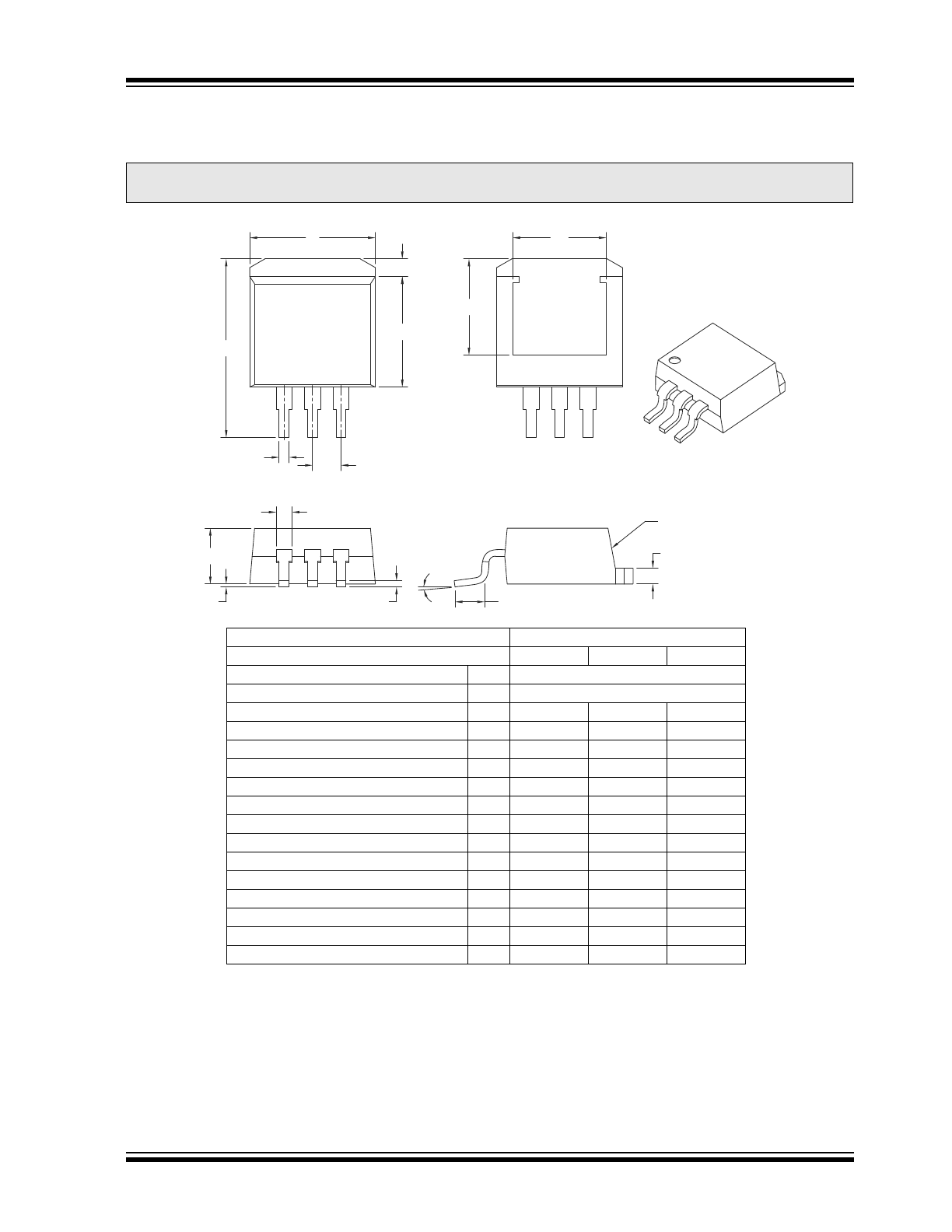
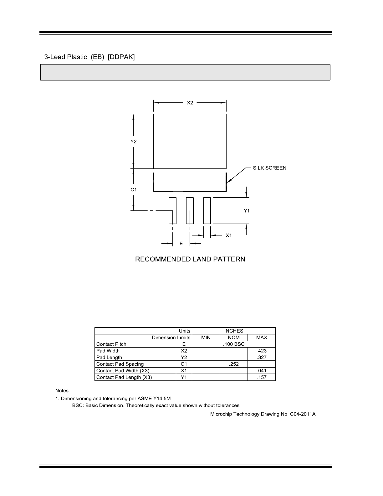
PACKAGING INFORMATION
6.1
Package Marking Information
Legend: XX...X
Customer-specific information
Y
Year code (last digit of calendar year)
YY
Year code (last 2 digits of calendar year)
WW
Week code (week of January 1 is week ‘01’)
NNN
Alphanumeric traceability code
Pb-free JEDEC designator for Matte Tin (Sn)
*
This package is Pb-free. The Pb-free JEDEC designator ( )
can be found on the outer packaging for this package.
Note:
In the event the full Microchip part number cannot be marked on one line, it will
be carried over to the next line, thus limiting the number of available
characters for customer-specific information.
3
e
3
e
XXXXXXXXX
XXXXXXXXX
YYWWNNN
3-Lead DDPAK
Example
3-Lead SOT-223
XXXXXXX
XXXYYWW
NNN
Example
1264-25
VDB1030
256
3-Lead TO-220
XXXXXXXXX
XXXXXXXXX
YYWWNNN
Example
TC1264
3.0VAB^^
1030256
TC1264
1.8VEB^^
1030256
3
e
3
e
2010 Microchip Technology Inc.
DS21375D-page 9
TC1264
/HDG3ODVWLF(%>''3$.@
1RWHV
6LJQLILFDQW&KDUDFWHULVWLF
'LPHQVLRQV'DQG(GRQRWLQFOXGHPROGIODVKRUSURWUXVLRQV0ROGIODVKRUSURWUXVLRQVVKDOOQRWH[FHHGSHUVLGH
'LPHQVLRQLQJDQGWROHUDQFLQJSHU$60(<0
%6& %DVLF'LPHQVLRQ7KHRUHWLFDOO\H[DFWYDOXHVKRZQZLWKRXWWROHUDQFHV
1RWH
)RUWKHPRVWFXUUHQWSDFNDJHGUDZLQJVSOHDVHVHHWKH0LFURFKLS3DFNDJLQJ6SHFLILFDWLRQORFDWHGDW
KWWSZZZPLFURFKLSFRPSDFNDJLQJ
8QLWV
,1&+(6
'LPHQVLRQ/LPLWV
0,1
120
0$;
1XPEHURI3LQV
1
3LWFK
H
%6&
2YHUDOO+HLJKW
$
±
6WDQGRII
$
±
2YHUDOO:LGWK
(
±
([SRVHG3DG:LGWK
(
±
±
0ROGHG3DFNDJH/HQJWK
'
±
2YHUDOO/HQJWK
+
±
([SRVHG3DG/HQJWK
'
±
±
/HDG7KLFNQHVV
F
±
3DG7KLFNQHVV
&
±
/RZHU/HDG:LGWK
E
±
8SSHU/HDG:LGWK
E
±
)RRW/HQJWK
/
±
3DG/HQJWK
/
±
±
)RRW$QJOH
±
E
E1
H
L1
D
D1
N
1
e
b
b1
c
C2
L
A
A1
BOTTOM VIEW
TOP VIEW
CHAMFER
OPTIONAL
φ
0LFURFKLS 7HFKQRORJ\ 'UDZLQJ &%
TC1264
DS21375D-page 10
2010 Microchip Technology Inc.
Note:
For the most current package drawings, please see the Microchip Packaging Specification located at
http://www.microchip.com/packaging