
1997-2012 Microchip Technology Inc.
DS21201K-page 1
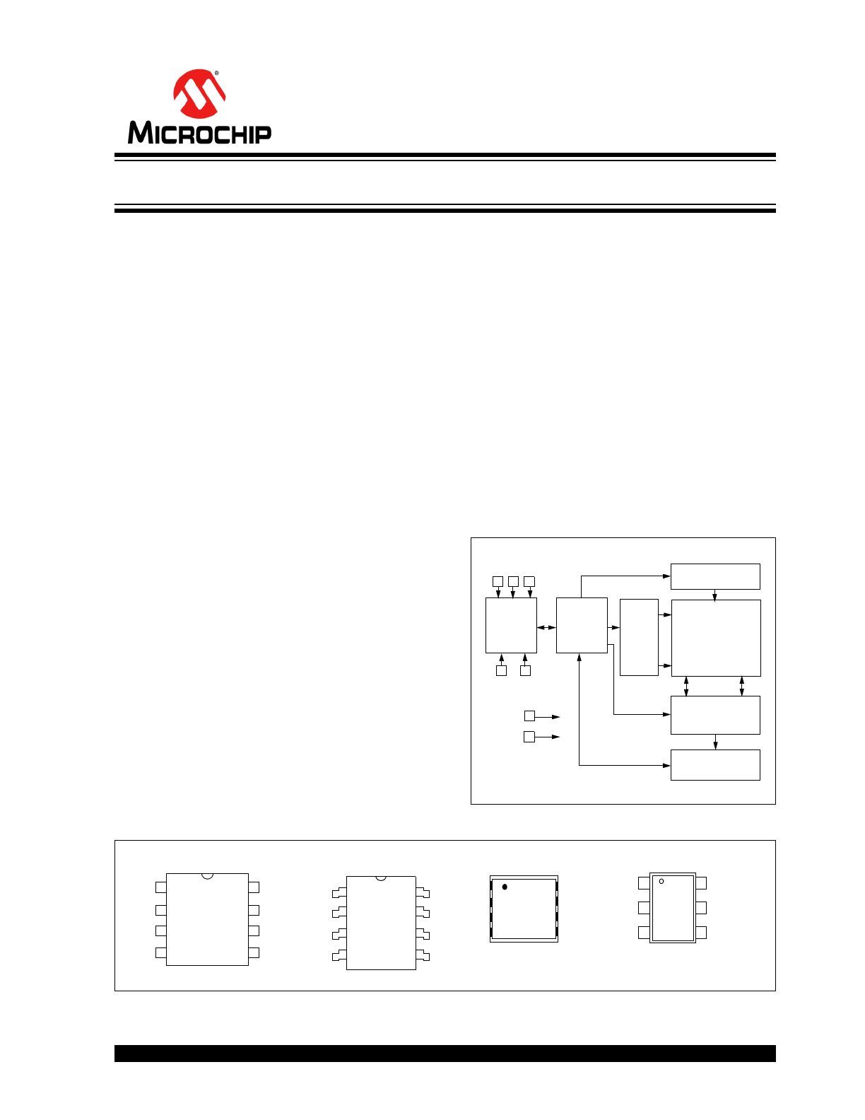
24C01C
Features:
• Single Supply with Operation from 4.5V to 5.5V
• Low-Power CMOS Technology:
- Read current 1 mA, max.
- Standby current 5
A, max.
• 2-Wire Serial Interface, I
2
C™ Compatible
• Cascadable up to Eight Devices
• Schmitt Trigger Inputs for Noise Suppression
• Output Slope Control to Eliminate Ground Bounce
• 100 kHz and 400 kHz Clock Compatibility
• Page Write Time 1 ms max.
• Self-Timed Erase/Write Cycle
• 16-Byte Page Write Buffer
• ESD Protection >4000V
• More than 1 Million Erase/Write Cycles
• Data Retention >200 Years
• Factory Programming Available
• Packages include 8-lead PDIP, SOIC, TSSOP,
DFN, TDFN, MSOP and 6-lead SOT-23
• Pb-Free and RoHS Compliant
• Temperature Ranges:
Description:
The Microchip Technology Inc. 24C01C is a 1K bit
Serial Electrically Erasable PROM with a voltage range
of 4.5V to 5.5V. The device is organized as a single
block of 128 x 8-bit memory with a 2-wire serial
interface. Low-current design permits operation with
max. standby and active currents of only 5
A and 1
mA, respectively. The device has a page write capabil-
ity for up to 16 bytes of data and has fast write cycle
times of only 1 ms for both byte and page writes. Func-
tional address lines allow the connection of up to eight
24C01C devices on the same bus for up to 8K bits of
contiguous EEPROM memory. The device is available
in the standard 8-pin PDIP, 8-pin SOIC (3.90 mm),
8-pin 2x3 DFN and TDFN, 8-pin MSOP and TSSOP
packages. The 24C01C is also available in the 6-lead
SOT-23 package.
Block Diagram
Package Types
- Industrial (I):
-40
C to +85C
- Automotive (E):
-40
C to +125C
I/O
Control
Logic
Memory
Control
Logic
XDEC
HV Generator
EEPROM
Array
YDEC
V
CC
V
SS
Sense Amp.
R/W Control
SDA SCL
A0 A1 A2
A0
A1
A2
V
SS
V
CC
Test
SCL
SDA
1
2
3
4
8
7
6
5
PDIP, MSOP
SOIC, TSSOP
A0
A1
A2
V
SS
1
2
3
4
8
7
6
5
V
CC
Test
SCL
SDA
DFN/TDFN
A0
A1
A2
V
SS
Test
SCL
SDA
V
CC
8
7
6
5
1
2
3
4
SOT-23
V
CC
SCL
SDA
V
SS
A0
A1
1
2
3
4
5
6
1K 5.0V I
2
C™ Serial EEPROM
24C01C
DS21201K-page 2
1997-2012 Microchip Technology Inc.
1.0
ELECTRICAL CHARACTERISTICS
Absolute Maximum Ratings
(†)
V
CC
.............................................................................................................................................................................7.0V
All inputs and outputs w.r.t. V
SS
......................................................................................................... -0.6V to V
CC
+1.0V
Storage temperature ...............................................................................................................................-65°C to +150°C
Ambient temperature with power applied................................................................................................-40°C to +125°C
ESD protection on all pins
4 kV
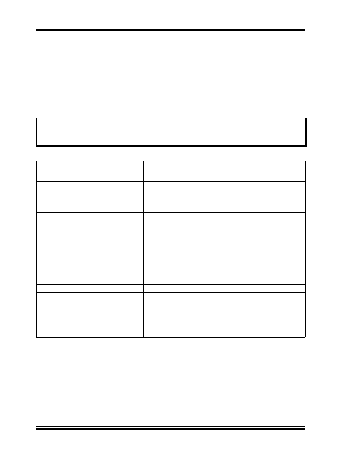
TABLE 1-1:
DC CHARACTERISTICS
† NOTICE: Stresses above those listed under “Absolute Maximum Ratings” may cause permanent damage to the
device. This is a stress rating only and functional operation of the device at these or any other conditions above those
indicated in the operational listings of this specification is not implied. Exposure to Absolute Maximum Rating
conditions for extended periods may affect device reliability.
DC CHARACTERISTICS
Electrical Characteristics:
Industrial (I):
V
CC
= +4.5V to 5.5V
T
A
= -40°C to +85°C
Automotive (E):
V
CC
= +4.5V to 5.5V
T
A
= -40°C to +125°C
Param.
No.
Sym.
Characteristic
Min.
Max.
Units
Conditions
D1
—
A0, A1, A2, SCL, SDA
and WP pins:
—
—
—
—
D2
V
IH
High-level input voltage
0.7 V
CC
—
V
—
D3
V
IL
Low-level input voltage
—
0.3 V
CC
V
—
D4
V
HYS
Hysteresis of Schmitt
Trigger inputs
(SDA, SCL pins)
0.05 V
CC
—
V
(
Note
)
D5
V
OL
Low-level output voltage
—
0.40
V
I
OL
= 3.0 mA @ V
CC
= 4.5V
D6
I
LI
Input leakage current
—
±1
A V
IN
= V
SS
or V
CC
, WP = V
SS
D7
I
LO
Output leakage current
—
±1
A
V
OUT
= V
SS
or V
CC
D8
C
IN
,
C
OUT
Pin capacitance
(all inputs/outputs)
—
10
pF
V
CC
= 5.0V (
Note
)
T
A
= 25°C, f = 1 MHz
D9
I
CC
Read Operating current
—
1
mA
V
CC
= 5.5V, SCL = 400 kHz
I
CC
Write
—
3
mA
V
CC
= 5.5V
D10
I
CCS
Standby current
—
5
A
V
CC
= 5.5V, SDA = SCL = V
CC
WP = V
SS
Note:
This parameter is periodically sampled and not 100% tested.
1997-2012 Microchip Technology Inc.
DS21201K-page 3
24C01C
TABLE 1-2:
AC CHARACTERISTICS
AC CHARACTERISTICS
Electrical Characteristics:
Industrial (I):
V
CC
= +4.5V to 5.5V
T
A
= -40°C to +85°C
Automotive (E):
V
CC
= +4.5V to 5.5V
T
A
= -40°C to +125°C
Param.
No.
Sym.
Characteristic
Min.
Max.
Units
Conditions
1
F
CLK
Clock frequency
—
—
100
400
kHz
—
(I-temp)
2
T
HIGH
Clock high time
4000
600
—
—
ns
—
(I-temp)
3
T
LOW
Clock low time
4700
1300
—
—
ns
—
(I-temp)
4
T
R
SDA and SCL rise time
(
Note 1
)
—
—
1000
300
ns
—
(I-temp)
5
T
F
SDA and SCL fall time
(
Note 1
)
—
300
ns
—
6
T
HD
:
STA
Start condition hold time
4000
600
—
—
ns
—
(I-temp)
7
T
SU
:
STA
Start condition setup time
4700
600
—
—
ns
—
(I-temp)
8
T
HD
:
DAT
Data input hold time
0
—
ns
(
Note 2
)
9
T
SU
:
DAT
Data input setup time
250
100
—
—
ns
—
(I-temp)
10
T
SU
:
STO
Stop condition setup time
4000
600
—
—
ns
—
(I-temp)
11
T
AA
Output valid from clock
(
Note 2
)
—
—
3500
900
ns
—
(I-temp)
12
T
BUF
Bus free time: Time the bus
must be free before a new
transmission can start
4700
1300
—
—
ns
—
(I-temp)
13
T
OF
Output fall time from V
IH
minimum to V
IL
maximum
C
B
100 pF
10 + 0.1CB
250
ns
(
Note 1
)
14
T
SP
Input filter spike suppression
(SDA and SCL pins)
—
50
ns
(
Note 3
)
15
T
WC
Write cycle time (byte or
page)
—
1.5
1
ms
—
(I-temp)
16
—
Endurance
1,000,000
—
cycles 25°C (
Note 4
)
Note 1:
Not 100% tested. C
B
= total capacitance of one bus line in pF.
2:
As a transmitter, the device must provide an internal minimum delay time to bridge the undefined region
(minimum 300 ns) of the falling edge of SCL to avoid unintended generation of Start or Stop conditions.
3:
The combined T
SP
and V
HYS
specifications are due to new Schmitt Trigger inputs, which provide improved
noise spike suppression. This eliminates the need for a T
I
specification for standard operation.
4:
This parameter is not tested but ensured by characterization. For endurance estimates in a specific
application, please consult the Total Endurance™ Model, which can be obtained from Microchip’s web site
at www.microchip.com.
24C01C
DS21201K-page 4
1997-2012 Microchip Technology Inc.
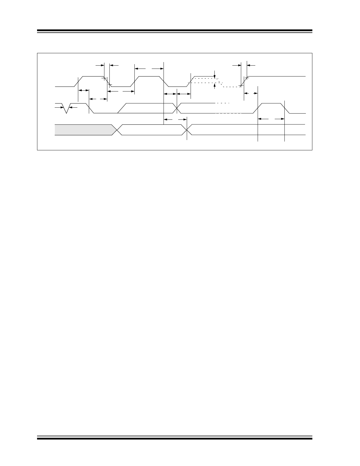
FIGURE 1-1:
BUS TIMING DATA
SCL
SDA
IN
SDA
OUT
5
7
6
14
3
2
8
9
11
D4
4
10
12
1997-2012 Microchip Technology Inc.
DS21201K-page 5
24C01C
2.0
PIN DESCRIPTIONS
The descriptions of the pins are listed in
Table 2-1
.
TABLE 2-1:
PIN FUNCTION TABLE
2.1
SDA Serial Data
This is a bidirectional pin used to transfer addresses
and data into and data out of the device. It is an open
drain terminal; therefore, the SDA bus requires a pull-
up resistor to V
CC
(typical 10 k
for 100 kHz, 2 k for
400 kHz).
For normal data transfer SDA is allowed to change only
during SCL low. Changes during SCL high are
reserved for indicating the Start and Stop conditions.
2.2
SCL Serial Clock
This input is used to synchronize the data transfer from
and to the device.
2.3
A0, A1, A2
The levels on these inputs are compared with the
corresponding bits in the slave address. The chip is
selected if the compare is true.
Up to eight 24C01C devices may be connected to the
same bus by using different Chip Select bit combina-
tions. These inputs must be connected to either V
CC
or
V
SS
.
For the SOT-23 devices up to four devices may be con-
nected to the same bus using different Chip Select bit
combinations.
In most applications, the chip address inputs A0, A1
and A2 are hard-wired to logic ‘0’ or logic ‘1’. For
applications in which these pins are controlled by a
microcontroller or other programmable device, the chip
address pins must be driven to logic ‘0’ or logic ‘1’
before normal device operation can proceed.
2.4
Test
This pin is utilized for testing purposes only. It may be
tied high, tied low or left floating.
2.5
Noise Protection
The 24C01C employs a V
CC
threshold detector circuit
which disables the internal erase/write logic if the V
CC
is below 3.8 volts at nominal conditions.
The SCL and SDA inputs have Schmitt Trigger and
filter circuits which suppress noise spikes to assure
proper device operation even on a noisy bus.
Name
8-pin
PDIP
8-pin
SOIC
8-pin
TSSOP
8-pin
MSOP
8-pin
DFN/TDFN
SOT-23
Function
A0
1
1
1
1
1
5
Chip Select
A1
2
2
2
2
2
4
Chip Select
A2
3
3
3
3
3
—
Chip Select
V
SS
4
4
4
4
4
2
Ground
SDA
5
5
5
5
5
3
Serial Data
SCL
6
6
6
6
6
1
Serial Clock
Test
7
7
7
7
7
—
Test
V
CC
8
8
8
8
8
6
+4.5V to 5.5V Power Supply

24C01C
DS21201K-page 6
1997-2012 Microchip Technology Inc.
3.0
FUNCTIONAL DESCRIPTION
The 24C01C supports a bidirectional 2-wire bus and
data transmission protocol. A device that sends data
onto the bus is defined as transmitter, and a device
receiving data as receiver. The bus has to be controlled
by a master device that generates the Serial Clock
(SCL), controls the bus access, and generates the Start
and Stop conditions, while the 24C01C works as slave.
Both master and slave can operate as transmitter or
receiver, but the master device determines which mode
is activated.
4.0
BUS CHARACTERISTICS
The following bus protocol has been defined:
• Data transfer may be initiated only when the bus
is not busy.
• During data transfer, the data line must remain
stable whenever the clock line is high. Changes in
the data line while the clock line is high will be
interpreted as a Start or Stop condition.
Accordingly, the following bus conditions have been
defined (
Figure 4-1
).
4.1
Bus Not Busy (A)
Both data and clock lines remain high.
4.2
Start Data Transfer (B)
A high-to-low transition of the SDA line while the clock
(SCL) is high determines a Start condition. All
commands must be preceded by a Start condition.
4.3
Stop Data Transfer (C)
A low-to-high transition of the SDA line while the clock
(SCL) is high determines a Stop condition. All
operations must be ended with a Stop condition.
4.4
Data Valid (D)
The state of the data line represents valid data when,
after a Start condition, the data line is stable for the
duration of the high period of the clock signal.
The data on the line must be changed during the low
period of the clock signal. There is one bit of data per
clock pulse.
Each data transfer is initiated with a Start condition and
terminated with a Stop condition. The number of the
data bytes transferred between the Start and Stop
conditions is determined by the master device and is
theoretically unlimited, although only the last sixteen
will be stored when doing a write operation. When an
overwrite does occur it will replace data in a first-in first-
out fashion.
4.5
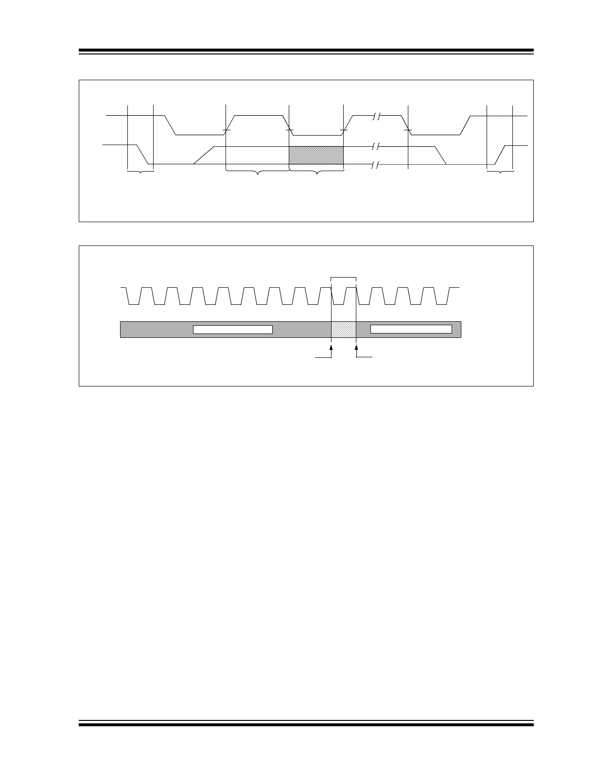
Acknowledge
Each receiving device, when addressed, is required to
generate an acknowledge after the reception of each
byte. The master device must generate an extra clock
pulse, which is associated with this Acknowledge bit.
The device that acknowledges has to pull down the
SDA line during the Acknowledge clock pulse in such a
way that the SDA line is stable low during the high
period of the acknowledge related clock pulse. Of
course, setup and hold times must be taken into
account. A master must signal an end of data to the
slave by not generating an Acknowledge bit on the last
byte that has been clocked out of the slave. In this case,
the slave must leave the data line high to enable the
master to generate the Stop condition (
Figure 4-2
)
Note:
The 24C01C does not generate any
Acknowledge bits if an internal program-
ming cycle is in progress.
1997-2012 Microchip Technology Inc.
DS21201K-page 7
24C01C
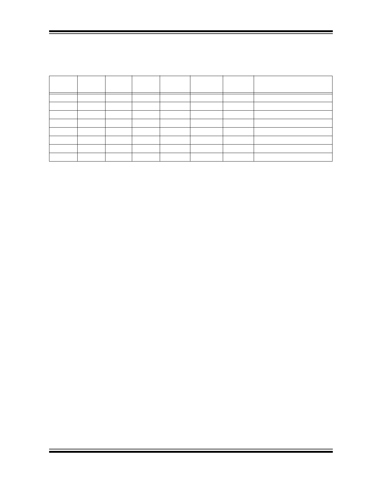
FIGURE 4-1:
DATA TRANSFER SEQUENCE ON THE SERIAL BUS
FIGURE 4-2:
ACKNOWLEDGE TIMING
(A)
(B)
(C)
(D)
(A)
(C)
SCL
SDA
Start
Condition
Address or
Acknowledge
Valid
Data
Allowed
to Change
Stop
Condition
SCL
9
8
7
6
5
4
3
2
1
1
2
3
Transmitter must release the SDA line at this point
allowing the Receiver to pull the SDA line low to
acknowledge the previous eight bits of data.
Receiver must release the SDA line at this
point so the Transmitter can continue send-
ing data.
Data from transmitter
Data from transmitter
SDA
Acknowledge
Bit
24C01C
DS21201K-page 8
1997-2012 Microchip Technology Inc.
5.0
DEVICE ADDRESSING
A control byte is the first byte received following the
Start condition from the master device (
Figure 5-1
).
The control byte consists of a four-bit control code; for
the 24C01C this is set as ‘1010’ binary for read and
write operations. The next three bits of the control byte
are the Chip Select bits (A2, A1, A0). The Chip Select
bits allow the use of up to eight 24C01C devices on the
same bus and are used to select which device is
accessed. The Chip Select bits in the control byte must
correspond to the logic levels on the corresponding A2,
A1 and A0 pins for the device to respond. These bits
are in effect the three Most Significant bits of the word
address.
For the SOT-23 package, the A2 address pin is not
available. During device addressing, the A2 Chip
Select bit should be set to ‘0’.
The last bit of the control byte defines the operation to
be performed. When set to a ‘1’ a read operation is
selected, and when set to a ‘0’ a write operation is
selected. Following the Start condition, the 24C01C
monitors the SDA bus checking the control byte being
transmitted. Upon receiving a ‘1010’ code and appro-
priate Chip Select bits, the slave device outputs an
Acknowledge signal on the SDA line. Depending on the
state of the R/W bit, the 24C01C will select a read or
write operation.
FIGURE 5-1:
CONTROL BYTE
FORMAT
5.1
Contiguous Addressing Across
Multiple Devices
The Chip Select bits A2, A1, A0 can be used to expand
the contiguous address space for up to 8K bits by
adding up to eight 24C01C devices on the same bus.
In this case, software can use A0 of the control byte as
address bit A8, A1 as address bit A9, and A2 as
address bit A10. It is not possible to sequentially read
across device boundaries.
For the SOT-23 package, up to four 24C01C devices
can be added for up to 4K bits of address space. In this
case, software can use A0 of the control byte as
address bit A8, and A1 as address bit A9. It is not pos-
sible to sequentially read across device boundaries.
1
0
1
0
A2 A1 A0
S
ACK
R/W
Control Code
Chip Select
Bits
Slave Address
Acknowledge Bit
Start Bit
Read/Write Bit
1997-2012 Microchip Technology Inc.
DS21201K-page 9
24C01C
6.0
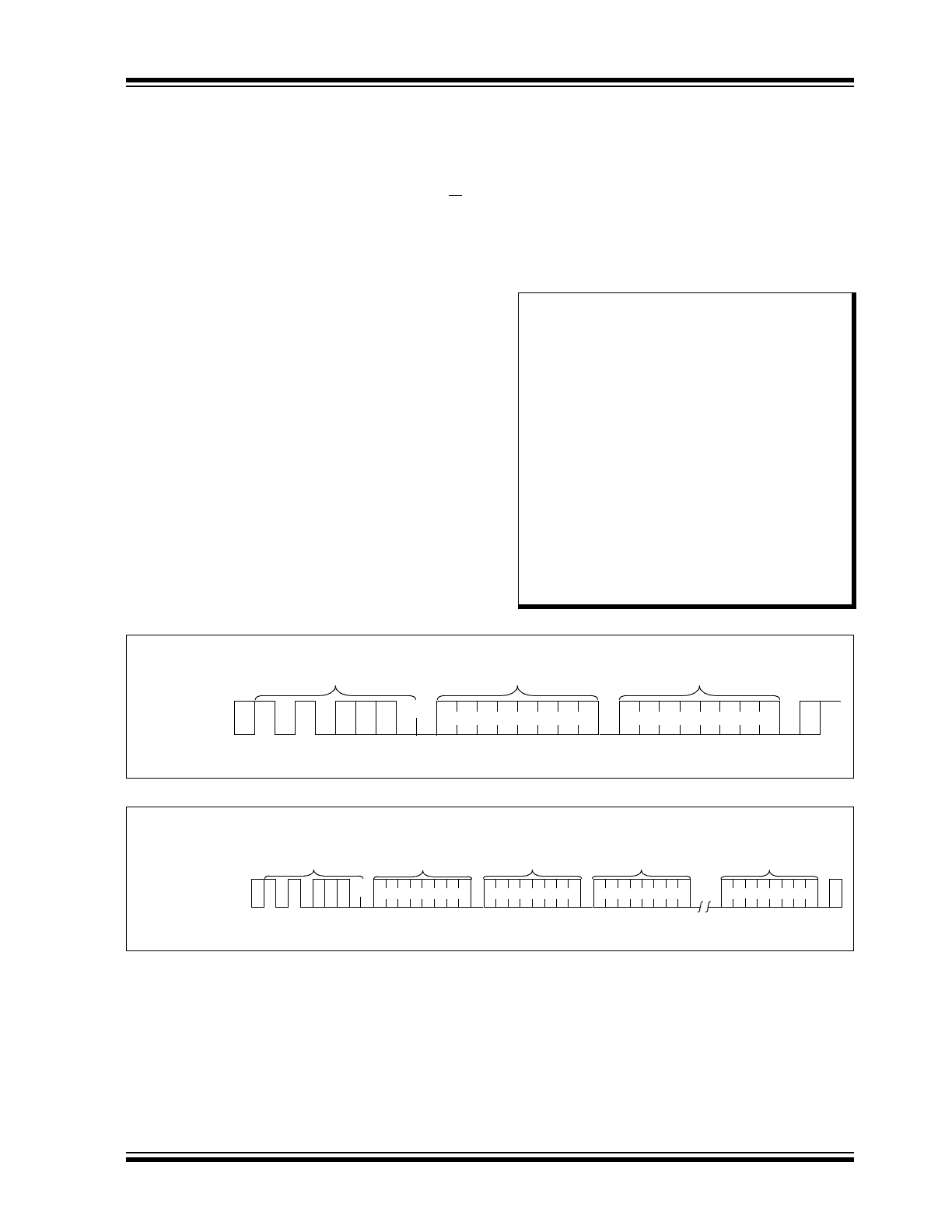
WRITE OPERATIONS
6.1
Byte Write
Following the Start signal from the master, the device
code (4 bits), the Chip Select bits (3 bits), and the R/W
bit, which is a logic low, is placed onto the bus by the
master transmitter. The device will acknowledge this
control byte during the ninth clock pulse. The next byte
transmitted by the master is the word address and will
be written into the Address Pointer of the 24C01C.
After receiving another Acknowledge signal from the
24C01C the master device will transmit the data word
to be written into the addressed memory location. The
24C01C acknowledges again and the master gener-
ates a Stop condition. This initiates the internal write
cycle, and during this time the 24C01C will not
generate Acknowledge signals (
Figure 6-1
).
6.2
Page Write
The write control byte, word address and the first data
byte are transmitted to the 24C01C in the same way as
in a byte write. But instead of generating a Stop
condition, the master transmits up to 15 additional data
bytes to the 24C01C which are temporarily stored in
the on-chip page buffer and will be written into the
memory after the master has transmitted a Stop
condition.
After the receipt of each word, the four lower order
Address Pointer bits are internally incremented by one.
The higher order four bits of the word address remains
constant. If the master should transmit more than 16
bytes prior to generating the Stop condition, the
address counter will roll over and the previously
received data will be overwritten. As with the byte write
operation, once the Stop condition is received an
internal write cycle will begin (
Figure 6-2
).
FIGURE 6-1:
BYTE WRITE
FIGURE 6-2:
PAGE WRITE
Note:
Page write operations are limited to writ-
ing bytes within a single physical page,
regardless of the number of bytes actu-
ally being written. Physical page boundar-
ies start at addresses that are integer
multiples of the page buffer size (or ‘page
size’) and end at addresses that are
integer multiples of [page size – 1]. If a
Page Write command attempts to write
across a physical page boundary, the
result is that the data wraps around to the
beginning of the current page (overwriting
data previously stored there), instead of
being written to the next page as might be
expected. It is therefore necessary for the
application software to prevent page write
operations that would attempt to cross a
page boundary.
S
P
Bus Activity
Master
SDA Line
Bus Activity
S
T
A
R
T
S
T
O
P
Control
Byte
Word
Address
Data
A
C
K
A
C
K
A
C
K
S
P
Bus Activity
Master
SDA Line
Bus Activity
S
T
A
R
T
Control
Byte
Word
Address (n)
Data n
Data n + 15
S
T
O
P
A
C
K
A
C
K
A
C
K
A
C
K
A
C
K
Data n +1
24C01C
DS21201K-page 10
1997-2012 Microchip Technology Inc.
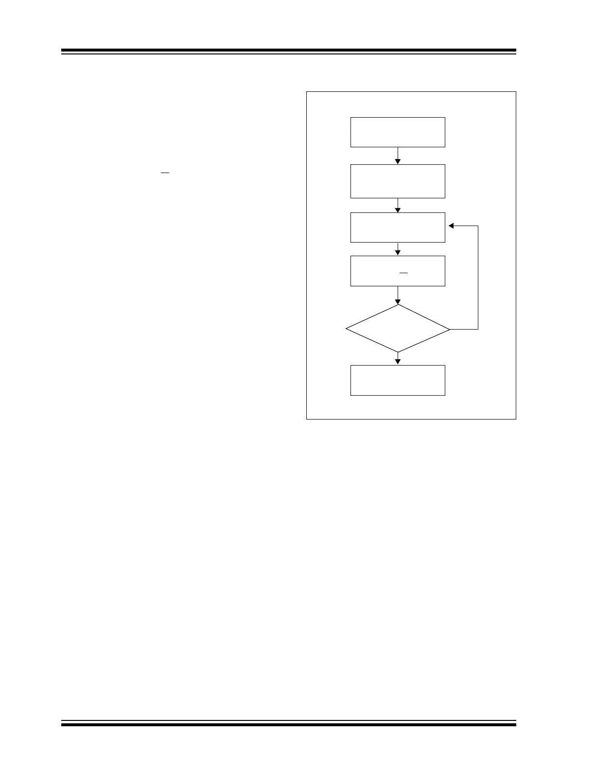
7.0
ACKNOWLEDGE POLLING
Since the device will not acknowledge during a write
cycle, this can be used to determine when the cycle is
complete (this feature can be used to maximize bus
throughput). Once the Stop condition for a Write
command has been issued from the master, the device
initiates the internally timed write cycle. ACK polling
can be initiated immediately. This involves the master
sending a Start condition followed by the control byte
for a Write command (R/W = 0). If the device is still
busy with the write cycle, then no ACK will be returned.
If no ACK is returned, then the Start bit and control byte
must be re-sent. If the cycle is complete, then the
device will return the ACK and the master can then
proceed with the next Read or Write command. See
Figure 7-1
for flow diagram.
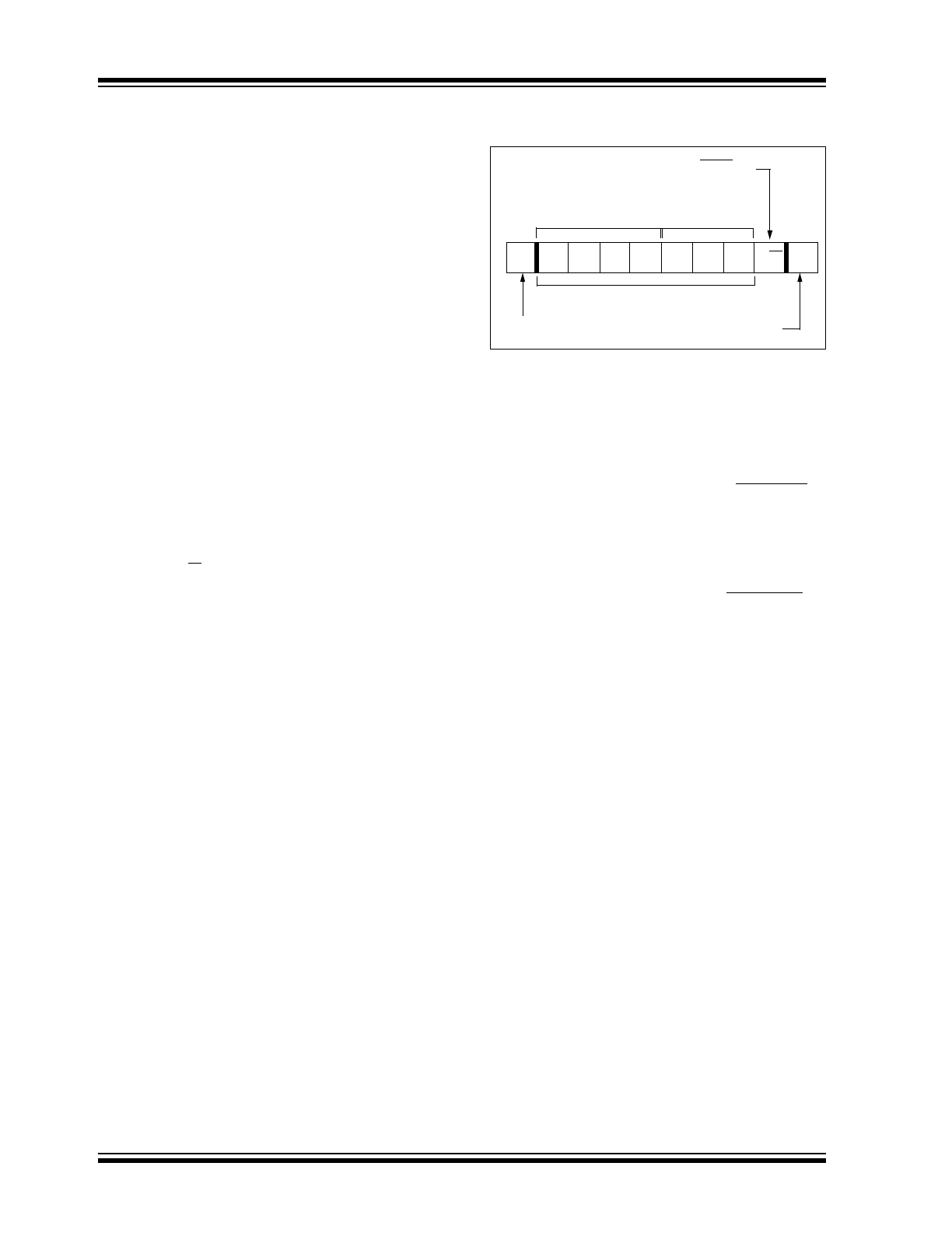
FIGURE 7-1:
ACKNOWLEDGE
POLLING FLOW
Send
Write Command
Send Stop
Condition to
Initiate Write Cycle
Send Start
Send Control Byte
with R/W = 0
Did Device
Acknowledge
(ACK = 0)?
Next
Operation
NO
YES