
Features
•
High-performance, Low-power Atmel
®
AVR
®
8-bit Microcontroller
•
Advanced RISC Architecture
– 131 Powerful Instructions – Most Single-clock Cycle Execution
– 32 × 8 General Purpose Working Registers
– Fully Static Operation
– Up to 16 MIPS Throughput at 16 MHz
– On-chip 2-cycle Multiplier
•
High Endurance Non-volatile Memory segments
– 16 Kbytes of In-System Self-programmable Flash program memory
– 512 Bytes EEPROM
– 1 Kbyte Internal SRAM
– Write/Erase Cycles: 10,000 Flash/100,000 EEPROM
– Data retention: 20 years at 85°C/100 years at 25°C
(1)
– Optional Boot Code Section with Independent Lock Bits
In-System Programming by On-chip Boot Program
True Read-While-Write Operation
– Programming Lock for Software Security
•
JTAG (IEEE std. 1149.1 Compliant) Interface
– Boundary-scan Capabilities According to the JTAG Standard
– Extensive On-chip Debug Support
– Programming of Flash, EEPROM, Fuses, and Lock Bits through the JTAG Interface
•
Peripheral Features
– Two 8-bit Timer/Counters with Separate Prescalers and Compare Modes
– One 16-bit Timer/Counter with Separate Prescaler, Compare Mode, and Capture
Mode
– Real Time Counter with Separate Oscillator
– Four PWM Channels
– 8-channel, 10-bit ADC
8 Single-ended Channels
7 Differential Channels in TQFP Package Only
2 Differential Channels with Programmable Gain at 1x, 10x, or 200x
– Byte-oriented Two-wire Serial Interface
– Programmable Serial USART
– Master/Slave SPI Serial Interface
– Programmable Watchdog Timer with Separate On-chip Oscillator
– On-chip Analog Comparator
•
Special Microcontroller Features
– Power-on Reset and Programmable Brown-out Detection
– Internal Calibrated RC Oscillator
– External and Internal Interrupt Sources
– Six Sleep Modes: Idle, ADC Noise Reduction, Power-save, Power-down, Standby
and Extended Standby
•
I/O and Packages
– 32 Programmable I/O Lines
– 40-pin PDIP, 44-lead TQFP, and 44-pad QFN/MLF
•
Operating Voltages
– 2.7V - 5.5V for ATmega16L
– 4.5V - 5.5V for ATmega16
•
Speed Grades
– 0 - 8 MHz for ATmega16L
– 0 - 16 MHz for ATmega16
•
Power Consumption @ 1 MHz, 3V, and 25
°
C for ATmega16L
– Active: 1.1 mA
– Idle Mode: 0.35 mA
– Power-down Mode: < 1 µA
8-bit
Microcontroller
with 16K Bytes
In-System
Programmable
Flash
ATmega16
ATmega16L
Summary
Rev. 2466TS–AVR–07/10
2
2466TS–AVR–07/10
ATmega16(L)
Pin
Configurations
Figure 1. Pinout ATmega16
Disclaimer
Typical values contained in this datasheet are based on simulations and characterization of
other AVR microcontrollers manufactured on the same process technology. Min and Max values
will be available after the device is characterized.
(XCK/T0) PB0
(T1) PB1
(INT2/AIN0) PB2
(OC0/AIN1) PB3
(SS) PB4
(MOSI) PB5
(MISO) PB6
(SCK) PB7
RESET
VCC
GND
XTAL2
XTAL1
(RXD) PD0
(TXD) PD1
(INT0) PD2
(INT1) PD3
(OC1B) PD4
(OC1A) PD5
(ICP1) PD6
PA0 (ADC0)
PA1 (ADC1)
PA2 (ADC2)
PA3 (ADC3)
PA4 (ADC4)
PA5 (ADC5)
PA6 (ADC6)
PA7 (ADC7)
AREF
GND
AVCC
PC7 (TOSC2)
PC6 (TOSC1)
PC5 (TDI)
PC4 (TDO)
PC3 (TMS)
PC2 (TCK)
PC1 (SDA)
PC0 (SCL)
PD7 (OC2)
PA4 (ADC4)
PA5 (ADC5)
PA6 (ADC6)
PA7 (ADC7)
AREF
GND
AVCC
PC7 (TOSC2)
PC6 (TOSC1)
PC5 (TDI)
PC4 (TDO)
(MOSI) PB5
(MISO) PB6
(SCK) PB7
RESET
VCC
GND
XTAL2
XTAL1
(RXD) PD0
(TXD) PD1
(INT0) PD2
(INT1) PD3 (OC1B) PD4 (OC1A) PD5 (ICP1) PD6 (OC2) PD7
VCC GND
(SCL) PC0 (SDA) PC1 (TCK) PC2 (TMS) PC3
PB4 (SS) PB3 (AIN1/OC0) PB2 (AIN0/INT2) PB1 (T1) PB0 (XCK/T0) GND VCC PA
0 (ADC0)
PA
1 (ADC1)
PA
2 (ADC2)
PA
3 (ADC3)
PDIP
TQFP/QFN/MLF
NOTE:
Bottom pad should
be soldered to ground.
3
2466TS–AVR–07/10
ATmega16(L)
Overview
The ATmega16 is a low-power CMOS 8-bit microcontroller based on the AVR enhanced RISC
architecture. By executing powerful instructions in a single clock cycle, the ATmega16 achieves
throughputs approaching 1 MIPS per MHz allowing the system designer to optimize power con-
sumption versus processing speed.
Block Diagram
Figure 2. Block Diagram
INTERNAL
OSCILLATOR
OSCILLATOR
WATCHDOG
TIMER
MCU CTRL.
& TIMING
OSCILLATOR
TIMERS/
COUNTERS
INTERRUPT
UNIT
STACK
POINTER
EEPROM
SRAM
STATUS
REGISTER
USART
PROGRAM
COUNTER
PROGRAM
FLASH
INSTRUCTION
REGISTER
INSTRUCTION
DECODER
PROGRAMMING
LOGIC
SPI
ADC
INTERFACE
COMP.
INTERFACE
PORTA DRIVERS/BUFFERS
PORTA DIGITAL INTERFACE
GENERAL
PURPOSE
REGISTERS
X
Y
Z
ALU
+
-
PORTC DRIVERS/BUFFERS
PORTC DIGITAL INTERFACE
PORTB DIGITAL INTERFACE
PORTB DRIVERS/BUFFERS
PORTD DIGITAL INTERFACE
PORTD DRIVERS/BUFFERS
XTAL1
XTAL2
RESET
CONTROL
LINES
VCC
GND
MUX &
ADC
AREF
PA0 - PA7
PC0 - PC7
PD0 - PD7
PB0 - PB7
AVR CPU
TWI
AVCC
INTERNAL
CALIBRATED
OSCILLATOR

4
2466TS–AVR–07/10
ATmega16(L)
The AVR core combines a rich instruction set with 32 general purpose working registers. All the
32 registers are directly connected to the Arithmetic Logic Unit (ALU), allowing two independent
registers to be accessed in one single instruction executed in one clock cycle. The resulting
architecture is more code efficient while achieving throughputs up to ten times faster than con-
ventional CISC microcontrollers.
The ATmega16 provides the following features: 16 Kbytes of In-System Programmable Flash
Program memory with Read-While-Write capabilities, 512 bytes EEPROM, 1 Kbyte SRAM, 32
general purpose I/O lines, 32 general purpose working registers, a JTAG interface for Boundary-
scan, On-chip Debugging support and programming, three flexible Timer/Counters with com-
pare modes, Internal and External Interrupts, a serial programmable USART, a byte oriented
Two-wire Serial Interface, an 8-channel, 10-bit ADC with optional differential input stage with
programmable gain (TQFP package only), a programmable Watchdog Timer with Internal Oscil-
lator, an SPI serial port, and six software selectable power saving modes. The Idle mode stops
the CPU while allowing the USART, Two-wire interface, A/D Converter, SRAM, Timer/Counters,
SPI port, and interrupt system to continue functioning. The Power-down mode saves the register
contents but freezes the Oscillator, disabling all other chip functions until the next External Inter-
rupt or Hardware Reset. In Power-save mode, the Asynchronous Timer continues to run,
allowing the user to maintain a timer base while the rest of the device is sleeping. The ADC
Noise Reduction mode stops the CPU and all I/O modules except Asynchronous Timer and
ADC, to minimize switching noise during ADC conversions. In Standby mode, the crystal/reso-
nator Oscillator is running while the rest of the device is sleeping. This allows very fast start-up
combined with low-power consumption. In Extended Standby mode, both the main Oscillator
and the Asynchronous Timer continue to run.
The device is manufactured using Atmel’s high density nonvolatile memory technology. The On-
chip ISP Flash allows the program memory to be reprogrammed in-system through an SPI serial
interface, by a conventional nonvolatile memory programmer, or by an On-chip Boot program
running on the AVR core. The boot program can use any interface to download the application
program in the Application Flash memory. Software in the Boot Flash section will continue to run
while the Application Flash section is updated, providing true Read-While-Write operation. By
combining an 8-bit RISC CPU with In-System Self-Programmable Flash on a monolithic chip,
the Atmel ATmega16 is a powerful microcontroller that provides a highly-flexible and cost-effec-
tive solution to many embedded control applications.
The ATmega16 AVR is supported with a full suite of program and system development tools
including: C compilers, macro assemblers, program debugger/simulators, in-circuit emulators,
and evaluation kits.
Pin Descriptions
VCC
Digital supply voltage.
GND
Ground.
Port A (PA7..PA0)
Port A serves as the analog inputs to the A/D Converter.
Port A also serves as an 8-bit bi-directional I/O port, if the A/D Converter is not used. Port pins
can provide internal pull-up resistors (selected for each bit). The Port A output buffers have sym-
metrical drive characteristics with both high sink and source capability. When pins PA0 to PA7
are used as inputs and are externally pulled low, they will source current if the internal pull-up
resistors are activated. The Port A pins are tri-stated when a reset condition becomes active,
even if the clock is not running.

5
2466TS–AVR–07/10
ATmega16(L)
Port B (PB7..PB0)
Port B is an 8-bit bi-directional I/O port with internal pull-up resistors (selected for each bit). The
Port B output buffers have symmetrical drive characteristics with both high sink and source
capability. As inputs, Port B pins that are externally pulled low will source current if the pull-up
resistors are activated. The Port B pins are tri-stated when a reset condition becomes active,
even if the clock is not running.
Port B also serves the functions of various special features of the ATmega16 as listed on
page
58
.
Port C (PC7..PC0)
Port C is an 8-bit bi-directional I/O port with internal pull-up resistors (selected for each bit). The
Port C output buffers have symmetrical drive characteristics with both high sink and source
capability. As inputs, Port C pins that are externally pulled low will source current if the pull-up
resistors are activated. The Port C pins are tri-stated when a reset condition becomes active,
even if the clock is not running. If the JTAG interface is enabled, the pull-up resistors on pins
PC5(TDI), PC3(TMS) and PC2(TCK) will be activated even if a reset occurs.
Port C also serves the functions of the JTAG interface and other special features of the
ATmega16 as listed on
page 61
.
Port D (PD7..PD0)
Port D is an 8-bit bi-directional I/O port with internal pull-up resistors (selected for each bit). The
Port D output buffers have symmetrical drive characteristics with both high sink and source
capability. As inputs, Port D pins that are externally pulled low will source current if the pull-up
resistors are activated. The Port D pins are tri-stated when a reset condition becomes active,
even if the clock is not running.
Port D also serves the functions of various special features of the ATmega16 as listed on
page
63
.
RESET
Reset Input. A low level on this pin for longer than the minimum pulse length will generate a
reset, even if the clock is not running. The minimum pulse length is given in
Table 15 on page
38
. Shorter pulses are not guaranteed to generate a reset.
XTAL1
Input to the inverting Oscillator amplifier and input to the internal clock operating circuit.
XTAL2
Output from the inverting Oscillator amplifier.
AVCC
AVCC is the supply voltage pin for Port A and the A/D Converter. It should be externally con-
nected to V
CC
, even if the ADC is not used. If the ADC is used, it should be connected to V
CC
through a low-pass filter.
AREF
AREF is the analog reference pin for the A/D Converter.

6
2466TS–AVR–07/10
ATmega16(L)
Resources
A comprehensive set of development tools, application notes and datasheets are available for
download on http://www.atmel.com/avr.
Note:
1.
Data Retention
Reliability Qualification results show that the projected data retention failure rate is much less
than 1 PPM over 20 years at 85°C or 100 years at 25°C.
7
2466TS–AVR–07/10
ATmega16(L)
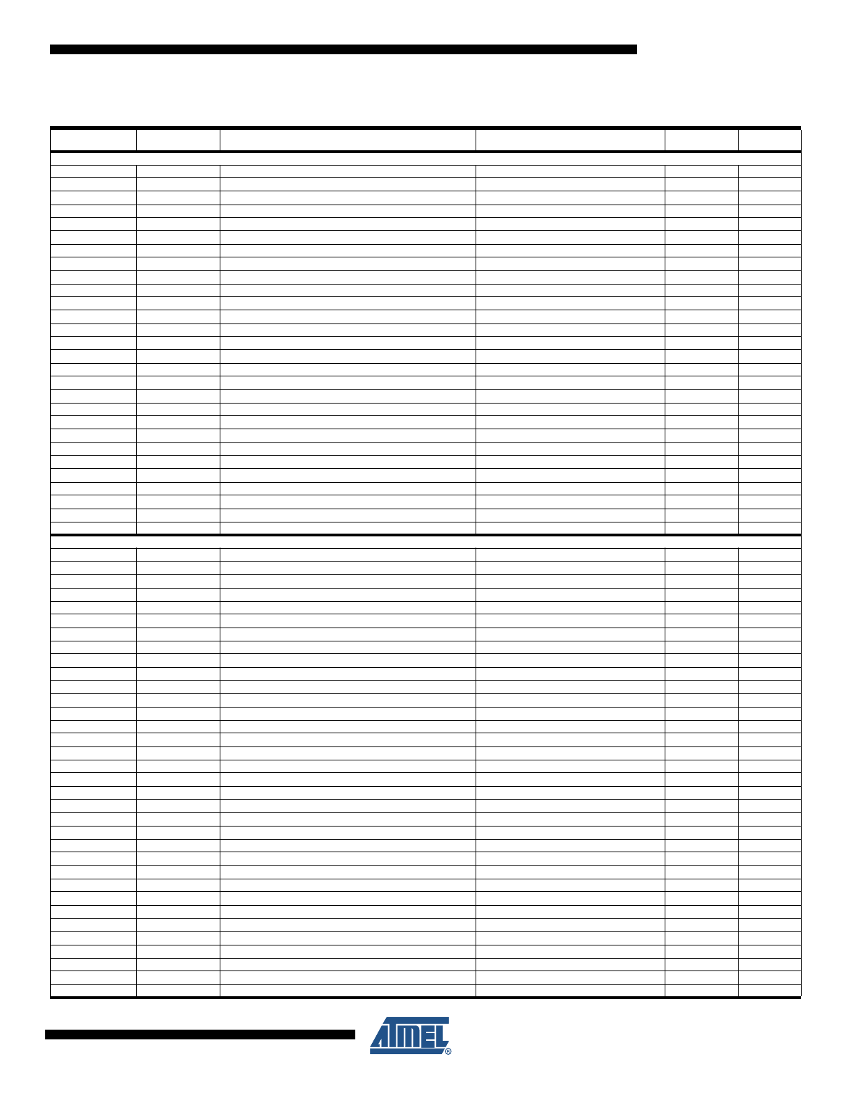
Register Summary
Address
Name
Bit 7
Bit 6
Bit 5
Bit 4
Bit 3
Bit 2
Bit 1
Bit 0
Page
$3F ($5F)
SREG
I
T
H
S
V
N
Z
C
9
$3E ($5E)
SPH
–
–
–
–
–
SP10
SP9
SP8
12
$3D ($5D)
SPL
SP7
SP6
SP5
SP4
SP3
SP2
SP1
SP0
12
$3C ($5C)
OCR0
Timer/Counter0 Output Compare Register
85
$3B ($5B)
GICR
INT1
INT0
INT2
–
–
–
IVSEL
IVCE
48, 69
$3A ($5A)
GIFR
INTF1
INTF0
INTF2
–
–
–
–
–
70
$39 ($59)
TIMSK
OCIE2
TOIE2
TICIE1
OCIE1A
OCIE1B
TOIE1
OCIE0
TOIE0
85, 115, 133
$38 ($58)
TIFR
OCF2
TOV2
ICF1
OCF1A
OCF1B
TOV1
OCF0
TOV0
86, 115, 133
$37 ($57)
SPMCR
SPMIE
RWWSB
–
RWWSRE
BLBSET
PGWRT
PGERS
SPMEN
250
$36 ($56)
TWCR
TWINT
TWEA
TWSTA
TWSTO
TWWC
TWEN
–
TWIE
180
$35 ($55)
MCUCR
SM2
SE
SM1
SM0
ISC11
ISC10
ISC01
ISC00
32, 68
$34 ($54)
MCUCSR
JTD
ISC2
–
JTRF
WDRF
BORF
EXTRF
PORF
41, 69, 231
$33 ($53)
TCCR0
FOC0
WGM00
COM01
COM00
WGM01
CS02
CS01
CS00
83
$32 ($52)
TCNT0
Timer/Counter0 (8 Bits)
85
$31
(1)
($51)
(1)
OSCCAL
Oscillator Calibration Register
30
OCDR
On-Chip Debug Register
227
$30 ($50)
SFIOR
ADTS2
ADTS1
ADTS0
–
ACME
PUD
PSR2
PSR10
57,88,134,201,221
$2F ($4F)
TCCR1A
COM1A1
COM1A0
COM1B1
COM1B0
FOC1A
FOC1B
WGM11
WGM10
110
$2E ($4E)
TCCR1B
ICNC1
ICES1
–
WGM13
WGM12
CS12
CS11
CS10
113
$2D ($4D)
TCNT1H
Timer/Counter1 – Counter Register High Byte
114
$2C ($4C)
TCNT1L
Timer/Counter1 – Counter Register Low Byte
114
$2B ($4B)
OCR1AH
Timer/Counter1 – Output Compare Register A High Byte
114
$2A ($4A)
OCR1AL
Timer/Counter1 – Output Compare Register A Low Byte
114
$29 ($49)
OCR1BH
Timer/Counter1 – Output Compare Register B High Byte
114
$28 ($48)
OCR1BL
Timer/Counter1 – Output Compare Register B Low Byte
114
$27 ($47)
ICR1H
Timer/Counter1 – Input Capture Register High Byte
114
$26 ($46)
ICR1L
Timer/Counter1 – Input Capture Register Low Byte
114
$25 ($45)
TCCR2
FOC2
WGM20
COM21
COM20
WGM21
CS22
CS21
CS20
128
$24 ($44)
TCNT2
Timer/Counter2 (8 Bits)
130
$23 ($43)
OCR2
Timer/Counter2 Output Compare Register
130
$22 ($42)
ASSR
–
–
–
–
AS2
TCN2UB
OCR2UB
TCR2UB
131
$21 ($41)
WDTCR
–
–
–
WDTOE
WDE
WDP2
WDP1
WDP0
43
$20
(2)
($40)
(2)
UBRRH
URSEL
–
–
–
UBRR[11:8]
167
UCSRC
URSEL
UMSEL
UPM1
UPM0
USBS
UCSZ1
UCSZ0
UCPOL
166
$1F ($3F)
EEARH
–
–
–
–
–
–
–
EEAR8
19
$1E ($3E)
EEARL
EEPROM Address Register Low Byte
19
$1D ($3D)
EEDR
EEPROM Data Register
19
$1C ($3C)
EECR
–
–
–
–
EERIE
EEMWE
EEWE
EERE
19
$1B ($3B)
PORTA
PORTA7
PORTA6
PORTA5
PORTA4
PORTA3
PORTA2
PORTA1
PORTA0
66
$1A ($3A)
DDRA
DDA7
DDA6
DDA5
DDA4
DDA3
DDA2
DDA1
DDA0
66
$19 ($39)
PINA
PINA7
PINA6
PINA5
PINA4
PINA3
PINA2
PINA1
PINA0
66
$18 ($38)
PORTB
PORTB7
PORTB6
PORTB5
PORTB4
PORTB3
PORTB2
PORTB1
PORTB0
66
$17 ($37)
DDRB
DDB7
DDB6
DDB5
DDB4
DDB3
DDB2
DDB1
DDB0
66
$16 ($36)
PINB
PINB7
PINB6
PINB5
PINB4
PINB3
PINB2
PINB1
PINB0
66
$15 ($35)
PORTC
PORTC7
PORTC6
PORTC5
PORTC4
PORTC3
PORTC2
PORTC1
PORTC0
67
$14 ($34)
DDRC
DDC7
DDC6
DDC5
DDC4
DDC3
DDC2
DDC1
DDC0
67
$13 ($33)
PINC
PINC7
PINC6
PINC5
PINC4
PINC3
PINC2
PINC1
PINC0
67
$12 ($32)
PORTD
PORTD7
PORTD6
PORTD5
PORTD4
PORTD3
PORTD2
PORTD1
PORTD0
67
$11 ($31)
DDRD
DDD7
DDD6
DDD5
DDD4
DDD3
DDD2
DDD1
DDD0
67
$10 ($30)
PIND
PIND7
PIND6
PIND5
PIND4
PIND3
PIND2
PIND1
PIND0
67
$0F ($2F)
SPDR
SPI Data Register
142
$0E ($2E)
SPSR
SPIF
WCOL
–
–
–
–
–
SPI2X
142
$0D ($2D)
SPCR
SPIE
SPE
DORD
MSTR
CPOL
CPHA
SPR1
SPR0
140
$0C ($2C)
UDR
USART I/O Data Register
163
$0B ($2B)
UCSRA
RXC
TXC
UDRE
FE
DOR
PE
U2X
MPCM
164
$0A ($2A)
UCSRB
RXCIE
TXCIE
UDRIE
RXEN
TXEN
UCSZ2
RXB8
TXB8
165
$09 ($29)
UBRRL
USART Baud Rate Register Low Byte
167
$08 ($28)
ACSR
ACD
ACBG
ACO
ACI
ACIE
ACIC
ACIS1
ACIS0
202
$07 ($27)
ADMUX
REFS1
REFS0
ADLAR
MUX4
MUX3
MUX2
MUX1
MUX0
217
$06 ($26)
ADCSRA
ADEN
ADSC
ADATE
ADIF
ADIE
ADPS2
ADPS1
ADPS0
219
$05 ($25)
ADCH
ADC Data Register High Byte
220
$04 ($24)
ADCL
ADC Data Register Low Byte
220
$03 ($23)
TWDR
Two-wire Serial Interface Data Register
182
$02 ($22)
TWAR
TWA6
TWA5
TWA4
TWA3
TWA2
TWA1
TWA0
TWGCE
182

8
2466TS–AVR–07/10
ATmega16(L)
Notes:
1. When the OCDEN Fuse is unprogrammed, the OSCCAL Register is always accessed on this address. Refer to the debug-
ger specific documentation for details on how to use the OCDR Register.
2. Refer to the USART description for details on how to access UBRRH and UCSRC.
3. For compatibility with future devices, reserved bits should be written to zero if accessed. Reserved I/O memory addresses
should never be written.
4. Some of the Status Flags are cleared by writing a logical one to them. Note that the CBI and SBI instructions will operate on
all bits in the I/O Register, writing a one back into any flag read as set, thus clearing the flag. The CBI and SBI instructions
work with registers $00 to $1F only.
$01 ($21)
TWSR
TWS7
TWS6
TWS5
TWS4
TWS3
–
TWPS1
TWPS0
181
$00 ($20)
TWBR
Two-wire Serial Interface Bit Rate Register
180
Address
Name
Bit 7
Bit 6
Bit 5
Bit 4
Bit 3
Bit 2
Bit 1
Bit 0
Page
9
2466TS–AVR–07/10
ATmega16(L)
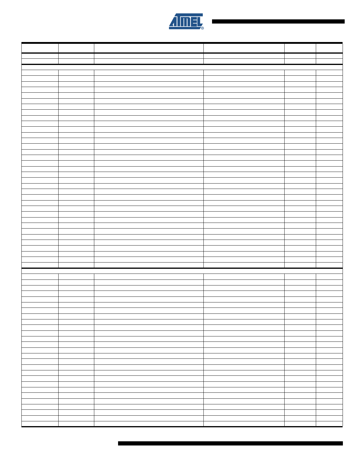
Instruction Set Summary
Mnemonics
Operands
Description
Operation
Flags
#Clocks
ARITHMETIC AND LOGIC INSTRUCTIONS
ADD
Rd, Rr
Add two Registers
Rd
← Rd + Rr
Z,C,N,V,H
1
ADC
Rd, Rr
Add with Carry two Registers
Rd
← Rd + Rr + C
Z,C,N,V,H
1
ADIW
Rdl,K
Add Immediate to Word
Rdh:Rdl
← Rdh:Rdl + K
Z,C,N,V,S
2
SUB
Rd, Rr
Subtract two Registers
Rd
← Rd - Rr
Z,C,N,V,H
1
SUBI
Rd, K
Subtract Constant from Register
Rd
← Rd - K
Z,C,N,V,H
1
SBC
Rd, Rr
Subtract with Carry two Registers
Rd
← Rd - Rr - C
Z,C,N,V,H
1
SBCI
Rd, K
Subtract with Carry Constant from Reg.
Rd
← Rd - K - C
Z,C,N,V,H
1
SBIW
Rdl,K
Subtract Immediate from Word
Rdh:Rdl
← Rdh:Rdl - K
Z,C,N,V,S
2
AND
Rd, Rr
Logical AND Registers
Rd
← Rd • Rr
Z,N,V
1
ANDI
Rd, K
Logical AND Register and Constant
Rd
← Rd • K
Z,N,V
1
OR
Rd, Rr
Logical OR Registers
Rd
← Rd v Rr
Z,N,V
1
ORI
Rd, K
Logical OR Register and Constant
Rd
← Rd v K
Z,N,V
1
EOR
Rd, Rr
Exclusive OR Registers
Rd
← Rd ⊕ Rr
Z,N,V
1
COM
Rd
One’s Complement
Rd
← $FF − Rd
Z,C,N,V
1
NEG
Rd
Two’s Complement
Rd
← $00 − Rd
Z,C,N,V,H
1
SBR
Rd,K
Set Bit(s) in Register
Rd
← Rd v K
Z,N,V
1
CBR
Rd,K
Clear Bit(s) in Register
Rd
← Rd • ($FF - K)
Z,N,V
1
INC
Rd
Increment
Rd
← Rd + 1
Z,N,V
1
DEC
Rd
Decrement
Rd
← Rd − 1
Z,N,V
1
TST
Rd
Test for Zero or Minus
Rd
← Rd • Rd
Z,N,V
1
CLR
Rd
Clear Register
Rd
← Rd ⊕ Rd
Z,N,V
1
SER
Rd
Set Register
Rd
← $FF
None
1
MUL
Rd, Rr
Multiply Unsigned
R1:R0
← Rd x Rr
Z,C
2
MULS
Rd, Rr
Multiply Signed
R1:R0
← Rd x Rr
Z,C
2
MULSU
Rd, Rr
Multiply Signed with Unsigned
R1:R0
← Rd x Rr
Z,C
2
FMUL
Rd, Rr
Fractional Multiply Unsigned
R1:R0
← (Rd x Rr)
<< 1
Z,C
2
FMULS
Rd, Rr
Fractional Multiply Signed
R1:R0
← (Rd x Rr)
<< 1
Z,C
2
FMULSU
Rd, Rr
Fractional Multiply Signed with Unsigned
R1:R0
← (Rd x Rr)
<< 1
Z,C
2
BRANCH INSTRUCTIONS
RJMP
k
Relative Jump
PC
← PC + k + 1
None
2
IJMP
Indirect Jump to (Z)
PC
← Z
None
2
JMP
k
Direct Jump
PC
← k
None
3
RCALL
k
Relative Subroutine Call
PC
← PC + k + 1
None
3
ICALL
Indirect Call to (Z)
PC
← Z
None
3
CALL
k
Direct Subroutine Call
PC
← k
None
4
RET
Subroutine Return
PC
← STACK
None
4
RETI
Interrupt Return
PC
← STACK
I
4
CPSE
Rd,Rr
Compare, Skip if Equal
if (Rd = Rr) PC
← PC + 2 or 3
None
1 / 2 / 3
CP
Rd,Rr
Compare
Rd
− Rr
Z, N,V,C,H
1
CPC
Rd,Rr
Compare with Carry
Rd
− Rr − C
Z, N,V,C,H
1
CPI
Rd,K
Compare Register with Immediate
Rd
− K
Z, N,V,C,H
1
SBRC
Rr, b
Skip if Bit in Register Cleared
if (Rr(b)=0) PC
← PC + 2 or 3
None
1 / 2 / 3
SBRS
Rr, b
Skip if Bit in Register is Set
if (Rr(b)=1) PC
← PC + 2 or 3
None
1 / 2 / 3
SBIC
P, b
Skip if Bit in I/O Register Cleared
if (P(b)=0) PC
← PC + 2 or 3
None
1 / 2 / 3
SBIS
P, b
Skip if Bit in I/O Register is Set
if (P(b)=1) PC
← PC + 2 or 3
None
1 / 2 / 3
BRBS
s, k
Branch if Status Flag Set
if (SREG(s) = 1) then PC
←PC+k + 1
None
1 / 2
BRBC
s, k
Branch if Status Flag Cleared
if (SREG(s) = 0) then PC
←PC+k + 1
None
1 / 2
BREQ
k
Branch if Equal
if (Z = 1) then PC
← PC + k + 1
None
1 / 2
BRNE
k
Branch if Not Equal
if (Z = 0) then PC
← PC + k + 1
None
1 / 2
BRCS
k
Branch if Carry Set
if (C = 1) then PC
← PC + k + 1
None
1 / 2
BRCC
k
Branch if Carry Cleared
if (C = 0) then PC
← PC + k + 1
None
1 / 2
BRSH
k
Branch if Same or Higher
if (C = 0) then PC
← PC + k + 1
None
1 / 2
BRLO
k
Branch if Lower
if (C = 1) then PC
← PC + k + 1
None
1 / 2
BRMI
k
Branch if Minus
if (N = 1) then PC
← PC + k + 1
None
1 / 2
BRPL
k
Branch if Plus
if (N = 0) then PC
← PC + k + 1
None
1 / 2
BRGE
k
Branch if Greater or Equal, Signed
if (N
⊕ V= 0) then PC ← PC + k + 1
None
1 / 2
BRLT
k
Branch if Less Than Zero, Signed
if (N
⊕ V= 1) then PC ← PC + k + 1
None
1 / 2
BRHS
k
Branch if Half Carry Flag Set
if (H = 1) then PC
← PC + k + 1
None
1 / 2
BRHC
k
Branch if Half Carry Flag Cleared
if (H = 0) then PC
← PC + k + 1
None
1 / 2
BRTS
k
Branch if T Flag Set
if (T = 1) then PC
← PC + k + 1
None
1 / 2
BRTC
k
Branch if T Flag Cleared
if (T = 0) then PC
← PC + k + 1
None
1 / 2
BRVS
k
Branch if Overflow Flag is Set
if (V = 1) then PC
← PC + k + 1
None
1 / 2
BRVC
k
Branch if Overflow Flag is Cleared
if (V = 0) then PC
← PC + k + 1
None
1 / 2
10
2466TS–AVR–07/10
ATmega16(L)
BRIE
k
Branch if Interrupt Enabled
if ( I = 1) then PC
← PC + k + 1
None
1 / 2
BRID
k
Branch if Interrupt Disabled
if ( I = 0) then PC
← PC + k + 1
None
1 / 2
DATA TRANSFER INSTRUCTIONS
MOV
Rd, Rr
Move Between Registers
Rd
← Rr
None
1
MOVW
Rd, Rr
Copy Register Word
Rd+1:Rd
← Rr+1:Rr
None
1
LDI
Rd, K
Load Immediate
Rd
← K
None
1
LD
Rd, X
Load Indirect
Rd
← (X)
None
2
LD
Rd, X+
Load Indirect and Post-Inc.
Rd
← (X), X ← X + 1
None
2
LD
Rd, - X
Load Indirect and Pre-Dec.
X
← X - 1, Rd ← (X)
None
2
LD
Rd, Y
Load Indirect
Rd
← (Y)
None
2
LD
Rd, Y+
Load Indirect and Post-Inc.
Rd
← (Y), Y ← Y + 1
None
2
LD
Rd, - Y
Load Indirect and Pre-Dec.
Y
← Y - 1, Rd ← (Y)
None
2
LDD
Rd,Y+q
Load Indirect with Displacement
Rd
← (Y + q)
None
2
LD
Rd, Z
Load Indirect
Rd
← (Z)
None
2
LD
Rd, Z+
Load Indirect and Post-Inc.
Rd
← (Z), Z ← Z+1
None
2
LD
Rd, -Z
Load Indirect and Pre-Dec.
Z
← Z - 1, Rd ← (Z)
None
2
LDD
Rd, Z+q
Load Indirect with Displacement
Rd
← (Z + q)
None
2
LDS
Rd, k
Load Direct from SRAM
Rd
← (k)
None
2
ST
X, Rr
Store Indirect
(X)
← Rr
None
2
ST
X+, Rr
Store Indirect and Post-Inc.
(X)
← Rr, X ← X + 1
None
2
ST
- X, Rr
Store Indirect and Pre-Dec.
X
← X - 1, (X) ← Rr
None
2
ST
Y, Rr
Store Indirect
(Y)
← Rr
None
2
ST
Y+, Rr
Store Indirect and Post-Inc.
(Y)
← Rr, Y ← Y + 1
None
2
ST
- Y, Rr
Store Indirect and Pre-Dec.
Y
← Y - 1, (Y) ← Rr
None
2
STD
Y+q,Rr
Store Indirect with Displacement
(Y + q)
← Rr
None
2
ST
Z, Rr
Store Indirect
(Z)
← Rr
None
2
ST
Z+, Rr
Store Indirect and Post-Inc.
(Z)
← Rr, Z ← Z + 1
None
2
ST
-Z, Rr
Store Indirect and Pre-Dec.
Z
← Z - 1, (Z) ← Rr
None
2
STD
Z+q,Rr
Store Indirect with Displacement
(Z + q)
← Rr
None
2
STS
k, Rr
Store Direct to SRAM
(k)
← Rr
None
2
LPM
Load Program Memory
R0
← (Z)
None
3
LPM
Rd, Z
Load Program Memory
Rd
← (Z)
None
3
LPM
Rd, Z+
Load Program Memory and Post-Inc
Rd
← (Z), Z ← Z+1
None
3
SPM
Store Program Memory
(Z)
← R1:R0
None
-
IN
Rd, P
In Port
Rd
← P
None
1
OUT
P, Rr
Out Port
P
← Rr
None
1
PUSH
Rr
Push Register on Stack
STACK
← Rr
None
2
POP
Rd
Pop Register from Stack
Rd
← STACK
None
2
BIT AND BIT-TEST INSTRUCTIONS
SBI
P,b
Set Bit in I/O Register
I/O(P,b)
← 1
None
2
CBI
P,b
Clear Bit in I/O Register
I/O(P,b)
← 0
None
2
LSL
Rd
Logical Shift Left
Rd(n+1)
← Rd(n), Rd(0) ← 0
Z,C,N,V
1
LSR
Rd
Logical Shift Right
Rd(n)
← Rd(n+1), Rd(7) ← 0
Z,C,N,V
1
ROL
Rd
Rotate Left Through Carry
Rd(0)
←C,Rd(n+1)← Rd(n),C←Rd(7)
Z,C,N,V
1
ROR
Rd
Rotate Right Through Carry
Rd(7)
←C,Rd(n)← Rd(n+1),C←Rd(0)
Z,C,N,V
1
ASR
Rd
Arithmetic Shift Right
Rd(n)
← Rd(n+1), n=0..6
Z,C,N,V
1
SWAP
Rd
Swap Nibbles
Rd(3..0)
←Rd(7..4),Rd(7..4)←Rd(3..0)
None
1
BSET
s
Flag Set
SREG(s)
← 1
SREG(s)
1
BCLR
s
Flag Clear
SREG(s)
← 0
SREG(s)
1
BST
Rr, b
Bit Store from Register to T
T
← Rr(b)
T
1
BLD
Rd, b
Bit load from T to Register
Rd(b)
← T
None
1
SEC
Set Carry
C
← 1
C
1
CLC
Clear Carry
C
← 0
C
1
SEN
Set Negative Flag
N
← 1
N
1
CLN
Clear Negative Flag
N
← 0
N
1
SEZ
Set Zero Flag
Z
← 1
Z
1
CLZ
Clear Zero Flag
Z
← 0
Z
1
SEI
Global Interrupt Enable
I
← 1
I
1
CLI
Global Interrupt Disable
I
← 0
I
1
SES
Set Signed Test Flag
S
← 1
S
1
CLS
Clear Signed Test Flag
S
← 0
S
1
SEV
Set Twos Complement Overflow.
V
← 1
V
1
CLV
Clear Twos Complement Overflow
V
← 0
V
1
SET
Set T in SREG
T
← 1
T
1
CLT
Clear T in SREG
T
← 0
T
1
SEH
Set Half Carry Flag in SREG
H
← 1
H
1
Mnemonics
Operands
Description
Operation
Flags
#Clocks