
©
2005 Microchip Technology Inc.
DS21435F-page 1
TC55
Features
• Low Dropout Voltage: 120 mV (typ) at 100 mA,
380 mV (typ) at 200 mA
• High Output Current: 250 mA (V
OUT
= 5.0V)
• High Accuracy Output Voltage: ±2% (max)
(±1% Semi-Custom Version)
• Low Power Consumption: 1.1 µA (typ)
• Low Temperature Drift: ±100 ppm/°C (typ)
• Excellent Line Regulation: 0.2%/V (typ)
• Package Options: 3-Pin SOT-23A, 3-Pin SOT-89
and 3-Pin TO-92
• Short-Circuit Protection
• Standard Output Voltage Options: 1.2V, 1.8V,
2.5V, 3.0V, 3.3V, 5.0V
Applications
• Battery-Powered Devices
• Cameras and Portable Video Equipment
• Pagers and Cellular Phones
• Solar Powered Instruments
• Consumer Products
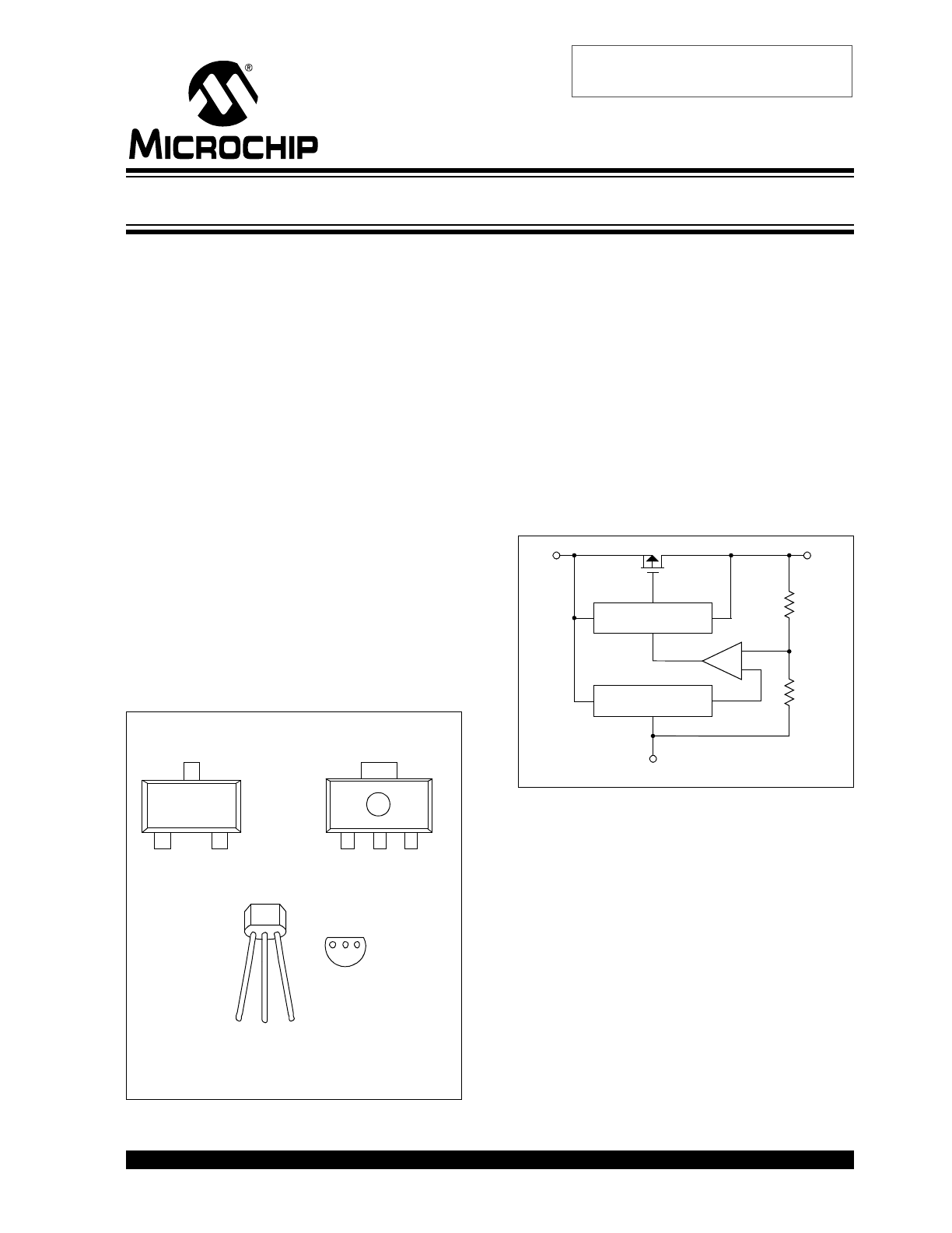
Package Types
General Description
The TC55 Series is a collection of CMOS low dropout,
positive voltage regulators that can source up to
250 mA of current, with an extremely low input-output
voltage differential of 380 mV (typ) at 200 mA.
The TC55’s low dropout voltage, combined with the low
current consumption of only 1.1 µA (typ), makes it ideal
for battery operation. The low voltage differential (drop-
out voltage) extends the battery operating lifetime. It
also permits high currents in small packages when
operated with minimum V
IN
– V
OUT
differentials.
The circuit also incorporates short-circuit protection to
ensure maximum reliability.
Functional Block Diagram
V
IN
GND
V
OUT
3
1
2
TC55
GND V
IN
V
OUT
1
2
3
TC55
3-Pin SOT-23A
3-Pin SOT-89
3-Pin TO-92
1 2 3
V
OUT
V
IN
GND
Note: 3-Pin SOT-23A is equivalent to the
EIAJ SC-59.
V
IN
Bottom
View
V
IN
V
OUT
GND
Short-Circuit
Protection
Voltage
Reference
+
–
1 µA Low Dropout Positive Voltage Regulator
Obsolete Device
TC55
DS21435F-page 2
©
2005 Microchip Technology Inc.
1.0
ELECTRICAL
CHARACTERISTICS
Absolute Maximum Ratings†
Input Voltage ........................................................+12V
Output Current (Continuous) ......... P
D
/(V
IN
– V
OUT
)mA
Output Current (peak) ..................................... 500 mA
Output Voltage.................. (V
SS
– 0.3V) to (V
IN
+ 0.3V)
Continuous Power Dissipation:
3-Pin SOT-23A ..........................................240 mW
3-Pin SOT-89 ............................................500 mW
3-Pin TO-92...............................................440 mW
† Stresses above those listed under "Absolute Maximum
Ratings" may cause permanent damage to the device. These
are stress ratings only and functional operation of the device
at these or any other conditions above those indicated in the
operation sections of the specifications is not implied.
Exposure to Absolute Maximum Rating conditions for
extended periods may affect device reliability.
PIN FUNCTION TABLE
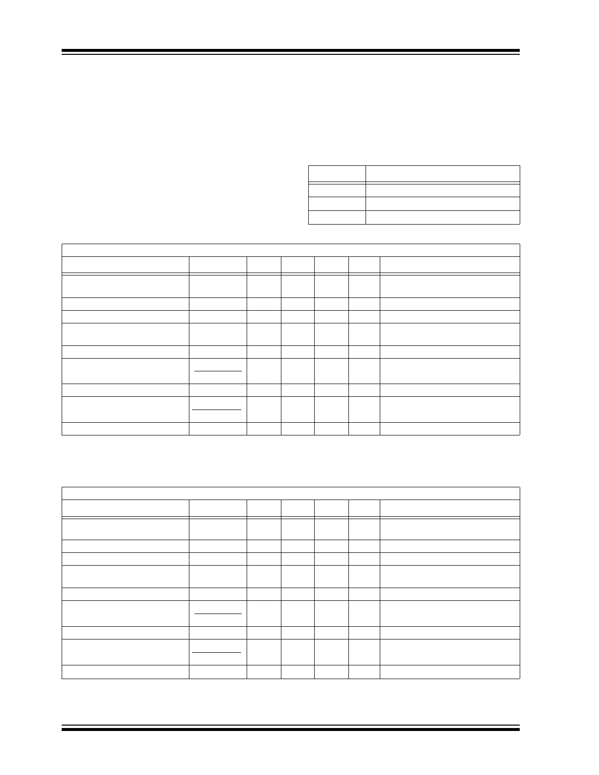
TC55RP50: ELECTRICAL CHARACTERISTICS
TC55RP40: ELECTRICAL CHARACTERISTICS
Symbol
Description
GND
Ground Terminal
V
OUT
Regulated Voltage Output
V
IN
Unregulated Supply Input
Electrical Specifications: Unless otherwise specified, V
OUT
(S) = 5.0V, T
A
= +25°C (see Note 1).
Parameters
Sym
Min
Typ
Max
Units
Conditions
Output Voltage
V
OUT
(A)
—
4.90
—
5.0
—
5.10
V
I
OUT
= 40 mA
V
IN
= 6.0V
Maximum Output Current
I
OUT
MAX
250
—
—
mA
V
IN
= 6.0V, V
OUT
(A)
≥
4.5V
Load Regulation
Δ
V
OUT
—
40
80
mV
V
IN
= 6.0V, 1 mA
≤
I
OUT
≤
100 mA
I/O Voltage Difference
V
DIF
—
—
120
380
300
600
mV
I
OUT
= 100 mA
I
OUT
= 200 mA
Current Consumption
I
SS
—
1.1
3.0
µA
V
IN
= 6.0V
Voltage Regulation
V
OUT
(A)•100
Δ
V
IN
•V
OUT
(S)
—
0.2
0.3
%/V
I
OUT
= 40 mA, 6.0V
≤
V
IN
≤
10.0V
Input Voltage
V
IN
—
—
10
V
Temperature Coefficient of Output
Voltage
Δ
V
OUT
(A)•10
6
V
OUT
(S)•
Δ
T
A
—
±100
—
ppm/°C I
OUT
= 40 mA, -40°C
≤
T
A
≤ +
85°C
Long-Term Stability
—
0.5
—
%
T
A
= +125°C, 1000 Hours
Note
1:
V
OUT
(S): Preset value of output voltage; V
OUT
(A): Actual value of output voltage; V
DIF
: Definition of I/O voltage
difference = {V
IN
1 – V
OUT
(A)}; V
OUT
(A): Output voltage when I
OUT
is fixed and V
IN
= V
OUT
(S) + 1.0V; V
IN
1: Input voltage
when the output voltage is 98% V
OUT
(A).
Electrical Specifications: Unless otherwise specified, V
OUT
(S) = 4.0V, T
A
= +25°C (see Note 1).
Parameters
Sym
Min
Typ
Max
Units
Conditions
Output Voltage
V
OUT
(A)
—
3.92
—
4.0
—
4.08
V
I
OUT
= 40 mA
V
IN
= 5.0V
Maximum Output Current
I
OUT
MAX
200
—
—
mA
V
IN
= 5.0V, V
OUT
(A)
≥
3.6V
Load Regulation
Δ
V
OUT
—
45
90
mV
V
IN
= 5.0V, 1 mA
≤
I
OUT
≤
100 mA
I/O Voltage Difference
V
DIF
—
—
170
400
330
630
mV
I
OUT
= 100 mA
I
OUT
= 200 mA
Current Consumption
I
SS
—
1.0
2.9
µA
V
IN
= 5.0V
Voltage Regulation
V
OUT
(A)•100
Δ
V
IN
•V
OUT
(S)
—
0.2
0.3
%/V
I
OUT
= 40 mA, 5.0V
≤
V
IN
≤
10.0V
Input Voltage
V
IN
—
—
10
V
Temperature Coefficient of Output
Voltage
Δ
V
OUT
(A)•10
6
V
OUT
(S)•
Δ
T
A
—
±100
—
ppm/°C I
OUT
= 40 mA, -40°C
≤
T
A
≤ +
85°C
Long-Term Stability
—
0.5
—
%
T
A
= +125°C, 1000 Hours
Note
1:
V
OUT
(S): Preset value of output voltage; V
OUT
(A): Actual value of output voltage; V
DIF
: Definition of I/O voltage
difference = {V
IN
1 – V
OUT
(A)}; V
OUT
(A): Output voltage when I
OUT
is fixed and V
IN
= V
OUT
(S) + 1.0V; V
IN
1: Input voltage
when the output voltage is 98% V
OUT
(A).
©
2005 Microchip Technology Inc.
DS21435F-page 3
TC55
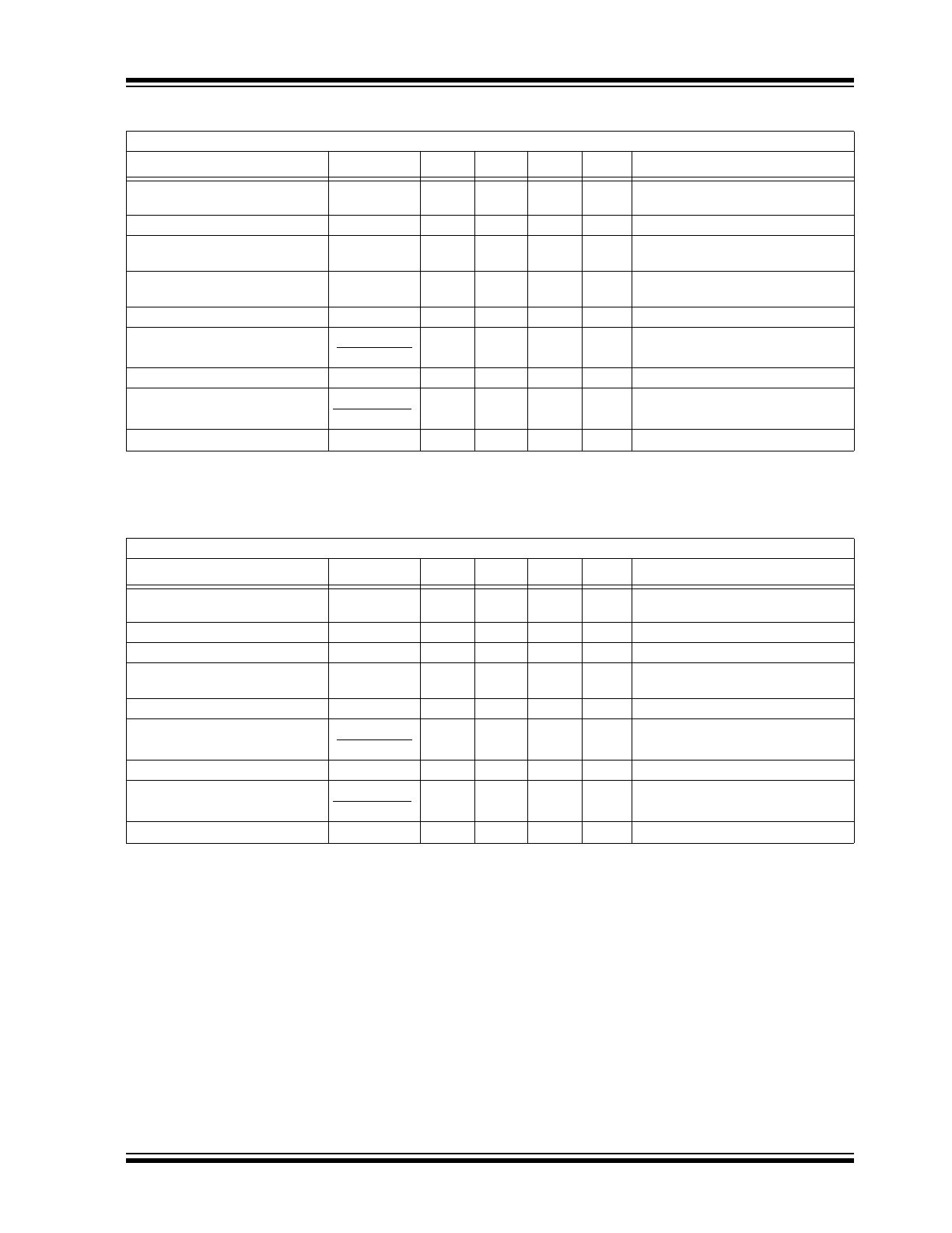
TC55RP33: ELECTRICAL CHARACTERISTICS
TC55RP30: ELECTRICAL CHARACTERISTICS
Electrical Specifications: Unless otherwise specified, V
OUT
(S) = 3.3V, T
A
= +25°C (see Note 1).
Parameters
Sym
Min
Typ
Max
Units
Conditions
Output Voltage
V
OUT
(A)
—
3.23
—
3.30
—
3.37
V
I
OUT
= 40 mA
V
IN
= 4.3V
Maximum Output Current
I
OUT
MAX
150
—
—
mA
V
IN
= 4.3V, V
OUT
(A)
≥
3.0V
Load Regulation
Δ
V
OUT
—
45
90
mV
V
IN
= 4.3V,
1 mA
≤
I
OUT
≤
80 mA
I/O Voltage Difference
V
DIF
—
—
180
400
360
700
mV
I
OUT
= 80 mA
I
OUT
= 160 mA
Current Consumption
I
SS
—
1.0
2.9
µA
V
IN
= 4.3V
Voltage Regulation
V
OUT
(A)•100
Δ
V
IN
•V
OUT
(S)
—
0.2
0.3
%/V
I
OUT
= 40 mA,
4.3V
≤
I
OUT
≤
10.0V
Input Voltage
V
IN
—
—
10
V
Temperature Coefficient of Output
Voltage
Δ
V
OUT
(A)•10
6
V
OUT
(S)•
Δ
T
A
—
±100
—
ppm/°C I
OUT
= 40 mA, -40°C
≤
T
A
≤ +
85°C
Long-Term Stability
—
0.5
—
%
T
A
= +125°C, 1,000 Hours
Note
1:
V
OUT
(S): Preset value of output voltage; V
OUT
(A): Actual value of output voltage; V
DIF
: Definition of I/O voltage
difference = {V
IN
1 – V
OUT
(A)}; V
OUT
(A): Output voltage when I
OUT
is fixed and V
IN
= V
OUT
(S) + 1.0V; V
IN
1: Input voltage
when the output voltage is 98% V
OUT
(A).
Electrical Specifications: Unless otherwise specified, V
OUT
(S) = 3.0V, T
A
= +25°C (see Note 1).
Parameters
Sym
Min
Typ
Max
Units
Conditions
Output Voltage
V
OUT
(A)
—
2.94
—
3.0
—
3.06
V
I
OUT
= 40 mA
V
IN
= 4.0V
Maximum Output Current
I
OUT
MAX
150
—
—
mA
V
IN
= 4.0V, V
OUT
(A)
≥
2.7V
Load Regulation
Δ
V
OUT
—
45
90
mV
V
IN
= 4.0V, 1 mA
≤
I
OUT
≤
80 mA
I/O Voltage Difference
V
DIF
—
—
180
400
360
700
mV
I
OUT
= 80 mA
I
OUT
= 160 mA
Current Consumption
I
SS
—
0.9
2.8
µA
V
IN
= 4.0V
Voltage Regulation
V
OUT
(A)•100
Δ
V
IN
•V
OUT
(S)
—
0.2
0.3
%/V
I
OUT
= 40 mA, 4.0V
≤
V
IN
≤
10.0V
Input Voltage
V
IN
—
—
10
V
Temperature Coefficient of Output
Voltage
Δ
V
OUT
(A)•10
6
V
OUT
(S)•
Δ
T
A
—
±100
—
ppm/°C I
OUT
= 40 mA, -40°C
≤
T
A
≤ +
85°C
Long-Term Stability
—
0.5
—
%
T
A
= +125°C, 1000 Hours
Note
1:
V
OUT
(S): Preset value of output voltage; V
OUT
(A): Actual value of output voltage; V
DIF
: Definition of I/O voltage
difference = {V
IN
1 – V
OUT
(A)}; V
OUT
(A): Output voltage when I
OUT
is fixed and V
IN
= V
OUT
(S) + 1.0V; V
IN
1: Input voltage
when the output voltage is 98% V
OUT
(A).
TC55
DS21435F-page 4
©
2005 Microchip Technology Inc.
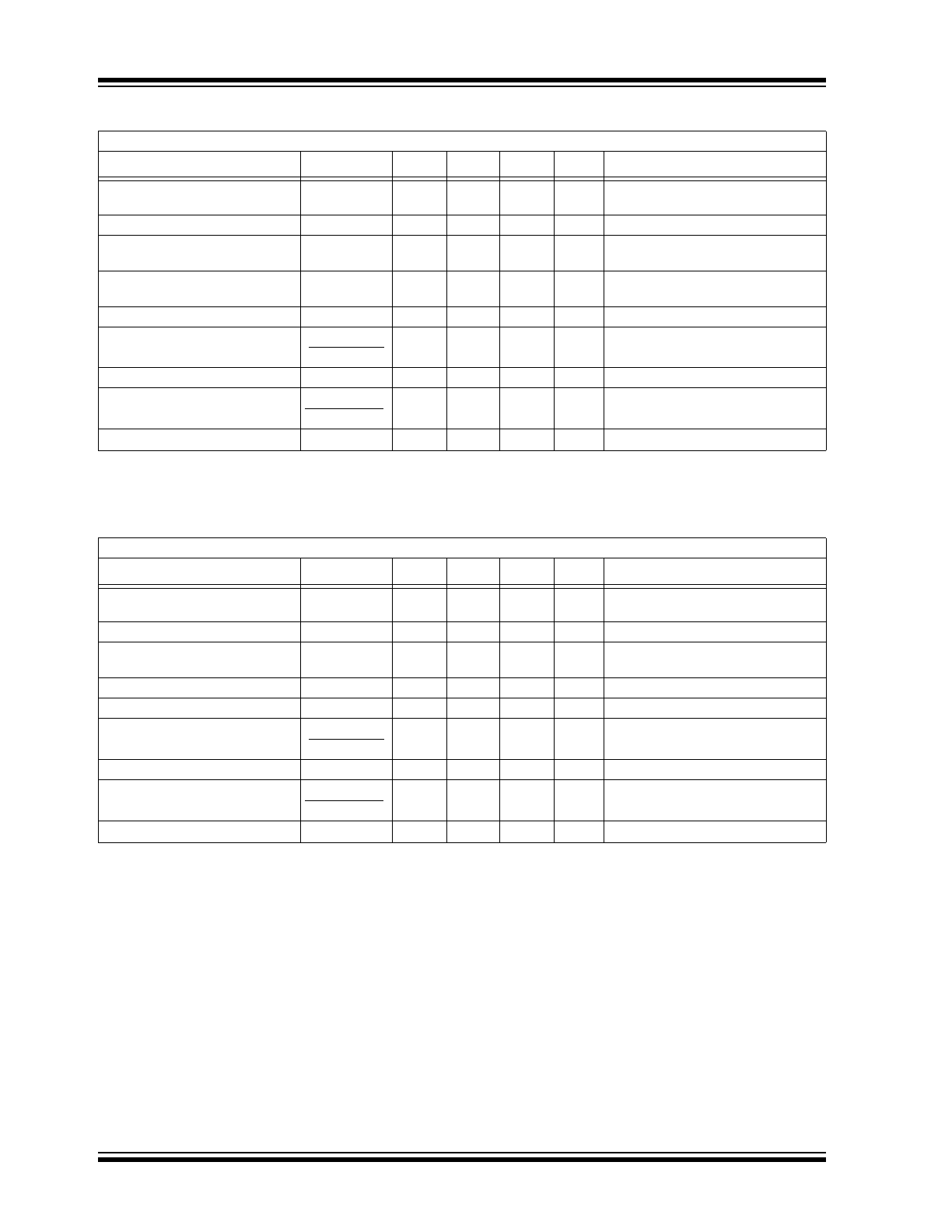
TC55RP25: ELECTRICAL CHARACTERISTICS
TC55RP18: ELECTRICAL CHARACTERISTICS
Electrical Specifications: Unless otherwise specified, V
OUT
(S) = 2.5V, T
A
= +25°C (see Note 1).
Parameters
Sym
Min
Typ
Max
Units
Conditions
Output Voltage
V
OUT
(A)
—
2.45
—
2.5
—
2.55
V
I
OUT
= 40 mA
V
IN
= 3.5V
Maximum Output Current
I
OUT
MAX
125
—
—
mA
V
IN
= 3.5V, V
OUT
(A)
≥
2.25V
Load Regulation
Δ
V
OUT
—
45
90
mV
V
IN
= 3.5V,
1 mA
≤
I
OUT
≤
60 mA
I/O Voltage Difference
V
DIF
—
180
400
360
700
mV
I
OUT
= 60 mA
I
OUT
= 120 mA
Current Consumption
I
SS
—
1.0
2.8
µA
V
IN
= 3.5V
Voltage Regulation
V
OUT
(A)•100
Δ
V
IN
•V
OUT
(S)
—
0.2
0.3
%/V
I
OUT
= 40 mA,
3.5V
≤
I
OUT
≤
10.0V
Input Voltage
V
IN
—
—
10
V
Temperature Coefficient of Output
Voltage
Δ
V
OUT
(A)•10
6
V
OUT
(S)•
Δ
T
A
—
±100
—
ppm/°C I
OUT
= 40 mA, -30°C
≤
T
A
≤ +
80°C
Long-Term Stability
—
0.5
—
%
T
A
= +125°C, 1,000 Hours
Note
1:
V
OUT
(S): Preset value of output voltage; V
OUT
(A): Actual value of output voltage; V
DIF
: Definition of I/O voltage
difference = {V
IN
1 – V
OUT
(A)}; V
OUT
(A): Output voltage when I
OUT
is fixed and V
IN
= V
OUT
(S) + 1.0V; V
IN
1: Input voltage
when the output voltage is 98% V
OUT
(A).
Electrical Specifications: Unless otherwise specified, V
OUT
(S) = 1.8V, T
A
= +25°C (see Note 1).
Parameters
Sym
Min
Typ
Max
Units
Conditions
Output Voltage
V
OUT
(A)
—
1.764
—
1.8
—
1.836
V
I
OUT
= 0.5 mA
V
IN
= 2.8V
Maximum Output Current
I
OUT
MAX
110
—
—
mA
V
IN
= 2.8V, V
OUT
(A)
≥
1.62V
Load Regulation
Δ
V
OUT
—
—
30
mV
V
IN
= 2.8V,
1 mA
≤
I
OUT
≤
30 mA
I/O Voltage Difference
V
DIF
—
—
300
mV
I
OUT
= 0.5 mA
Current Consumption
I
SS
—
—
3.0
µA
V
IN
= 2.8V
Voltage Regulation
V
OUT
(A)•100
Δ
V
IN
•V
OUT
(S)
—
—
0.25
%/V
I
OUT
= 0.5 mA,
2.8V
≤
I
OUT
≤
10.0V
Input Voltage
V
IN
—
—
6.0
V
Temperature Coefficient of Output
Voltage
Δ
V
OUT
(A)•10
6
V
OUT
(S)•
Δ
T
A
—
±100
—
ppm/°C I
OUT
= 0.5 mA, -30°C
≤
T
A
≤ +
80°C
Long-Term Stability
—
0.5
—
%
T
A
= +125°C, 1,000 Hours
Note
1:
V
OUT
(S): Preset value of output voltage; V
OUT
(A): Actual value of output voltage; V
DIF
: Definition of I/O voltage
difference = {V
IN
1 – V
OUT
(A)}; V
OUT
(A): Output voltage when I
OUT
is fixed and V
IN
= V
OUT
(S) + 1.0V; V
IN
1: Input voltage
when the output voltage is 98% V
OUT
(A).
©
2005 Microchip Technology Inc.
DS21435F-page 5
TC55
TC55RP12: ELECTRICAL CHARACTERISTICS
TEMPERATURE CHARACTERISTICS
Electrical Specifications: Unless otherwise specified, V
OUT
(S) = 1.2V, T
A
= +25°C (see Note 1).
Parameters
Sym
Min
Typ
Max
Units
Conditions
Output Voltage
V
OUT
(A)
—
1.176
—
1.200
—
1.224
V
I
OUT
= 0.5 mA
V
IN
= 2.2V
Maximum Output Current
I
OUT
MAX
50
—
—
mA
V
IN
= 2.2V, V
OUT
(A)
≥
1.08V
Load Regulation
Δ
V
OUT
—
—
30
mV
V
IN
= 2.2V,
1 mA
≤
I
OUT
≤
30 mA
I/O Voltage Difference
V
DIF
—
—
300
mV
I
OUT
= 0.5 mA
Current Consumption
I
SS
—
—
3.0
µA
V
IN
= 2.2V
Voltage Regulation
V
OUT
(A)•100
Δ
V
IN
•V
OUT
(S)
—
—
0.25
%/V
I
OUT
= 0.5 ,
2.2V
≤
I
OUT
≤
10.0V
Input Voltage
V
IN
—
—
6.0
V
Temperature Coefficient of Output
Voltage
Δ
V
OUT
(A)•10
6
V
OUT
(S)•
Δ
T
A
—
±100
—
ppm/°C I
OUT
= 0.5 mA, -30°C
≤
T
A
≤ +
80°C
Long-Term Stability
—
0.5
—
%
T
A
= +125°C, 1,000 Hours
Note
1:
V
OUT
(S): Preset value of output voltage; V
OUT
(A): Actual value of output voltage; V
DIF
: Definition of I/O voltage
difference = {V
IN
1 – V
OUT
(A)}; V
OUT
(A): Output voltage when I
OUT
is fixed and V
IN
= V
OUT
(S) + 1.0V; V
IN
1: Input voltage
when the output voltage is 98% V
OUT
(A).
Electrical Specifications: Unless otherwise specified, V
OUT
(S) = 5.0V, T
A
= +25°C.
Parameters
Sym
Min
Typ
Max
Units
Conditions
Temperature Ranges
Specified Temperature Range (E)
T
A
-40
—
+85
ºC
Storage Temperature Range
T
A
-65
—
+150
ºC
Package Thermal Resistances
Thermal Resistance, 3L-SOT-23A
θ
JA
—
359
—
ºC/W
Thermal Resistance, 3L-SOT-89
θ
JA
—
110
—
ºC/W
When mounted on 1 square
inch of copper
Thermal Resistance, 3L-TO-92
θ
JA
—
131.9
—
ºC/W
TC55
DS21435F-page 6
©
2005 Microchip Technology Inc.
2.0
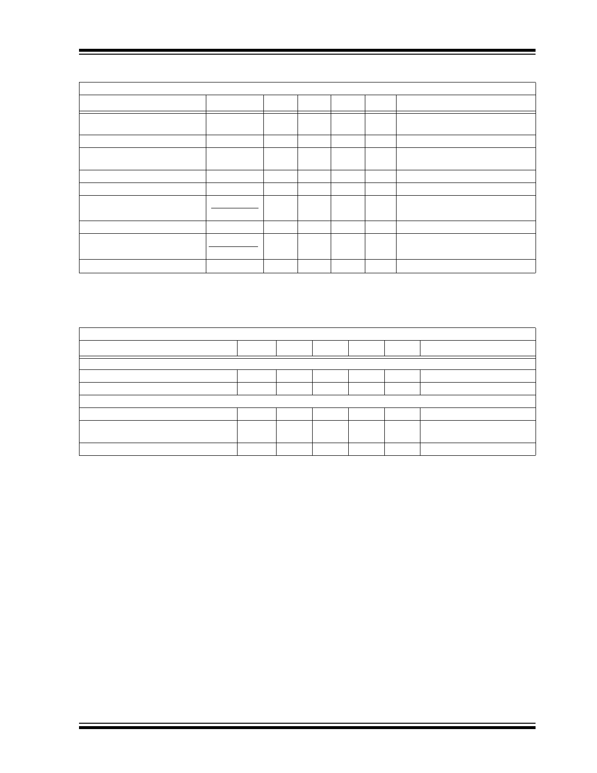
TYPICAL PERFORMANCE CURVES
Notes: Unless otherwise specified, V
OUT
(S) = 3.0V, 5.0V, T
A
= +25°C, C
IN
= 1 µF Tantalum, C
OUT
= 1 µF Tantalum.
FIGURE 2-1:
Output Voltage vs. Output
Current (TC55RP3002).
FIGURE 2-2:
Output Voltage vs. Input
Voltage (TC55RP3002).
FIGURE 2-3:
Output Voltage vs. Input
Voltage (TC55RP3002).
FIGURE 2-4:
Dropout Voltage vs. Output
Current (TC55RP3002).
FIGURE 2-5:
Output Voltage vs.
Operating Temperature (TC55RP3002).
FIGURE 2-6:
Supply Current vs. Input
Voltage (TC55RP3002).
Note:
The graphs and tables provided following this note are a statistical summary based on a limited number of
samples and are provided for informational purposes only. The performance characteristics listed herein
are not tested or guaranteed. In some graphs or tables, the data presented may be outside the specified
operating range (e.g., outside specified power supply range) and therefore outside the warranted range.
2.9
2.8
2.7
20
40
60
0
160
OUTPUT CURRENT I
OUT
(mA)
3.0
3.1
OUTPUT VOLTAGE V
OUT
(V)
80
°C
80 100 120 140
25
°C
-30
°C
V
IN
= 4.0V
T
OPR
= 25
°C
INPUT VOLTAGE V
IN
(V)
2.8
2.6
2.4
2.2
3.0
3.5
2.5
3.0
3.2
OUTPUT VOLTAGE V
OUT
(V)
I
OUT
= 1 mA
10 mA
40 mA
T
OPR
= 25
°C
INPUT VOLTAGE V
IN
(V)
OUTPUT VOLTAGE V
OUT
(V)
3.01
3.00
2.99
2.98
2.96
2.97
2.95
5
6
7
8
9
10
3
4
3.03
3.02
3.05
3.04
I
OUT
= 1 mA
0.8
0.6
0.4
0.2
0.0
-0.2
20 40
60
0
160
OUTPUT CURRENT I
OUT
(mA)
1.4
1.2
1.0
2.0
1.8
1.6
DROPOUT VOLTAGE V
DIF
(V)
80 100 120 140
25
°C
-30
°C
80
°C
OPERATING TEMPERATURE (
°C)
3.02
3.00
2.98
2.96
2.94
2.92
2.90
-40
-20
0
20
40
60
80
100
3.06
3.04
3.10
3.08
OUTPUT VOLTAGE V
OUT
(V)
I
OUT
= 10 mA
40 mA
V
IN
= 4.0V
INPUT VOLTAGE V
IN
(V)
1.1
1.0
0.9
0.8
0.7
0.6
0.5
3
4
5
6
7
8
9
10
1.3
1.2
1.5
1.4
SUPPLY CURRENT I
SS
(
μ
A)
T
OPR
= 25
°
C
©
2005 Microchip Technology Inc.
DS21435F-page 7
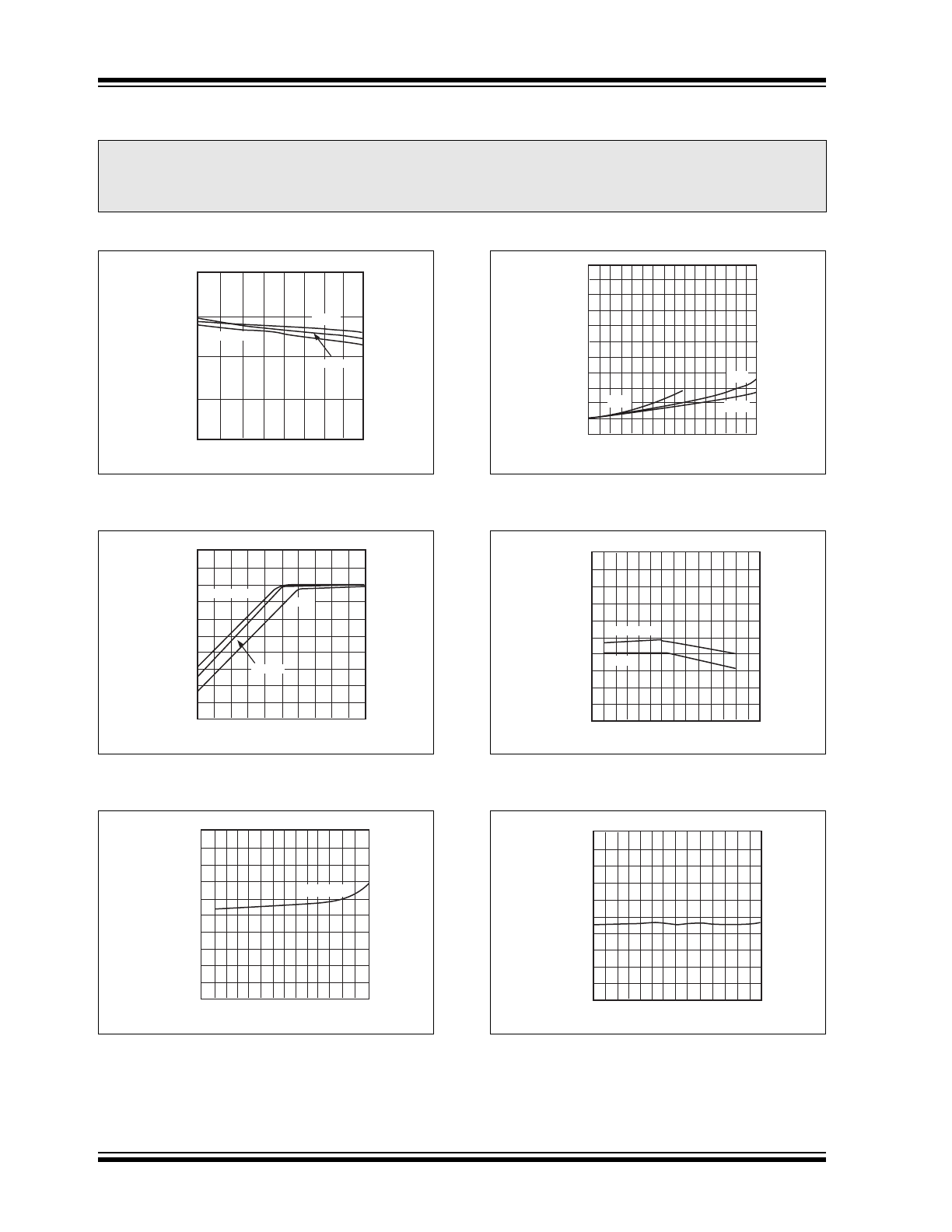
TC55
Note: Unless otherwise indicated, V
OUT
(S) = 3.0V, 5.0V, T
A
= +25°C, C
IN
= 1 µF Tantalum, C
OUT
= 1 µF Tantalum.
FIGURE 2-7:
Supply Current vs.
Operating Temperature (TC55RP3002).
FIGURE 2-8:
Load Transient Response
(TC55RP3002).
FIGURE 2-9:
Output Voltage vs. Output
Current (TC55RP5002).
FIGURE 2-10:
Output Voltage vs. Input
Voltage (TC55RP5002).
FIGURE 2-11:
Output Voltage vs. Input
Voltage (TC55RP5002).
FIGURE 2-12:
Dropout Voltage vs. Output
Current (TC55RP5002).
0.9
0.8
0.7
0.6
0.5
-20
0
20
-40
OPERATING TEMPERATURE (
°C)
1.2
1.1
1.0
1.5
1.4
1.8
40
60
80 100
SUPPLY CURRENT I
SS
(
μ
A)
V
IN
= 4.0V
TIME (2 msec/div)
4
3
2
1
0
40 mA
1 mA
5
200
160
120
80
40
0
OUTPUT VOLTAGE V
OUT
(V)
OUTPUT CURRENT I
OUT
(mA)
Output Current
Output Voltage
OUTPUT CURRENT I
OUT
(mA)
4.9
4.8
4.7
40
80
0
200
160
5.0
5.1
OUTPUT VOLTAGE V
OUT
(V)
120
80
°C
25
°C
-30
°C
V
IN
= 6.0V
INPUT VOLTAGE V
IN
(V)
T
OPR
= 25
°C
4.8
4.6
4.4
4.2
5.0
5.5
4.5
5.0
5.2
OUTPUT VOLTAGE V
OUT
(V)
I
OUT
= 1 mA
10 mA
40 mA
INPUT VOLTAGE V
IN
(V)
T
OPR
= 25
°C
5.01
5.00
4.99
4.97
4.98
4.95
4.98
6
7
8
9
10
5
5.03
5.02
5.04
5.05
OUTPUT VOLTAGE V
OUT
(V)
IOUT = 1 mA
OUTPUT CURRENT I
OUT
(mA)
DROPOUT VOLTAGE V
DIF
(V)
1.0
0.8
0.6
0.4
0.2
0.0
-0.2
40
80
0
200
160
1.4
1.2
2.0
1.8
1.6
120
-30
°C
25
°C
80
°C
TC55
DS21435F-page 8
©
2005 Microchip Technology Inc.
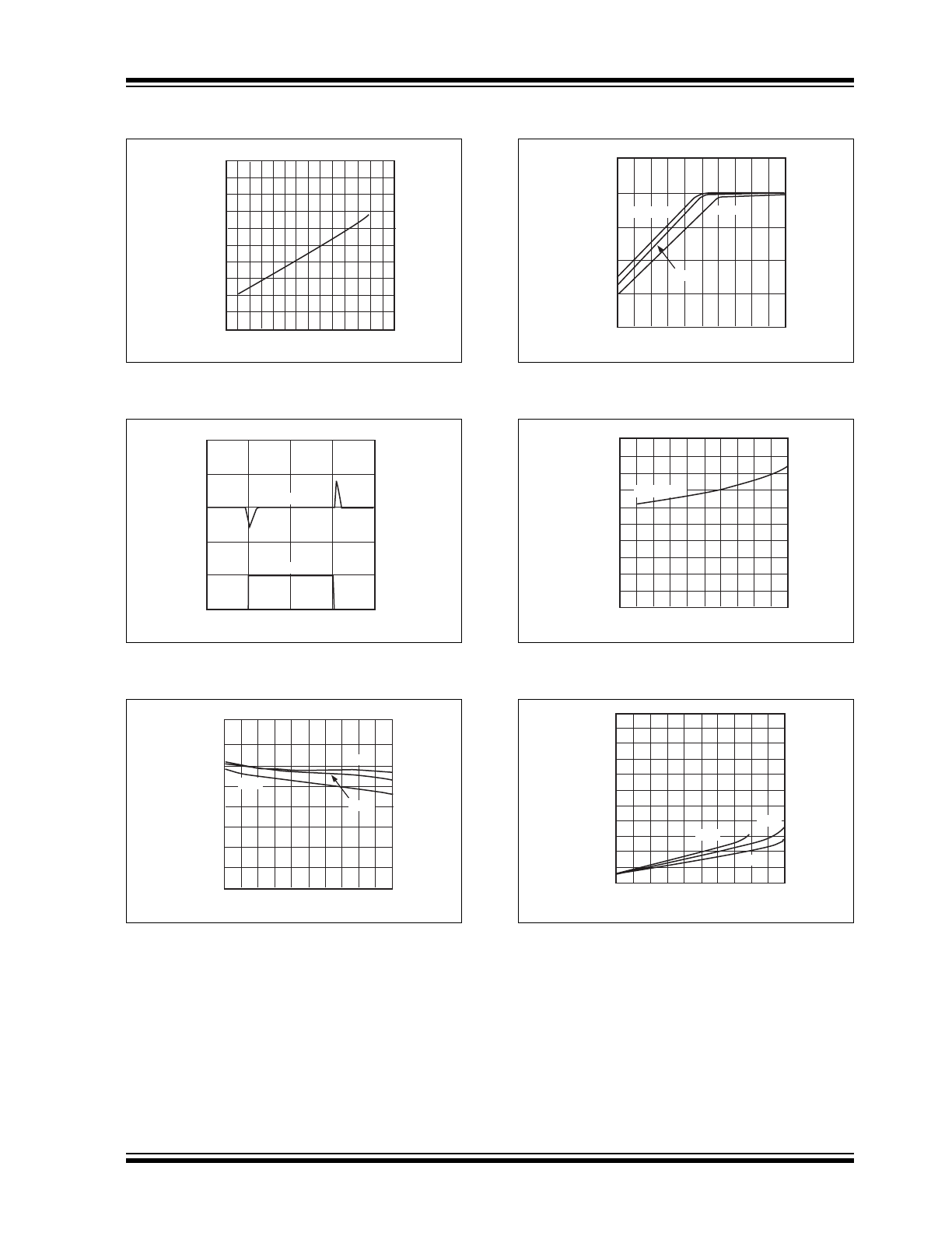
Note: Unless otherwise indicated, V
OUT
(S) = 3.0V, 5.0V, T
A
= +25°C, C
IN
= 1 µF Tantalum, C
OUT
= 1 µF Tantalum.
FIGURE 2-13:
Output Voltage vs.
Operating Temperature (TC55RP5002).
FIGURE 2-14:
Supply Current vs. Input
Voltage (TC55RP5002).
FIGURE 2-15:
Supply Current vs.
Operating Temperature (TC55RP5002).
FIGURE 2-16:
Input Transient Response,
1 mA (TC55RP5002).
FIGURE 2-17:
Input Transient Response,
10 mA (TC55RP5002).
FIGURE 2-18:
Load Transient Response
(TC55RP5002).
OPERATING TEMPERATURE (
°C)
5.02
5.00
4.98
4.96
4.94
4.92
4.90
-40
-20
0
20
40
60
80
100
5.06
5.04
5.10
5.08
OUTPUT VOLTAGE V
OUT
(V)
I
OUT
= 10 mA
40 mA
V
IN
= 6.0V
INPUT VOLTAGE V
IN
(V)
5
6
7
8
9
10
1.6
1.4
1.3
1.2
1.1
1.0
0.5
1.8
1.7
2.0
1.9
SUPPLY CURRENT I
SS
(
μ
A)
T
OPR
= 25
°
C
1.4
1.3
1.2
1.1
1.0
-20
0
20
-40
OPERATING TEMPERATURE (
°C)
1.7
1.6
1.5
2.0
1.9
1.8
40
60
80 100
SUPPLY CURRENT I
SS
(
μ
A)
V
IN
= 6.0V
TIME (msec)
7.0
6.5
6.0
5.5
5.0
5.0
4.5
4.0
-1
0
1
2
3
7.5
Input
Voltage
Output
Voltage
8.0
INPUT VOLTAGE V
OUT
(V)
OUTPUT VOLTAGE V
IN
(V)
I
OUT
= 1 mA
TIME (msec)
7.0
6.5
6.0
5.5
5.0
4.5
4.0
-1
0
1
2
3
7.5
Input
Voltage
Output
Voltage
8.0
INPUT VOLTAGE V
OUT
(V)
OUTPUT VOLTAGE V
OUT
(V)
I
OUT
= 10 mA
TIME (2 msec/div)
6
5
4
3
2
40 mA
1 mA
7
200
160
120
80
40
0
OUTPUT VOLTAGE V
OUT
(V)
OUTPUT CURRENT I
OUT
(mA)
Output Voltage
Output Current
©
2005 Microchip Technology Inc.
DS21435F-page 9
TC55
3.0
PIN DESCRIPTIONS
The descriptions of the pins are listed in Table 3-1.
TABLE 3-1:
PIN FUNCTION TABLE
3.1
Ground Terminal (GND)
Regulator ground. Tie GND to the negative side of the
output and the negative side of the input capacitor.
Only the LDO bias current (1 µA typical) flows out of
this pin, there is no high current. The LDO output regu-
lation is referenced to this pin. Minimize voltage drops
between this pin and the minus side of the load.
3.2
Regulated Voltage Output (V
OUT
)
Connect V
OUT
to the positive side of the load and the
positive terminal of the output capacitor. The positive
side of the output capacitor should be physically
located as close to the LDO V
OUT
pin as is practical.
The current flowing out of this pin is equal to the DC
load current.
3.3
Unregulated Supply Input (V
IN
)
Connect the input supply voltage and the positive side
of the input capacitor to V
IN
. The input capacitor should
be physically located as close as is practical to V
IN
. The
current flow into this pin is equal to the DC load current,
plus the LDO bias current (1 µA typical.)
4.0
DETAILED DESCRIPTION
The TC55 is a low quiescent current, precision, fixed-
output voltage LDO. Unlike bipolar regulators, the
TC55 supply current does not increase proportionally
with load current.
4.1
Output Capacitor
A minimum of 1 µF output capacitor is required. The
output capacitor should have an effective series resis-
tance (esr) greater than 0.1
Ω
and less than 5
Ω
, plus a
resonant frequency above 1 MHz. Larger output
capacitors can be used to improve supply noise rejec-
tion and transient response. Care should be taken
when increasing C
OUT
to ensure that the input imped-
ance is not high enough to cause high input impedance
oscillation.
4.2
Input Capacitor
A 1 µF input capacitor is recommended for most
applications when the input impedance is on the order
of 10
Ω
. Larger input capacitance may be required for
stability when operating off of a battery input, or if there
is a large distance from the input source to the LDO.
When large values of output capacitance are used, the
input capacitance should be increased to prevent high
source impedance oscillations.
Pin No.
Symbol
Description
1
GND
Ground Terminal
2
V
OUT
Regulated Voltage Output
3
V
IN
Unregulated Supply Input
TC55
DS21435F-page 10
©
2005 Microchip Technology Inc.
5.0
THERMAL CONSIDERATIONS
5.1
Power Dissipation
The amount of power dissipated internal to the low
dropout linear regulator is the sum of the power dissi-
pation within the linear pass device (P-Channel MOS-
FET) and the quiescent current required to bias the
internal reference and error amplifier. The internal lin-
ear pass device power dissipation is calculated by mul-
tiplying the voltage across the linear device by the
current through the device.
EQUATION
The internal power dissipation, as a result of the bias
current for the LDO internal reference and error
amplifier, is calculated by multiplying the ground or
quiescent current by the input voltage.
EQUATION
The total internal power dissipation is the sum of P
D
(Pass Device) and P
D
(Bias).
EQUATION
For the TC55, the internal quiescent bias current is so
low (1 µA typical) that the P
D
(Bias) term of the power
dissipation equation can be ignored. The maximum
power dissipation can be estimated by using the
maximum input voltage and the minimum output
voltage to obtain a maximum voltage differential
between input and output. The next step would be to
multiply the maximum voltage differential by the
maximum output current.
EQUATION
Given:
V
IN
= 3.3V to 4.1V
V
OUT
= 3.0 V ± 2%
I
OUT
= 1 mA to 100 mA
T
AMAX
= 55°C
P
MAX
= (4.1V – (3.0V x 0.98)) x 100 mA
P
MAX
= 116.0 milliwatts
To determine the junction temperature of the device, the
thermal resistance from junction-to-ambient must be
known. The 3-pin SOT-23 thermal resistance from junc-
tion-to-air (R
θ
JA
) is estimated to be approximately
359°C/W. The SOT-89 R
θ
JA
is estimated to be approxi-
mately 110°C/W when mounted on 1 square inch of
copper. The TO-92 R
θ
JA
is estimated to be 131.9°C/W.
The R
θ
JA
will vary with physical layout, airflow and other
application-specific conditions.
The device junction temperature is determined by
calculating the junction temperature rise above
ambient, then adding the rise to the ambient
temperature.
EQUATION
P
D
(Pass Device) = (V
IN
– V
OUT
) x I
OUT
P
D
(Bias) = V
IN
x I
GND
P
TOTAL
= P
D
(Pass Device) + P
D
(Bias)
P
D
= (V
INMAX
– V
OUTMIN
) x I
OUTMAX
Junction Temperature
T
J
= P
DMAX
x R
θ
JA
+ T
A
T
J
= 116.0 milliwatts x 359°C/W + 55°C
T
J
= 96.6°C
SOT-23 Example:
SOT-89 Example:
T
J
= 116.0 milliwatts x 110°C/W + 55°C
T
J
= 67.8°C
TO-92 Example:
T
J
= 116.0 milliwatts x 131.9°C/W + 55°C
T
J
= 70.3°C