
2002-2012 Microchip Technology Inc.
DS21429C-page 1
TC51
Features
• Precise Detection Thresholds: ±2.0%
• Small Package: 3-Pin SOT-23A
• Low Supply Current: Typ. 1
A
• Wide Detection Range: 1.6V to 6.0V
• Wide Operating Voltage Range: 0.7V to 10V
• Built-in Delay Circuit: 50msec to 200 msec
• Open-Drain Output
Applications
• Battery Voltage Monitoring
• Microprocessor Reset
• System Brown-out Protection
Device Selection Table
Other output voltages are available. Please contact Microchip
Technology Inc. for details.
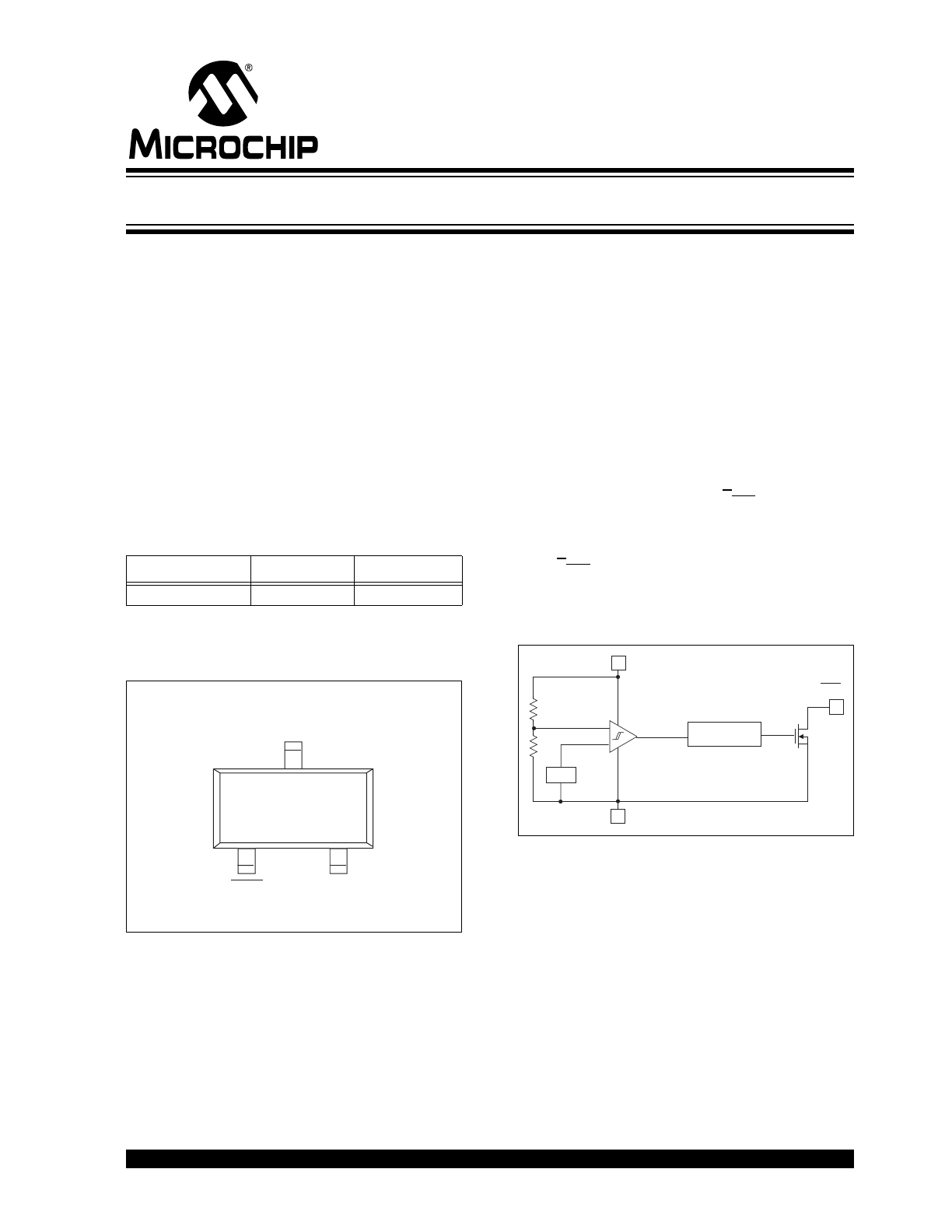
Package Type
General Description
The TC51 is a very low power, open drain output,
CMOS voltage detector with built-in delay. It is
particularly well-suited for battery powered applications
because of its extremely low 1
A operating current and
small surface-mount packaging. Each part is laser-
trimmed to the desired threshold voltage, which can be
specified from 1.6V to 6.0V. The standard built-in
output delay is 50msec-200msec.
The device includes a comparator, low-current high-
precision reference, laser-programmed voltage divider,
hysteresis circuit and output driver with digital delay
timer.
In operation, the TC51’s output (V
OUT
) remains in the
logic HIGH state as long as V
IN
is greater than the
specified threshold voltage (V
DET
-). When V
IN
falls
below V
DET
-, the output is immediately driven to a logic
LOW. V
OUT
remains LOW until V
IN
rises above V
DET
-
by an amount V
HYST
, whereupon it returns to a logic
HIGH after expiration of the built-in delay time.
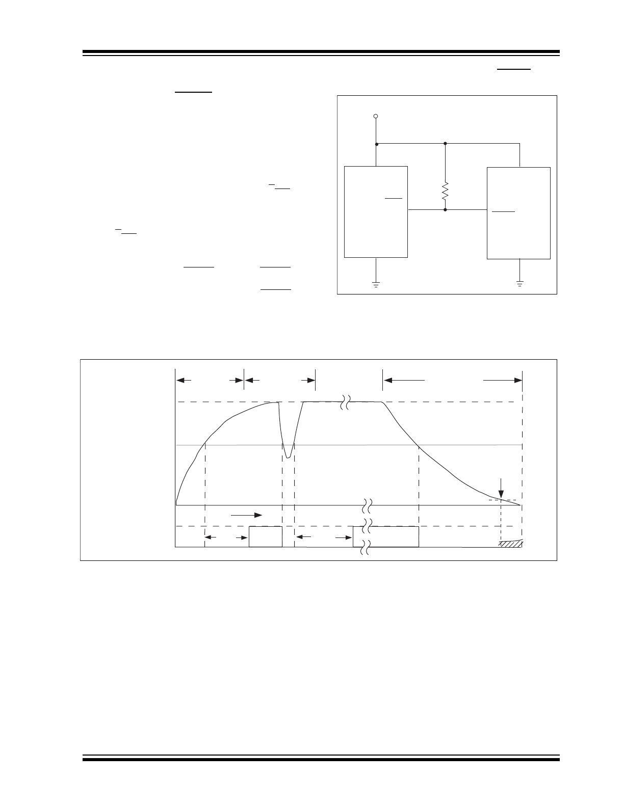
Functional Block Diagram
Part Number
Package
Temp. Range
TC51-xxxxxxxxxx
3-Pin SOT-23A -40°C to +85°C
V
IN
V
OUT
V
SS
TC51
1
2
3
3-Pin SOT-23A
NOTE: 3-Pin SOT-23A is equivalent to the EIAJ SC-59.
V
IN
V
SS
V
OUT
V
REF
Delay
Circuit
1
A Voltage Detector with Output Delay
TC51
DS21429C-page 2
2002-2012 Microchip Technology Inc.
1.0
ELECTRICAL
CHARACTERISTICS
Absolute Maximum Ratings*
Input Voltage ........................................................+12V
Output Current ....................................................50mA
Output Voltage: Open Drain ..........(V
SS
– 0.3V) to 12V
Power Dissipation (T
A
70°C):
3-Pin SOT-23A ...........................................240mW
Operating Temperature Range............. -40°C to +85°C
Storage Temperature Range ..............-65°C to +150°C
*Stresses above those listed under "Absolute Maximum
Ratings" may cause permanent damage to the device. These
are stress ratings only and functional operation of the device
at these or any other conditions above those indicated in the
operation sections of the specifications is not implied.
Exposure to Absolute Maximum Rating conditions for
extended periods may affect device reliability.
TC51 ELECTRICAL SPECIFICATIONS
Electrical Characteristics: T
A
= 25°C, unless otherwise specified.
Symbol
Parameter
Min
Typ
Max
Units
Test Conditions
V
IN
Operating Voltage
0.7
—
10.0
V
(V
DET
-) = 1.6 to 6.0V
I
SS
Quiescent Current
—
—
—
—
—
0.9
1.0
1.3
1.6
2.0
2.6
3.0
3.4
3.8
4.2
A
V
IN
= 1.5V
V
IN
= 2.0V
V
IN
= 3.0V
V
IN
= 4.0V
V
IN
= 5.0V
V
DET
-
Threshold Voltage
V
T
x 0.98
V
T
± 0.5%
V
T
x 1.02
V
Note 1
V
HYST
Hysteresis Voltage
V
DET
- x 0.02
V
DET
- x 0.05
V
DET
- x 0.08
V
I
OUT
Output Current
—
—
2.2
7.7
10.1
11.5
13.0
—
—
mA
V
OL
= 0.5V, V
IN
= 1.0V
V
IN
= 2.0V
V
IN
= 3.0V
V
IN
= 4.0V
V
IN
= 5.0V
T
DLY
Delay Time
50
—
200
msec
Standard
T
C
(V
DET
-)
Tempco of (V
DET
-)
—
±100
—
ppm/°C
-40°C
T
A
85°C
Note
1:
V
T
is the factory programmed threshold voltage setting.
2002-2012 Microchip Technology Inc.
DS21429C-page 3
TC51
2.0
PIN DESCRIPTIONS
The descriptions of the pins are listed in Table 2-1.
TABLE 2-1:
PIN FUNCTION TABLE
Pin No.
(3-Pin SOT-23A)
Symbol
Description
1
V
OUT
Digital output. This output goes low when V
IN
drops below V
DET
- and returns high when V
IN
rises above V
DET
- + V
HYST
. (See Figure 3-1, Timing Diagram).
2
V
SS
Ground terminal.
3
V
IN
Analog input. This pin is both the power supply input and the voltage to be monitored.
TC51
DS21429C-page 4
2002-2012 Microchip Technology Inc.
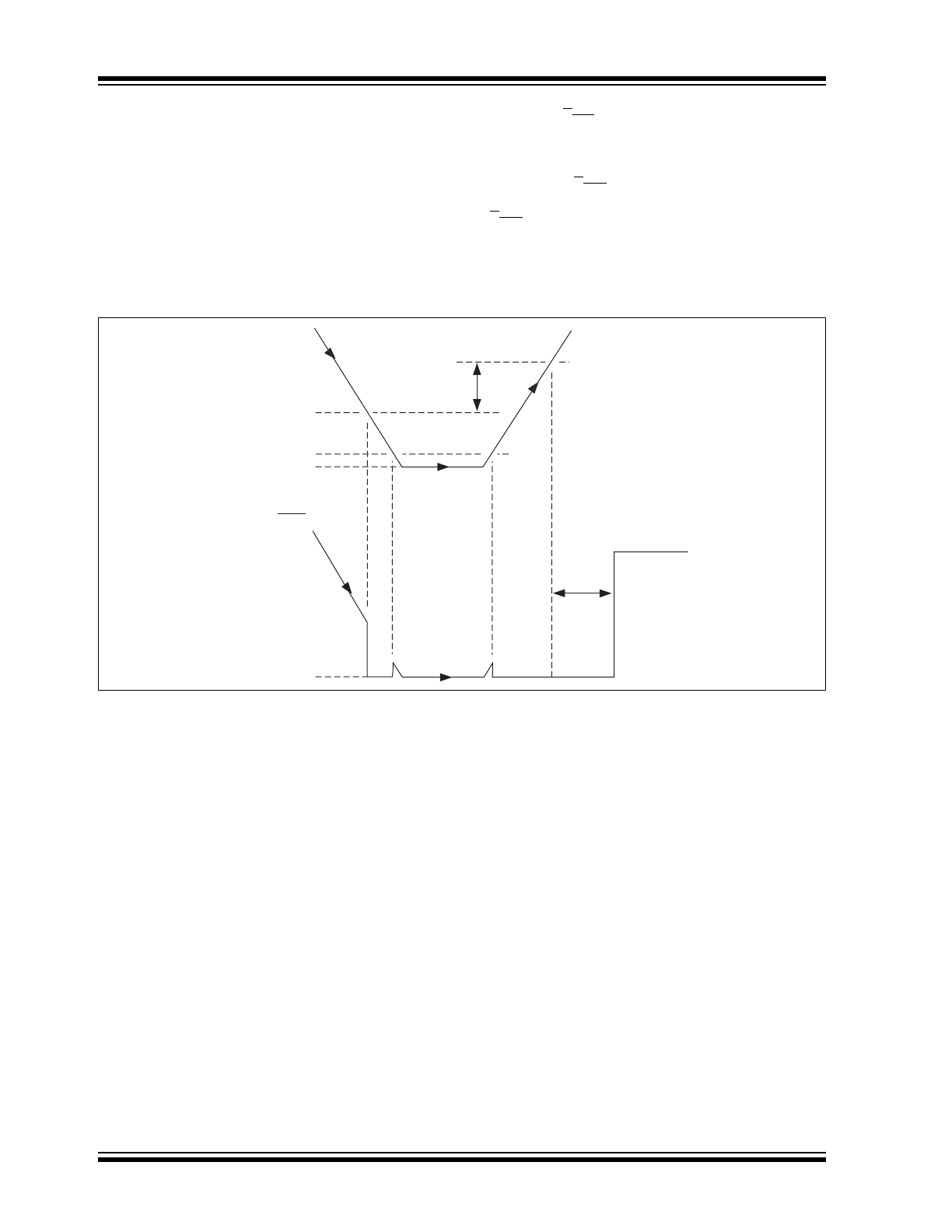
3.0
DETAILED DESCRIPTION
In normal steady-state operation, when V
IN
> V
DET
-,
the output is high, see Figure 3-1. If and when the
input falls below V
DET
-, the output pulls down (Logic 0)
to V
SS
. Generally, V
OUT
can pull down to within 0.5V of
V
SS
at rated output current and input voltage. (Also see
Section 1.0, Electrical Characteristics).
The output, V
OUT
, stays valid until the input voltage falls
below the minimum operating voltage, V
IN
MIN
, of 0.7V.
Below this minimum operating voltage, the output is
undefined. During power-up or anytime V
IN
has fallen
below V
IN
MIN
, V
OUT
will remain undefined until V
IN
rises
above V
IN
MIN
, at which time the output becomes valid.
V
OUT
is maintained in its active low state while
V
IN
MIN
< V
IN
< V
DET
+. (V
DET
+
= V
DET
- + V
HYST
). If and
when the input rises above V
DET
+, the output will
assume its inactive state after Delay Time (T
DLY
).
FIGURE 3-1:
TIMING DIAGRAM
V
IN
Detect Voltage V
DET
-
Minimum Operating
Voltage
V
HYST
V
DET
+
Output Voltage
Release
Voltage
Ground Level
Ground Level
Delay Time (T
DLY
)
V
OUT
2002-2012 Microchip Technology Inc.
DS21429C-page 5
TC51
4.0
APPLICATIONS INFORMATION
4.1
Processor RESET Supervisor
Figure 4-1 shows the TC51 used as a processor reset
supervisor. Because the TC51 is available in threshold
settings of 1.6V to 6.0V, the user can choose the reset
single threshold setting best suited to the system power
supply voltage at hand. Also, the 1
A supply current is
significantly lower than its nearest competitor.
As shown in the timing diagram (Figure 3-1),V
OUT
is
low for voltages between 0.7V and V
DET
+. The TC51
activates its on-board delay timer once the power
supply voltage is within tolerance (i.e., greater than
V
DET
+). V
OUT
is released after delay time (T
DLY
).
Should the power supply voltage momentarily dip
(“brown-out” condition), the TC51 immediately drives
and holds the processor RESET input low. RESET is
released after the power supply voltage is again within
tolerance, and after the delay timer expires. RESET is
driven and held low when power fails (power-off or
“blackout”), and is maintained down low to a supply
voltage of 0.7V.
FIGURE 4-1:
PROCESSOR RESET
SUPERVISOR
FIGURE 4-2:
TC51 OPERATION DURING POWER-UP, BROWN-OUT AND POWER DOWN
TC51
V
OUT
GND
V
DD
V
DD
Processor
RESET
R1
47K
0.7V
Power-Up
Steady
State
Operation
T
DLY
Time
T
DLY
Brown-Out
Power Down
Nominal
Power Supply
Voltage
Threshold
Voltage
(V
DET
-, V
DET
+)
V
OH
TC51 Output
V
OL
TC51
DS21429C-page 6
2002-2012 Microchip Technology Inc.
5.0
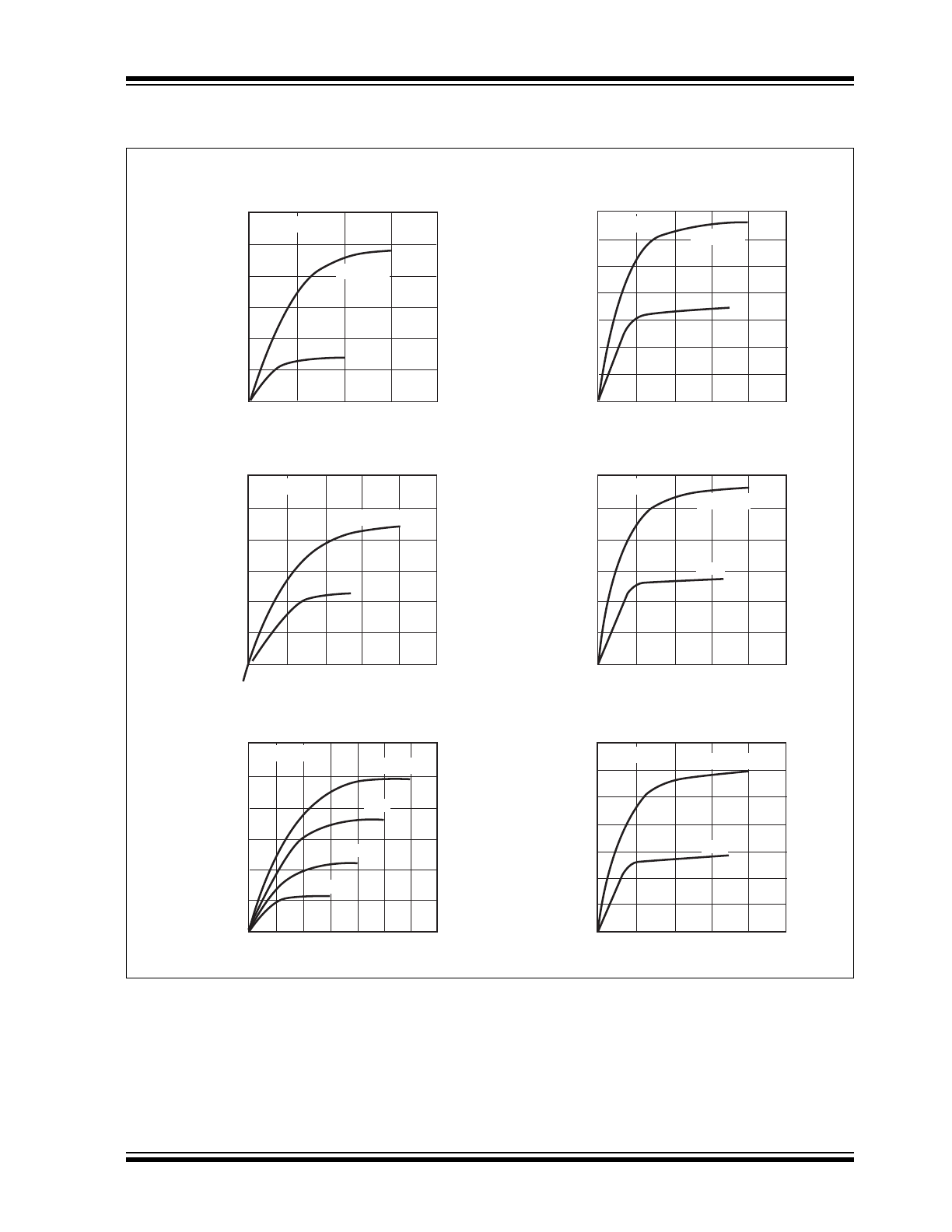
TYPICAL CHARACTERISTICS
Note:
The graphs and tables provided following this note are a statistical summary based on a limited number of
samples and are provided for informational purposes only. The performance characteristics listed herein are
not tested or guaranteed. In some graphs or tables, the data presented may be outside the specified
operating range (e.g., outside specified power supply range) and therefore outside the warranted range.
4.0
3.0
1.0
0.0
0
2
4
6
8
10
INPUT VOLTAGE V
IN
(V)
T
A
= 80°C
-30
°C
-30
°C
-30
°C
25
°C
2.0
TC51N1602
1. SUPPLY CURRENT VS. INPUT VOLTAGE
SUPPLY CURRENT I
SS
(µA)
4.0
3.0
1.0
0.0
0
2
4
6
8
10
INPUT VOLTAGE V
IN
(V)
2.0
TC51N2502
SUPPLY CURRENT I
SS
(µA)
25
°C
25
°C
4.0
3.0
1.0
0.0
0
2
4
6
8
10
INPUT VOLTAGE V
IN
(V)
2.0
TC51N3502
SUPPLY CURRENT I
SS
(µA)
T
A
= 80°C
T
A
= 80
°C
1.8
1.7
1.5
1.4
-40
-20
0
20
40
60
80
AMBIENT TEMPERATURE T
A
(
°C)
1.6
TC51N1602
2. THRESHOLD VOLTAGE, HYSTERESIS VOLTAGE VS. AMBIENT TEMPERATURE
THRESHOLD HYSTERESIS VOLTAGE V
DET
–
,V
HYST
80
V
HYST
2.8
2.7
2.5
2.4
2.3
-40
-20
0
20
40
60
AMBIENT TEMPERATURE T
A
(
°C)
2.6
TC51N2502
THRESHOLD HYSTERESIS VOLTAGE V
DET
–
,V
HYST
V
HYST
80
3.8
3.7
3.5
3.4
3.3
3.2
-40
-20
0
20
40
60
AMBIENT TEMPERATURE T
A
(
°C)
3.6
TC51N3502
THRESHOLD HYSTERESIS VOLTAGE V
DET
–
,V
HYST
V
DET
–
V
DET
–
V
DET
–
V
HYST
3.0
2.5
1.5
1.0
0.5
0.0
0
1
2
3
INPUT VOLTAGE V
IN
(V)
2.0
TC51N1602
3. OUTPUT VOLTAGE VS. INPUT VOLTAGE
OUTPUT VOLTAGE V
OUT
(V)
V
IN
– V
OUT
: 100k
T
A
= 30
°C
= 25
°C
= 80
°C
4
3
1
0
0
1
2
3
4
INPUT VOLTAGE V
IN
(V)
2
TC51N2502
OUTPUT VOLTAGE V
OUT
(V)
V
IN
– V
OUT
: 100k
T
A
= 30
°C
= 25
°C
= 80
°C
4
5
3
1
0
0
1
2
3
4
5
INPUT VOLTAGE V
IN
(V)
2
TC51N3502
OUTPUT VOLTAGE V
OUT
(V)
V
IN
– V
OUT
: 100k
T
A
= 30
°C
= 25
°C
= 80
°C
2002-2012 Microchip Technology Inc.
DS21429C-page 7
TC51
5.0
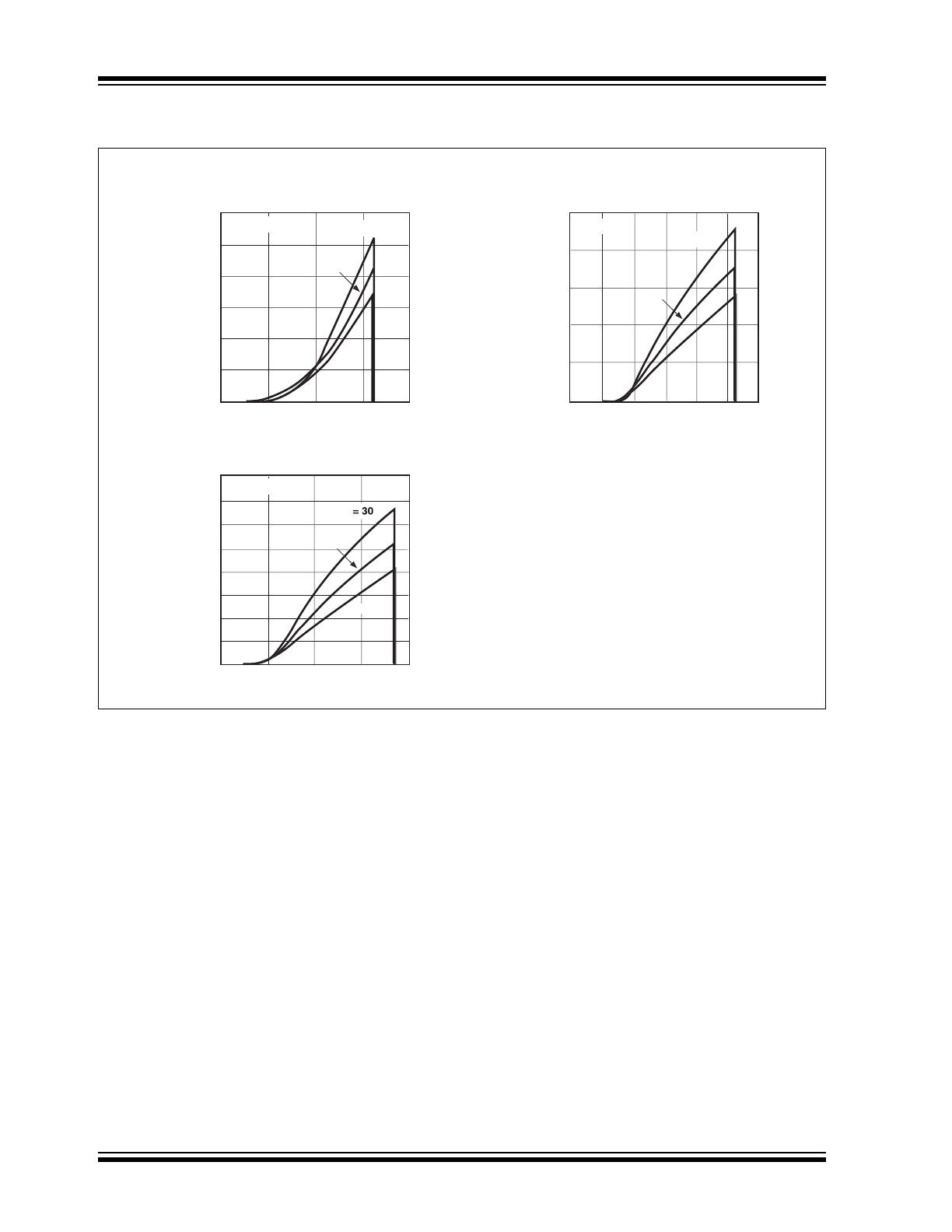
TYPICAL CHARACTERISTICS (CONTINUED)
15.0
12.5
7.5
5.0
2.5
0.0
0.0
0.5
1.0
1.5
2.0
V
DS
(V)
10.0
TC51N1602
4. OUTPUT CURRENT VS. V
DS
OUTPUT CURRENT I
OUT
(mA)
T
A
= 25°C
V
IN
= 1.5V
1.0V
1400
1200
800
600
400
200
0
0.2
0.4
0.6
0.8
1.0
V
DS
(V)
1000
TC51N1602
OUTPUT CURRENT I
OUT
(
µ
A)
T
A
= 25°C
V
IN
= 0.8V
0.7V
30
25
15
10
5
0
0.0
0.5
1.0
1.5
2.0
2.5
V
DS
(V)
20
TC51N2502
OUTPUT CURRENT I
OUT
(mA)
T
A
= 25°C
V
IN
= 2.0V
1.5V
1200
1000
600
400
200
0
0.0
0.2
0.4
0.6
0.8
1.0
V
DS
(V)
800
TC51N2502
OUTPUT CURRENT I
OUT
(
µ
A)
T
A
= 25°C
V
IN
= 0.8V
0.7V
60
50
30
20
10
0
0
0.5
1.0
1.5
2.0
2.5
3.0 3.5
V
DS
(V)
40
TC51N3502
OUTPUT CURRENT I
OUT
(mA)
T
A
= 25°C
V
IN
= 3.0V
V
IN
= 0.8V
2.5V
0.7V
2.0V
1.5V
1400
1200
800
600
400
200
0.0
0.2
0.4
0.6
0.8
1.0
V
DS
(V)
1000
TC51N3502
OUTPUT CURRENT I
OUT
(
µ
A)
T
A
= 25°C
TC51
DS21429C-page 8
2002-2012 Microchip Technology Inc.
5.0
TYPICAL CHARACTERISTICS (CONTINUED)
15.0
12.5
7.5
5.0
2.5
0.0
0.0
0.5
1.0
1.5
2.0
INPUT VOLTAGE V
IN
(V)
10.0
TC51N1602
5. OUTPUT CURRENT VS. INPUT VOLTAGE
OUTPUT CURRENT I
OUT
(mA)
V
DS
= 0.5V
T
A
= 30°C
25
°C
80
°C
80
°C
25
°C
25
°C
40
35
25
20
15
10
5
0
0
1.0
2.0
3.0
4.0
INPUT VOLTAGE V
IN
(V)
30
TC51N3502
OUTPUT CURRENT I
OUT
(mA)
25
20
15
10
5
0
0.0
0.5
1.0
1.5
2.0
2.5
3.0
INPUT VOLTAGE V
IN
(V)
TC51N2502
OUTPUT CURRENT I
OUT
(mA)
T
A
= 30
°C
V
DS
= 0.5V
V
DS
= 0.5V
80
°C
T
A
°C
2002-2012 Microchip Technology Inc.
DS21429C-page 9
TC51
6.0
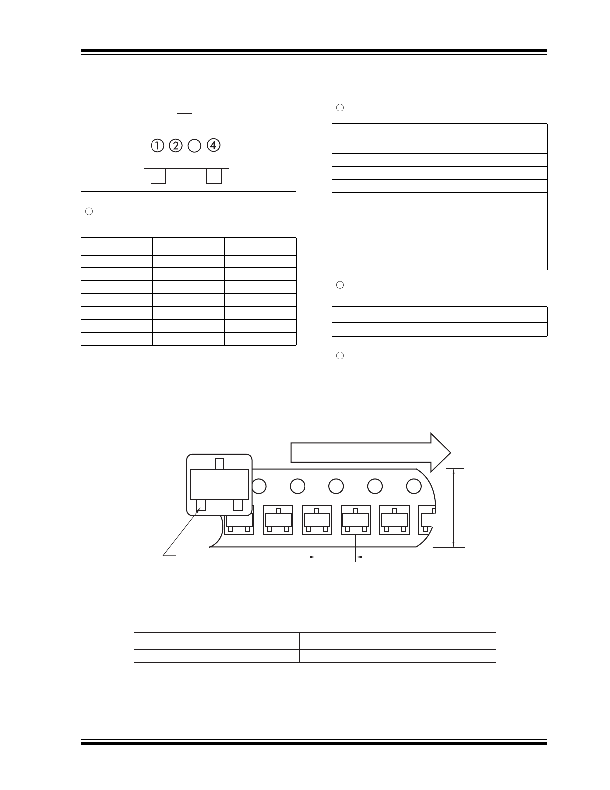
PACKAGING INFORMATION
6.1
Package Marking Information
6.2
Taping Form
Symbol
Output
Voltage
K
Nch
0.
L
Nch
1.
M
Nch
2.
N
Nch
3.
P
Nch
4.
R
Nch
5.
S
Nch
6.
3
1
represents N-channel indication and integer part
of output voltage
Symbol
Voltage
0
.0
1
.1
2
.2
3
.3
4
.4
5
.5
6
.6
7
.7
8
.8
9
.9
Symbol
Delay Time
5
50ms-200ms
2
represents first decimal of output voltage
3
represents delay time
4
represents assembly lot code
Component Taping Orientation for 3-Pin SOT-23A (EIAJ SC-59) Devices
Package
Carrier Width (W)
Pitch (P)
Part Per Full Reel
Reel Size
3-Pin SOT-23A
8 mm
4 mm
3000
7 in
Carrier Tape, Number of Components Per Reel and Reel Size
User Direction of Feed
Device
Marking
PIN 1
Standard Reel Component Orientation
for TR Suffix Device
(Mark Right Side Up)
W
P
TC51
DS21429C-page 10
2002-2012 Microchip Technology Inc.
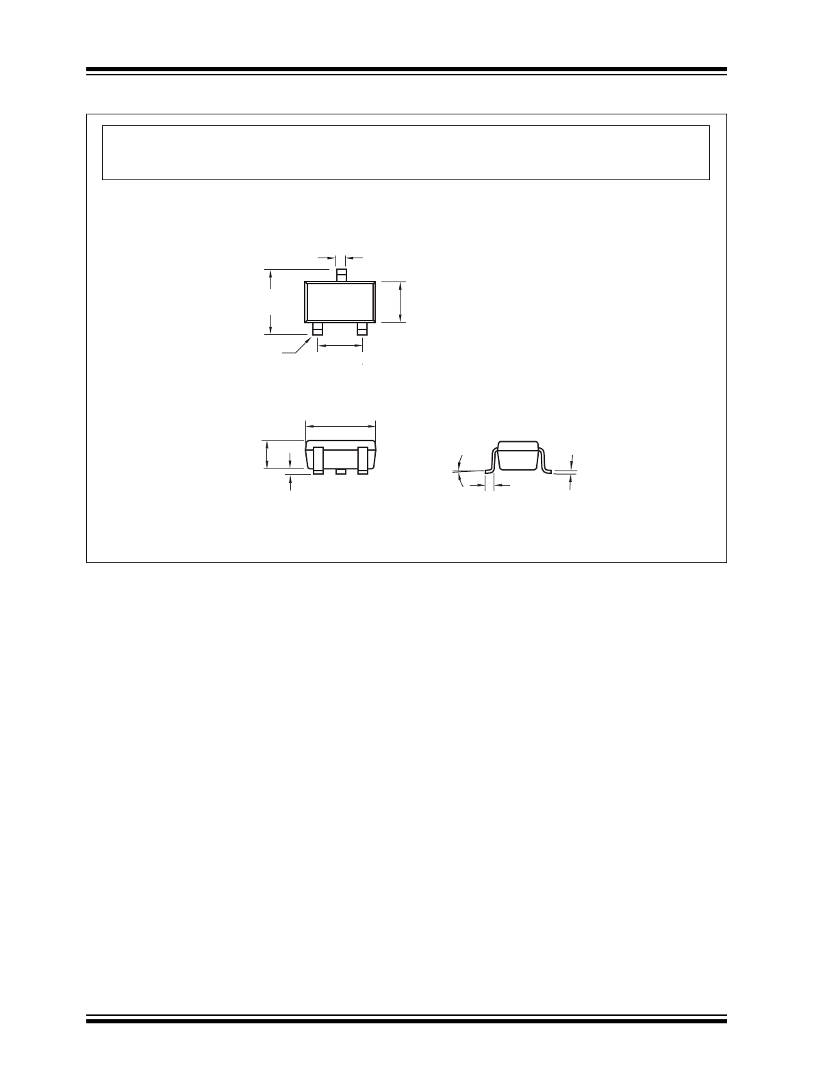
6.3
Package Dimensions
.071 (1.80)
.055 (1.40)
PIN 1
.118 (3.00)
.098 (2.50)
.020 (0.50)
.012 (0.30)
.075 (1.90)
REF.
.122 (3.10)
.106 (2.70)
.051 (1.30)
.035 (0.90)
.006 (0.15)
.000 (0.00)
.022 (0.55)
.014 (0.35)
10
° MAX.
.010 (0.25)
.004 (0.09)
SOT-23A-3
Dimensions: inches (mm)
Note:
For the most current package drawings, please see the Microchip Packaging Specification located
at http://www.microchip.com/packaging