
S E M I C O N D U C T O R
1
PRELIMINARY
August 1996
HIP7020
J1850 Bus Transceiver
I/O For Multiplex Wiring
Features
• J1850 Bus Transceiver I/O for MX Wiring
• 5V CMOS/TTL Logic Interface
• Current Controlled Transmitter Driver
• Controlled Rise/Fall Time of Bus Drive for Both
Voltage and Current
• Filtered Bus Input Receiver
• Ground Fault Tolerant for Bus Isolation
• Short Circuit and Over Temperature Protection
• Protection for Reverse Battery, Load Dump
and Latch-Up
•
±
9kV ESD Protection BUS OUT and BATTERY Pins
• -40
o
C to 125
o
C Operating Range
• Loop-Back Fault Detection Mode
• 4x (41.6kHz) Receive Speed
Description
The HIP7020 IC is an Integrated I/O Bus Transceiver
designed for the SAE Standard J1850 Class B Data Com-
munication Network Interface. The Bus transmits and
receives data on a single wire using a 10.4kHz VPWM (Vari-
able Pulse Width Modulated) signal. The HIP7020 is
intended as an I/O buffer interfacing to 5V CMOS logic and
is designed to operate directly from the 12V battery line of
an automobile. The normal Bus voltage swing capability is
from 0V to 7.75V at currents greater than 20mA.
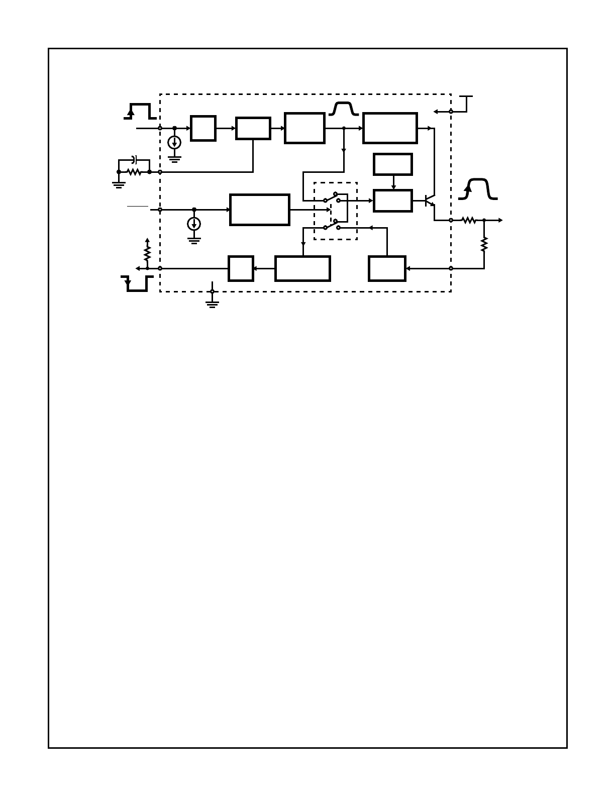
As shown in the Block Diagram, the Transmitter TX Input and
the Receiver RX Output of the Bus Transceiver Circuit inter-
face to the control logic. The TX input signal is wave shaped
for rise time, fall time and amplitude before it is converted
from voltage to current. The Wave Shaper with an external
programming resistor, R
S
controls the rise and fall time of
the BUS OUT output signal. The current source drive to the
Bus is voltage controlled by the Wave Shaped Voltage Refer-
ence to a maximum limit as specified for the J1850 Bus and
includes short-circuit current limiting.
The HIP7020 Receiver input is connected to the J1850 Bus
through an external resistor, R
F
and has a trip point at one-
half of the Bus signal voltage which is nominally 3.875V. The
Receiver input is filtered to remove high frequency Bus noise
by the external resistor and an internal capacitor. The bus
signal is output at the Receiver RX Output. The RX output is
active low and requires an external pull-up resistor returned
to the control logic V
CC
supply. This prevents power-up of
the control logic by the transceiver if V
CC
supply voltage is
removed.
The HIP7020 has a Loop-Back Enable Mode Switch to
return diagnostic information for the Bus Transceiver node.
For an active low or an open LB EN input, the Trans-
mit/Receive signals are internally “Looped-Back” to provide
a TX to RX return signal path independent of signals on the
Bus. A return path validation indicates proper action of the
Bus Transceiver apart from the J1850 Bus.
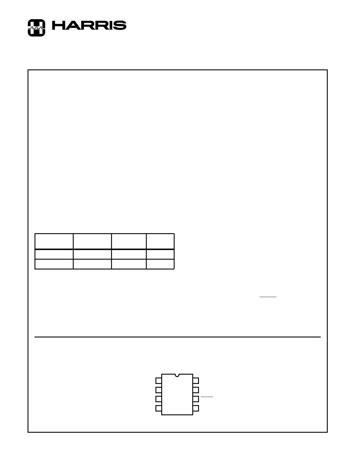
Pinout
HIP7020
(PDIP, SOIC)
TOP VIEW
Ordering Information
PART
NUMBER
TEMP.
RANGE (
o
C)
PACKAGE
PKG. NO.
HIP7020AB
-40 to 125
8 Ld SOIC
M8.15
HIP7020AP
-40 to 125
8 Ld PDIP
E8.3
BATT
TX
R/F TIME
RX
1
2
3
4
8
7
6
5
GND
BUS OUT
LB EN
BUS IN
CAUTION: These devices are sensitive to electrostatic discharge. Users should follow proper IC Handling Procedures.
Copyright
©
Harris Corporation 1996
File Number
3642.2
2
Block Diagram
TX
WAVE
SHAPER
WAVE
VOLT. REF
SHAPED
VOLTAGE TO
CONVERTER
FILTER
BUS RCVR &
VOLT. COMP.
RX
TX
RX
BUS OUT
I
STX
GND
BUS IN
R
S
R
F
BATT
V
CC
CURRENT
V
REF
LOOP-BACK
MODE SW
†
OVER-
V+
HIP7020
Q1
I
SLB
LB EN
R
D
DIAGNOSTIC
BUF
BUF
LEVEL
SHIFTER
I
BO
TEMP SW
†
SWITCH SHOWN IN
LOOP-BACK MODE
V
BO
R
E
R/F TIME
C
2
R/F
TIME
HIP7020
3
Absolute Maximum Ratings
Thermal Information
Supply Voltage, V
BATT
. . . . . . . . . . . . . . . . . . . . . . . . . -20V to +24V
Short Term Supply Voltage, V
BATT
, 1s Max. (Note 1) . . . . . . . +35V
J1850 Bus Input Voltage, V
BUS IN
. . . . . . . . . . . . . . . . . . . . . .
±
20V
J1850 Bus Load Current, I
BO
. . . . . . . . . . . . . . . . . . . . .Self-Limiting
TX Logic Input Voltage . . . . . . . . . . . . . . . . . . . . . . GND -0.3V to 7V
RX Logic Output Current . . . . . . . . . . . . . . . . . . . . . . . . . . . . . 5mA
Load Dump (Note 1) . . . . . . . . . . . . . . . . . . . . . . . . . . . . . . . . . . 40V
BUS Transient Susceptibility . . . . . . . . . . . . . . . . . . . . . . . (Note 2)
ESD:
BUS OUT, BATTERY Pins, (Air Gap, Note 3) . . . . . .
±
9kV
BUS OUT, BATTERY Pins, (Direct, Note 3)
. . . . . . . ±
4.5kV
All Other Pins (Direct, Note 3) . . . . . . . . . . . . . . . . . .
±
2kV
Operating Conditions
Operating Temperature Range . . . . . . . . . . . . . . . . . -40
o
C to 125
o
C
Thermal Resistance (Typical)
θ
JA
(
o
C/W)
PDIP Package . . . . . . . . . . . . . . . . . . . . . . . . . . . . .
120
SOIC Package . . . . . . . . . . . . . . . . . . . . . . . . . . . . .
160
Maximum Junction Temperature . . . . . . . . . . . . . . . . . . . . . . . 150
o
C
Maximum Storage Temperature Range . . . . . . . . . .-40
o
C to 150
o
C
Maximum Lead Temperature (Soldering 10s) . . . . . . . . . . . . . 265
o
C
CAUTION: Stresses above those listed in “Absolute Maximum Ratings” may cause permanent damage to the device. This is a stress only rating and operation
of the device at these or any other conditions above those indicated in the operational sections of this specification is not implied.
NOTES:
1. Fault capability of the J1850 Bus Transceiver includes reverse battery, load dump and latch-up tolerance to
±
200mA on any terminal. The
Short Term Power Supply Voltage capability is 35V for a maximum of 1s. Continued operation at this voltage may cause thermal shutdown.
2. Transient Susceptibility Bus and Battery Pins Per SAE J1113, Aug 1987, Figures 7 Test Pulses 1, 2, 3A and 3B at -50V, +100V and
±
200V
respectively.
3. ESD Conditions - SAE J1113; Aug 1987.
BUS OUT & BATTERY Pins: Air Gap and Direct Contact Discharge; R = 2k
Ω
, C = 150pF
All Other Pins: Direct Contact Discharge; R = 1.5k
Ω
, C = 100pF
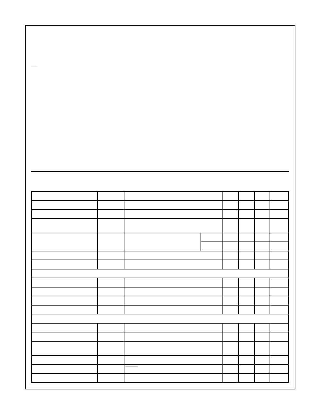
Electrical Specifications
9.5V
≤
V
BATT
≤
16V; R
S
= 56.2k
Ω ±
1%; All voltages are measured with respect to ground and the
T
A
Range of -40
o
C to 125
o
C shall not be exceeded during test unless otherwise specified. For test detail,
refer to the Block Diagram, Figures 1 and 2 Test Circuits and Figures 3 and 4 Waveforms.
PARAMETER
SYMBOL
TEST CONDITIONS
MIN
TYP
MAX
UNITS
Idle Supply Current
I
BATT
No Bus Signal; V
BATT
= 12.6V; V
TX
Low
90
200
350
µ
A
Operating Voltage Range
V
BATT
(Note 4)
6
-
24
V
Supply Current,
BUS OUT Short to GND
I
BATT(SG)
BUS OUT Short to GND, V
TX
High
20
-
50
mA
Supply Current,
BUS OUT Short to BATT
I
BATT(SB)
BUS OUT to V
BATT
; I
BO
= 0 mA
V
TX
High
2
-
8
mA
V
TX
Low
90
-
350
µ
A
Thermal Shutdown Temperature
T
SD
(Note 5)
150
-
170
o
C
Thermal Shutdown Hysteresis
T
SDHYS
(Note 5)
5
10
15
o
C
TX CMOS/TTL INPUT WITH/PULL DOWN
Input Bias Current, TX
I
TX
V
TX
= 7V; (Note 6)
20
-
35
µ
A
Input Low Voltage
V
IL
-
-
0.8
V
Input High Voltage
V
IH
2.0
-
-
V
Input Capacitance
C
TX
2
-
5
pF
BUS OUT
BUS OUT High Voltage
V
BOH
Bus Load, R
BS
= 500
Ω
to 1.5k
Ω
; V
TX
High
6.8
-
8
V
BUS OUT Low Voltage
V
BOL
Bus Load, R
BS
= 1.5k
Ω
; V
TX
Low
-
-
0.1
V
BUS OUT Voltage, Low Battery
V
BOH(PSL)
6V
<
V
BATT
<
8.5V; V
TX
High
V
BATT
- 1.3
-
8
V
Source Current, Bus Low
I
BO_LIMIT
-20V
≤
V
BUS OUT
<
V
BOH
; V
TX
High
-20
-
-42
mA
BUS OUT During LOOPBACK
V
LOOPBACK
LB EN Low, V
TX
High
-
-
1
V
Bus Emissions Voltage Output
V
dB_LIMIT
-60
-
-
dBV
HIP7020
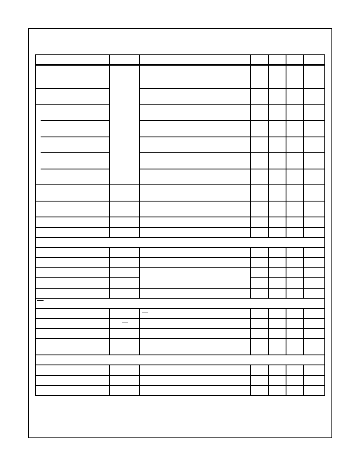
4
BUS OUT Leakage Currents
I
BO_LEAK
Battery Low/Off1
0V
≤
V
BUS OUT
≤
20V; 0V
≤
V
BATT
≤
0.8V;
-0.3
≤
V
TX
≤
7V
-10
-
10
µ
A
Battery Low/Off2
-20V
≤
V
BUS OUT
≤
0V; 0V
≤
V
BATT
≤
0.8V;
-0.3
≤
V
TX
≤
7V
-10
-
100
µ
A
Bus High
V
BOH
<
V
BUS OUT
≤
20V; 6V
≤
V
BATT
≤
16V;
2
≤
V
TX
≤
7V
-10
-
10
µ
A
TX Low1
0V
≤
V
BUS OUT
≤
20V; 6V
≤
V
BATT
≤
16V;
-0.3
≤
V
TX
≤
0.8V
-10
-
10
µ
A
TX Low2
-20V
≤
V
BUS OUT
<
0V; 9.5V
≤
V
BATT
≤
16V;
-0.3
≤
V
TX
≤
0.8V
-10
-
100
µ
A
With Loss of Ground1 (Note 10)
V
GND
≤
V
BUS OUT
<
20V; 0V
≤
V
BATT
≤
16V;
-0.3
≤
V
TX
≤
7V
-10
-
10
µ
A
With Loss of Ground2 (Note 10)
-20V
≤
V
BUS OUT
≤
V
GND
; 0V
≤
V
BATT
≤
16V;
-0.3
≤
V
TX
≤
7V
-10
-
100
µ
A
TX to BUS OUT Propagation
Delays
t
DTXHBO
,
t
DTXLBO
R
BS
= 11k
Ω
; C
BS
= 330pF; R
S
= 56.2k
Ω
;
V
BUS OUT
= 3.875V (Note 7)
10
16
23
µ
s
BUS OUT Transition Times,
Rise and Fall
t
R
, t
F
R
BS
= 500
Ω
; C
BS
= 470pF; R
S
= 56.2k
Ω
; Measured
on BUS OUT between 1.5V and 6.25V (Note 7)
13
16
18
µ
s
BUS OUT Noise Rejection
N
R
f
R
= 30Hz to 250kHz; V
BATT
to BUS OUT
20
-
-
dB
BUS OUT RF Isolation
N
I
f
I
= 0.25MHz to 200MHz; V
BATT
to BUS OUT
20
-
-
dB
BUS IN
Input Threshold Voltage
V
BIH
3.65
-
4.1
V
Input Bias Current
I
BIN
-20V
≤
V
BUS IN
≤
20V
-5
-
5
µ
A
Input Resistance
R
BIN
-20V
≤
V
BUS IN
≤
20V; 0V
≤
V
BATT
≤
16V;
V
TX
High or Low
200
-
-
k
Ω
Input Capacitance
C
BIN
10
-
20
pF
Filter Bandwidth
f
BW
(3dB)
Measure with Ext. Series Resistor, R
F
=15k
Ω
500
750
1000
kHz
RX OUTPUT
Output Voltage, Low
V
IL
I
RX
= 1.6mA
0.01
-
0.4
V
Output Current
I
RX
V
RX
= 5V (Note 9)
2
5
8
mA
Output Leakage Current
I
RX(LK)
V
RX
= 5V, R
D
= 10k
Ω
; V
BUSIN
Low
-10
-
10
µ
A
Receive Propagation Delay
t
DRXON
,
t
DRXOFF
Measured from BUS IN Threshold Voltage
1
-
4
µ
s
LB EN CMOS/TTL INPUT WITH/PULL DOWN
Input Low Voltage
V
IL
-
-
0.8
V
Input High Voltage
V
IH
2.0
-
-
V
Input Bias Current
I
LB
V
LB
= 7V; (Note 8)
4
-
10
µ
A
Electrical Specifications
9.5V
≤
V
BATT
≤
16V; R
S
= 56.2k
Ω ±
1%; All voltages are measured with respect to ground and the
T
A
Range of -40
o
C to 125
o
C shall not be exceeded during test unless otherwise specified. For test detail,
refer to the Block Diagram, Figures 1 and 2 Test Circuits and Figures 3 and 4 Waveforms. (Continued)
PARAMETER
SYMBOL
TEST CONDITIONS
MIN
TYP
MAX
UNITS
HIP7020
5
TX To RX Turn ON, OFF;
Delay In Loop-Back Mode
t
DLBON
,
t
DLBOFF
V
LB
Low; Toggle TX; Meas. RX
13
-
25
µ
s
LB EN Turn ON, OFF;
TX to BUS OUT
t
D(LH)
,
t
D(HL)
V
TX
High; Toggle LB EN; Meas. BUS OUT
1
-
10
µ
s
NOTES:
4. In the operating voltage range from 6V to 8.5V the BUS OUT, V
BOH
is limited by the low power supply. In the operating voltage range
from 16V to 24V the maximum bus load is limited by the package power dissipation ratings.
5. Over-temperature shutdown with hysteresis is incorporated to protect the IC under system failure conditions.
6. Measured Current into the TX terminal is determined by Pull-Down Current Sink.
7. Propagation Delay limits are measured at the 3.875V level on BUS OUT. Rise and Fall Times are measured between 1.5V and 6.25V on
the BUS OUT terminal.
8. Measured Current into the LB EN terminal is determined by Pull-Down Current Sink.
9. The I
RX
Output Current test parameter defines Short Circuit protection limits.
10. Loss of Ground refers to loss of module (node) Ground which results in a voltage between the Battery and IC Ground of less than 0.8V.
For voltage between Battery and Ground above 0.8V, the Transceiver Bus Output may become active. The module circuit in Figure 1 is
used to measure the Loss of Ground leakage.
11. Unless otherwise noted, all Electrical Specification test conditions are as shown in Figure 1.
Electrical Specifications
9.5V
≤
V
BATT
≤
16V; R
S
= 56.2k
Ω ±
1%; All voltages are measured with respect to ground and the
T
A
Range of -40
o
C to 125
o
C shall not be exceeded during test unless otherwise specified. For test detail,
refer to the Block Diagram, Figures 1 and 2 Test Circuits and Figures 3 and 4 Waveforms. (Continued)
PARAMETER
SYMBOL
TEST CONDITIONS
MIN
TYP
MAX
UNITS
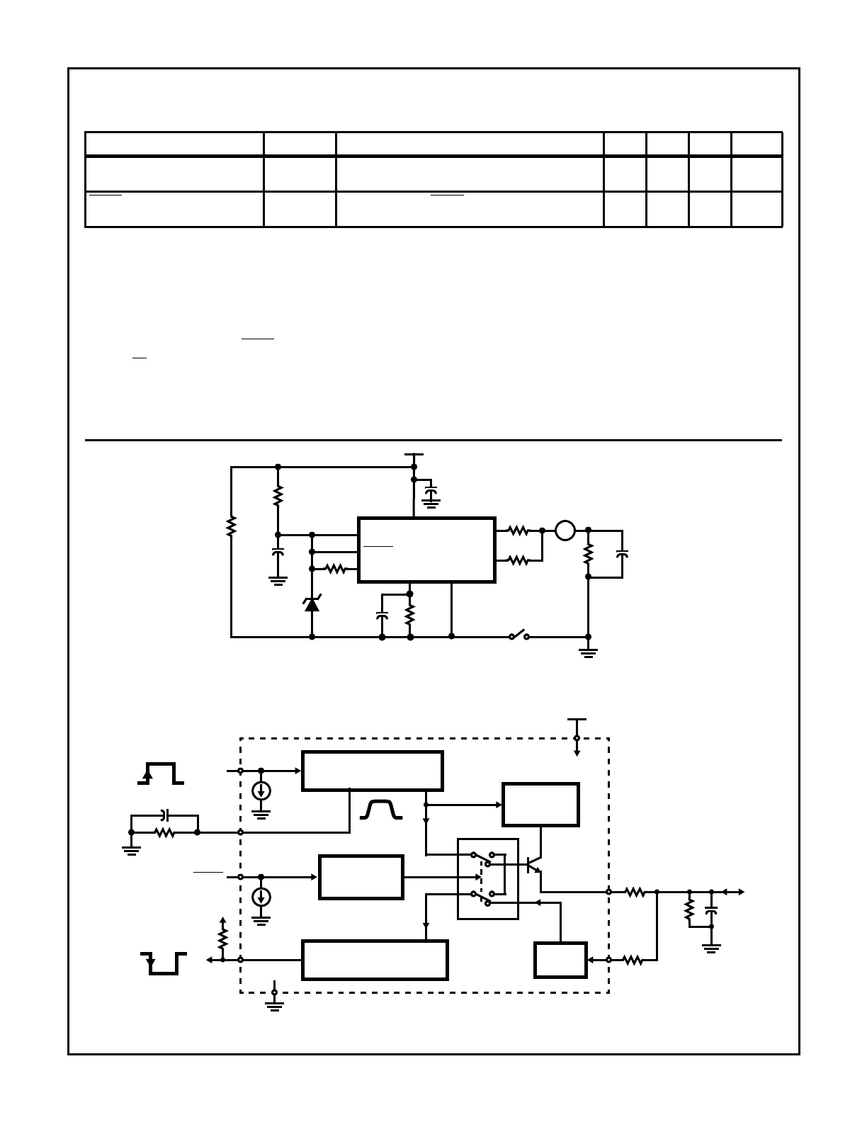
FIGURE 4. LOSS OF GROUND LEAKAGE TEST CIRCUIT
FIGURE 5. ELECTRICAL SPECIFICATION TEST CIRCUIT
0.1
µ
F
BUS OUT
BUS IN
BATT
GND
RX
TX
R/F
LB EN
0.01
µ
F
V
BATT
56.2K
10
15K
500
0.01
µ
F
SW
10K
5.1V
0.1
µ
F
100
510
µ
A
Test Circuits
TRANSMIT WAVEFORM
PROCESSING/SHAPING
VOLTAGE TO
CONVERTER
FILTER
TX
RX
BUS OUT
I
STX
GND
BUS IN
R
S
R
F
BATT
5V
CURRENT
V
REF
LOOP-BACK
MODE SW
†
Q1
I
SLB
LB EN
R
D
DIAGNOSTIC
I
BO
†
SWITCH SHOWN IN
LOOP-BACK MODE
V
BO
R
E
R/F TIME
C
2
R/F
TIME
V
TX
LOW = 0V
V
TX
HIGH = 5V
0.01
µ
F
56.2k
±
1%
5k
BUS RECEIVER AND
VOLTAGE COMPARATOR
15k
10
R
BS
= 500 to 1500
τ
= R
BS
C
BS
≅
5
µ
s
V
BATT
C
BS
R
BS
HIP7020

6
HIP7020 Signal Interface
The HIP7020 is a member of the Harris family of low cost
multiplexed wiring ICs. As a Bus Transceiver IC, it interfaces
the module and system control logic to the vehicle signal bus
wiring. The integrated functions of the Bus Transceiver serve
as an interface for a “Class B” multiplexed communications
network. The TX digital interface is designed to accept
CMOS/TTL logic levels and convert them to the appropriate
J1850 analog serial data levels. This is accomplished using
an internally generated reference waveform and voltage
driver with a controlled current source to supply an analog
signal output to the J1850 bus load of 500
Ω
(typical).
Because of the special wave shaping used to control the
J1850 bus waveform, it is regarded as an analog signal.
In the receive mode the incoming bus analog signals are input
to the receiver at the BUS IN terminal. The bus data is
converted to logic information by comparing it to an on-chip
reference voltage. The received signal is provided as digital
output from an open collector transistor driver at the
RX output.
In the transmit mode a CMOS/TTL digital signal is received
at the TX input. It is then rise and fall time controlled, wave
shaped and level adjusted. A voltage controlled current
driver circuit transmits the signal from the BUS OUT terminal
to the J1850 Bus with current limiting protection.
Functional Blocks
The Bus Transceiver IC functional blocks, as shown in the
Block Diagram, are as follows:
TX BUF (Transmit Input Buffer Interface)
The TX Buffer input function is a data interface to the wave-
shaper reference circuit. The CMOS/TTL logic levels to be
transmitted are input to the TX pin.
Waveshaper Circuit
This stage defines the transitions of high and low signal levels
to provide a uniform rise and fall time. The input signal to the
Waveshaper is the TX Buffer output and is an active high
signal. In the Waveshaper the Transmit signal is amplified and
compared to an internal reference voltage. The Waveshaper
also provides waveform corner shaping on both the positive
and negative going transitions. The rise and fall time of the
serial waveform is set by the Waveshaper circuit and an
external programming resistor, R
S
that sets an internal
current reference for control of the rise and fall slopes of
the waveform.
Wave Shaped Voltage Reference Drive, V
REF
The Wave Shaped Voltage Reference circuit sets a scaled
analog signal level and maintains a constant peak-to-peak
voltage during worst case battery voltage conditions, includ-
ing cold cranking. The analog signal from the Wave Shaped
Voltage Reference circuit drives the Voltage-to-Current Con-
verter and a Level Shifter Interface to the bus driver transis-
tor, Q1. The Voltage-to-Current Converter, in addition to the
waveform leveling, helps to preserve low RFI and drive
integrity. The edges of the wave shaped waveform, V
REF
have well defined rise and fall times and the knees of the
waveform are smooth and rounded as signal conditioning to
reduce RFI.
Voltage-to-Current Converter
The Voltage-to-Current Converter determines the maximum
current to be sourced out to the J1850 bus and is designed
to source current proportional to the input signal from the
Wave Shaped Voltage Reference, V
REF
. The output of the
Voltage-to-Current Converter maintains drive integrity of the
V
REF
waveform without the use of feedback.
A small quiescent current source is supplied to maintain a
fixed minimum for each bus node. This precisely fixes the
quiescent current at low input signal drive to the Voltage-to-
Current Converter.
Voltage Controlled Current Driver, Q1
The Voltage Controlled Current Driver, Q1, controls the
amount of current sourced out to the J1850 Bus. The Wave
Shaped Voltage Reference, V
REF
, drives the base of Q1 and
the Voltage-to-Current Converter drives the collector of Q1.
Both voltage and current determine the drive level which is
supplied to the bus. When the Bus voltage is below the level
determined by the Voltage Reference, V
REF
, the Voltage
Controlled Current Driver allows more current to be sourced
out to the J1850 Bus. Voltage drive may increase as needed
until the Bus voltage and the Voltage Reference match or
until the maximum current limit is reached, as set by the Volt-
age-to-Current Converter. When the Bus voltage is above
the Voltage Reference the Voltage Controlled Current Drive
to the J1850 Bus is decreased. Decreasing correction
occurs until the Bus voltage and the Voltage Reference
match or until zero current is being sourced.
Filter, Bus Receiver and Voltage Comparator
The Filter limits the high frequency bandwidth by external
resistor, R
F
, and the input capacitance of the Filter Block.
The on-chip Filter network and the external resistor, R
F
,
form a low pass filter to reject high frequency noise that may
be present on the bus. Resistor, R
F
, also provides isolation
protection from transients. The analog bus signal is passed
to the Bus Receiver and Voltage Comparator which deter-
mine when the bus is high or low as referenced to half the
nominal bus voltage at the BUS IN pin.
RX BUF (Receiver Output Buffer Interface)
The RX BUF function is a buffer for the logic output as deter-
mined by the Bus Receiver and Voltage Comparator. An
open collector transistor supplies current switched output to
an external load resistor, R
D
. BUS IN data is converted to
serial CMOS/TTL logic data which is output at the RX pin of
the HIP7020. Resistor, R
D
, is biased from the digital 5V sup-
ply for optimum output drive levels to the logic circuits and to
avoid power-up of the digital parts via the transceiver.
HIP7020

7
Thermal Shutdown
Over-temperature shutdown with hysteresis is incorporated to
protect the IC under system failure conditions. Temperature
is sensed at the transistor, Q1. Thermal shutdown will occur
when the temperature of the chip reaches +150
o
C (mini-
mum) and will latch-off the HIP7020 Transmitter operation. A
reset occurs on the first positive edge transition of the next
transmit data bit after ~10
o
C decrease in chip temperature.
Hysteresis in the thermal shutdown threshold is necessary
to allow the temperature to decrease to a safe operating
temperature, typically less than +140
o
C.
Diagnostic Loop-Back Mode Switch
The HIP7020 has an active low Loop-Back Enabled Mode
Switch which controls an internal signal path to provide diag-
nostic information. When Enabled, the Transmit/Receive sig-
nals are internally “Looped-Back” independent of the signal
conditions on the J1850 Bus. A return path validation indi-
cates proper action of the Bus Transceiver apart from the
J1850 Bus. In the Loop-Back Mode, the transistor, Q1 output
is forced low, preventing the output from sourcing current to
the bus. Loop-Back is not affected by thermal shutdown.
NOTE: The Block Diagram switch position is shown for Loop-Back
operation. A pull-down at the LB EN input forces an active low Loop-
Back mode as the default position when no connection is applied.
Operational Description
Bus Output Signal
The BUS OUT output drive from the HIP7020 conforms to
the SAE Standard J1850 Class B Data Communication
Network Interface document specifications. It meets these
requirements without oscillation, glitches or overshoots. The
digital signal to be transmitted is wave shaped and amplitude
controlled to produce an analog serial data waveform with
precisely defined rise and fall edges. Operational capability
covers a wide range of bus load resistances, capacitances
and characteristic impedance while complying with the arbi-
tration requirements of the Bus. Transient noise interference
on the bus is minimized by the bus interface filtering and
control circuitry of the Bus Transceiver IC.
High Current may exist during noise interference and bus
arbitration conditions on the bus. To limit instantaneous cur-
rent direction change and minimize the level of fluctuating
current caused by these conditions, a series resistance is
used in the bus output of the HIP7020. (See Figure 5). A
small resistor, R
E
, from the BUS OUT pin to the bus module
connection forces a distribution of bus current between
transmitting modules and provides load stability to the IC.
The HIP7020 maintains a uniform and consistent bus
waveform having specific transition times and propagation
delays to preserve a J1850 analog data stream. Transmitted
bus data is encoded by a HIP7010 Byte Level IO or HIP7030
J1850 microcontroller, (see Figure 5) where “1s” and “0s”
are defined by the length of time in which the bus voltage is
high or low. Precise waveform control is necessary for a
receiving node to accurately decode the difference between
“1s” and “0s” by the time duration of high levels and low
levels on the bus. In order to retain bus data integrity, digital
information to be transmitted on the bus is wave shaped and
amplitude controlled in the Bus Transceiver. The transmitted
signal output to the J1850 Bus is a waveform with uniform
edge control and precisely defined voltage levels.
Bus Current and Voltage Control
The Bus Transceiver has a Wave Shaped Voltage Reference
which controls both the Voltage-to-Current Converter and
the Bus Voltage Driver, Q1. The Voltage-to-Current Con-
verter supplies a limited current feed to the collector of Q1.
Together this provides the function of a Voltage Controlled
Current Driver which controls the bus voltage drive level
while supplying limited current to drive the bus load.
Wave Shaped Voltage Reference, V
REF
The output of the Wave Shaped Voltage Reference is a uni-
form signal which is a scaled waveform of the desired bus
signal and is shown as V
REF
in Block Diagram. This signal
controls the output current driver and is the input to the Volt-
age-to-Current Converter. The internal reference voltage,
V
REF
is isolated from the J1850 Bus and is totally unaffected
by the signal conditions on the bus. This isolation provides
superior Bus stability in the vehicle environment. The bus
drive control interface maintains the integrity of the V
REF
waveform supplied to the bus. This is done without feedback
control which is inherently susceptible to oscillation.
Voltage-to-Current Converter
The Voltage-to-Current Converter generates a current, I
BO
which is proportional to the Wave Shaped Voltage Reference
magnitude and waveshape. This is the maximum current
that can be supplied to the bus and is limited to a value of
30mA typical.
Voltage Controller Current Driver
The Voltage Controller Current Driver, Q1, is the device
which controls the amount of the available current which will
be sourced out to the bus as determined by the Voltage Ref-
erence and allowed by the Voltage-to-Current Converter.
When the Bus voltage is below the Voltage Reference, Q1
allows more current to be sourced out to the J1850 Bus; until
the Bus voltage and the Voltage Reference match or until the
maximum current limit is reached as set by the Voltage-to-
Current Converter.
When the Bus voltage is above the Voltage Reference, Q1
allows less current sourced out to the J1850 Bus; until the
Bus voltage and the Voltage Reference match or until zero
current is being sourced from Q1.
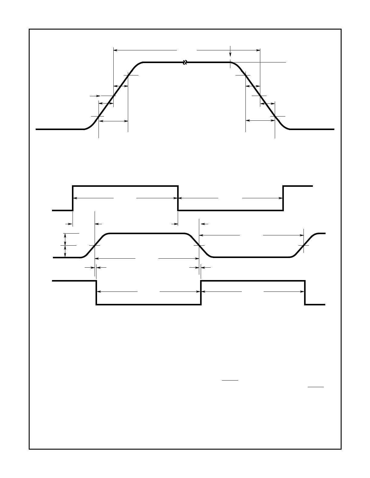
Bus Output Waveform
The bus output waveform shown in Figure 3 is controlled by
the internal Wave Shaper and has a tightly controlled rise
and fall time with rounded corners. The rise/fall times, t
R
and
t
F
, are defined between V
BOL
and V
BOH
.
HIP7020
8
Constant Propagation Time Delay
There is a constant propagation time delay from TX signal
going high or low to the BUS OUT signal (measured at
3.875V). The propagation time delay signals are shown in
Figure 4. The timing to reach the 50% voltage level of the
bus signal from the start of TX input going high is t
DTXHBO
.
The propagation time delay from the start of TX input going
low is t
DTXLBO
.
The BUS IN input signals, as shown in Figure 4, are charac-
terized by the V
BIH
and V
BIL
specifications which include
hysteresis. There is a constant propagation delay for the Bus
to RX receive channel of the Bus Transceiver. The received
propagation delay times are t
DRXON
and T
DRXOFF
as mea-
sured in reference to the 50% voltage level on the rising or
falling edge of the BUS IN input signal to the rising or falling
edge of the RX output signal.
Low Pass Filter Input
The bus input has an on-chip input filter to strip off the
unwanted incoming high frequency noise. The 3dB point of
this filter is nominally 750kHz.
Diagnostic Bus-isolated Loop-back
An on-chip Bus-Isolated Diagnostic Loop-Back function is con-
trolled by the LB EN pin. The Loop-Back function is a mode
switch that is enabled by placing a logic low on the LB EN pin.
When activated, the signal flow is cross-switched to open the
Bus Receive Input and connect the Voltage Reference,
V
REF
output to the input of the Bus Receiver. This “Loops-
Back” the TX signal to the RX output while maintaining isola-
tion from the signal on the J1850 Bus. When the Loop-Back
is enabled, diagnostic trouble shooting can be done at each
individual node regardless of fault conditions on the bus.
NOTE:
Refer to SAE J1850, Table 5 for definition of Tv_ time durations definitions. i.e. By Definition a Short pulse = Tv1: t
TX(NOM)
= t
RX(NOM)
= 64
µ
s.
FIGURE 6. J1850 BUS WAVEFORM
FIGURE 7. PROPAGATION TIME DELAYS
50% = 3.875V
50%
100% = 7.75V
1.5V
V
BOH(MIN)
V
BOL(MAX)
8
µ
s
16
µ
s
8
µ
s
t
F
= t
T
6.25V
8
µ
s
16
µ
s
t
R
= t
T
TX GOES
LOW
Tv_
8
µ
s
(NOTE)
TRANSMIT
J1850
RECEIVE
50% VOLT LEVEL
50% VOLT LEVEL
t
DTXHBO
t
DTXLBO
t
DRXON
t
DRXOFF
3.875V
3.875V
Tv_
BUS
(TX)
Tv_
Tv_
Tv_
Tv_
Tv_
(RX)
HIP7020
9
Thermal Shut Down Protection
On-chip Thermal Shutdown Protection is designed to shut-
down source drive to the J1850 bus and protect the Bus
Transceiver IC output. The temperature shutdown threshold is
set to protect the absolute maximum junction temperature of
the chip and is nominally set for +160
o
C with 10
o
C of hystere-
sis. Thermal shutdown may occur when overload conditions
exist on the bus. (See Function Blocks - Thermal Shutdown)
Package Pinout
BATT
The BATT pin is connected directly to the vehicle Battery
(Ignition) line. The Battery supply connection (V
BATT
) pro-
vides voltage for all on-chip functions, including the voltage
reference. As such, the BATT input is designed to withstand
transient power supply conditions.
TRANSMIT (TX)
The TRANSMIT pin will accept standard CMOS/TTL logic
level input data. Logic level data is input at the TRANSMIT
(TX) pin in a serial format, such as provided by a Harris
HIP7030A2 J1850 Controller, and is output on the J1850
Bus at the BUS OUT pin. The TX input has an active pull
down current sink to insure that a logic level low will be main-
tained when no signal drive is present.
RECEIVE (RX)
The RX pin is the output for J1850 Bus data and interfaces
to an open collector transistor output driver. The RX digital
data output is inverted from the analog bus data input at the
BUSIN pin. The data from the RX pin is output to a Harris
HIP7010 Byte Level I/O or a HIP7030A2 Protocol Microcon-
troller IC where the 10.4Kbps VPWM messages from the
J1850 network are decoded.
GROUND
This is the HIP7020 Bus Transceiver IC ground reference for
all the signals which interface to the control logic and the
J1850 bus. It is also the ground return path for the BATTERY
power supply to IC.
R/F TIME
The R/F (Rise/Fall) Time pin connects the external resistor,
R
S
, from the wave shaped voltage reference to ground. The
Rise and Fall Time is controlled by the transition slope of the
signal waveform. The resistor, R
S
, sets an internal current
reference to control the rise and fall slope.
BUS IN
The BUS IN pin is the receive input of the SAE J1850 Bus
signal. It receives the 10.4kHz VPWM (Variable pulse width
modulated) data from the single wire analog serial bus
through an external Resistor, R
F
.
BUS OUT
The BUS OUT pin transmits the SAE J1850 10.4kHz VPWM
(Variable Pulse Width Modulated) data to the serial bus.
Data is transmitted to the serial J1850 bus with the same
polarity as the TX input signal.
LB EN
The LB EN Loop-Back Enable pin controls the Diagnostic
Loop-Back Mode Switch function. A logic low on the LB EN
pin connects the output of the Wave Shaped Voltage Refer-
ence to the Bus Receiver and Voltage Comparator while dis-
connecting the filtered input of J1850 Bus. This feature
provides the means to trouble shoot system problems.
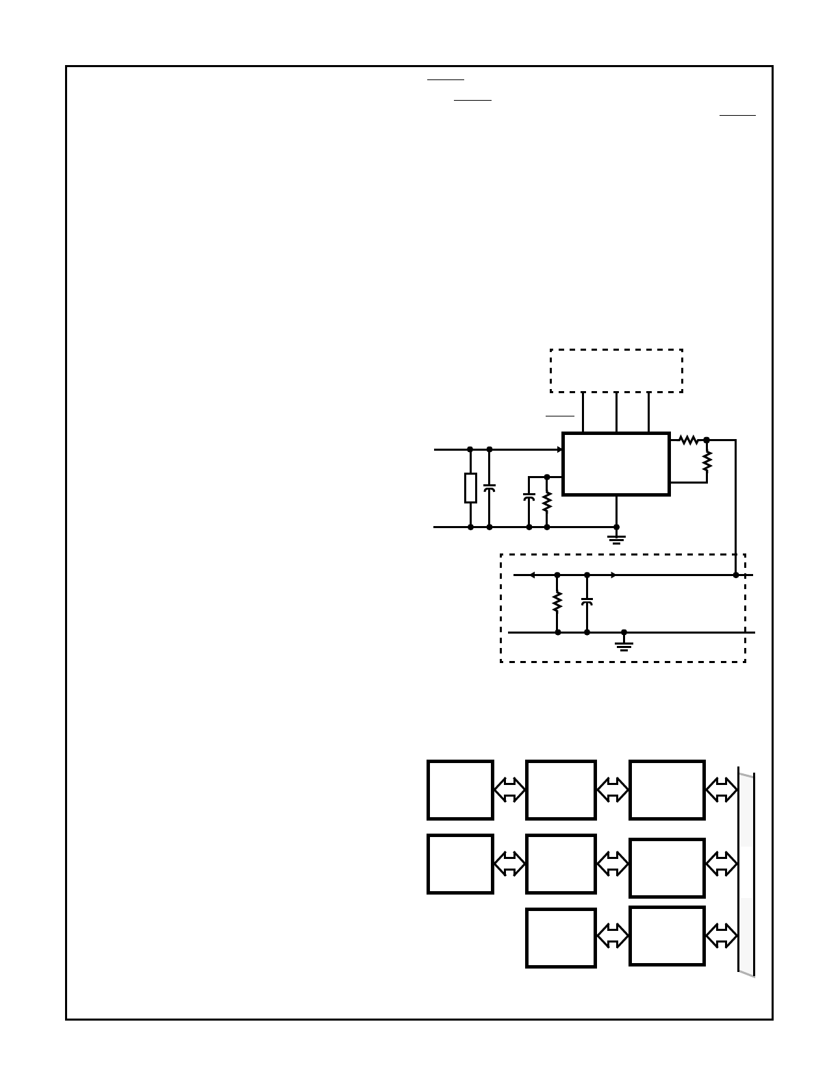
Test/Application Circuit
The circuit of Figure 5 illustrates the essential elements of
the J1850 Bus Transceiver in a normal application. For nor-
mal J1850 applications, a Bus Transceiver is used at each
system node. The Electrical Specifications Table also refers
to the peripheral components shown in Figure 5 and the
Block Diagram for the HIP7020 Bus Transceiver.
0.01
µ
F
C1
M1
HIP7030A2
BUS OUT
BUS IN
BATT
GND
R
F
R
BS
C
BS
R
S
J1850 BUS
RX
TX
J1850 BUS
TRANSCEIVER
43V1
R/F
LB EN
MOV
0.01
µ
F
C2
R
E
10
15K
56.2K
NOTE: MOV, M1 represents central protection, typically on the
alternator.
FIGURE 8. TYPICAL APPLICATION CIRCUIT DIAGRAM
CONTROLLER
(NOTE)
µ
C
HOST
HIP7010
BYTE LEVEL
HIP7020
BUS
TRANSCEIVER
INTERFACE
CIRCUIT
µ
C
HOST
HIP7030A2
µ
C
HIP7020
BUS
TRANSCEIVER
HIP7020
BUS
TRANSCEIVER
HIP7030A2
µ
C
FIGURE 9. TYPICAL J1850 SYSTEM CONFIGURATIONS
J1850 B
U
S
HIP7020
10
HIP7020
NOTES:
1. Controlling Dimensions: INCH. In case of conflict between
English and Metric dimensions, the inch dimensions control.
2. Dimensioning and tolerancing per ANSI Y14.5M-1982.
3. Symbols are defined in the “MO Series Symbol List” in Section
2.2 of Publication No. 95.
4. Dimensions A, A1 and L are measured with the package seated
in JEDEC seating plane gauge GS-3.
5. D, D1, and E1 dimensions do not include mold flash or protru-
sions. Mold flash or protrusions shall not exceed 0.010 inch
(0.25mm).
6. E and
are measured with the leads constrained to be per-
pendicular to datum
.
7. e
B
and e
C
are measured at the lead tips with the leads uncon-
strained. e
C
must be zero or greater.
8. B1 maximum dimensions do not include dambar protrusions.
Dambar protrusions shall not exceed 0.010 inch (0.25mm).
9. N is the maximum number of terminal positions.
10. Corner leads (1, N, N/2 and N/2 + 1) for E8.3, E16.3, E18.3,
E28.3, E42.6 will have a B1 dimension of 0.030 - 0.045 inch
(0.76 - 1.14mm).
C
L
E
e
A
C
e
B
e
C
-B-
E1
INDEX
1 2 3
N/2
N
AREA
SEATING
BASE
PLANE
PLANE
-C-
D1
B1
B
e
D
D1
A
A2
L
A1
-A-
0.010 (0.25)
C
A
M
B S
e
A
-C-
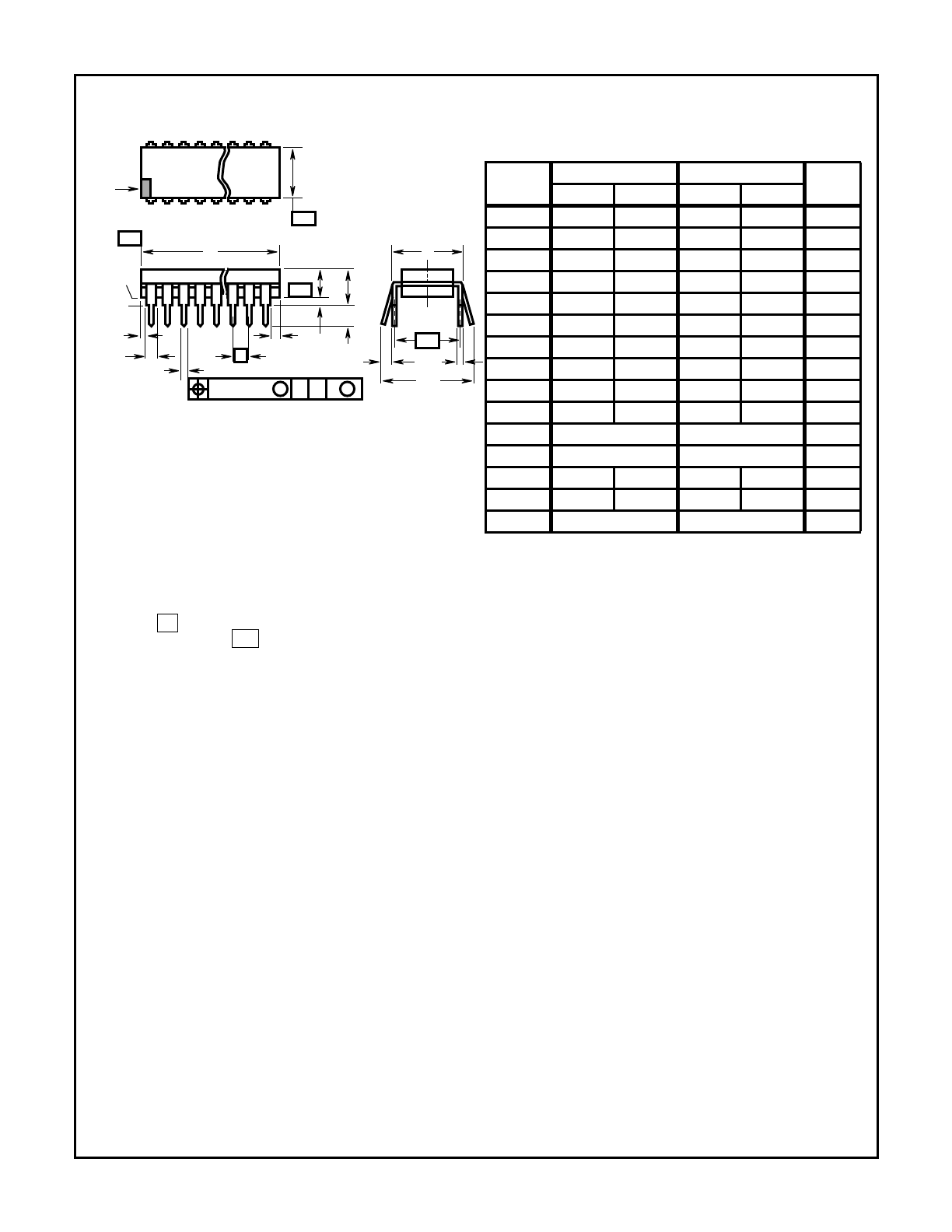
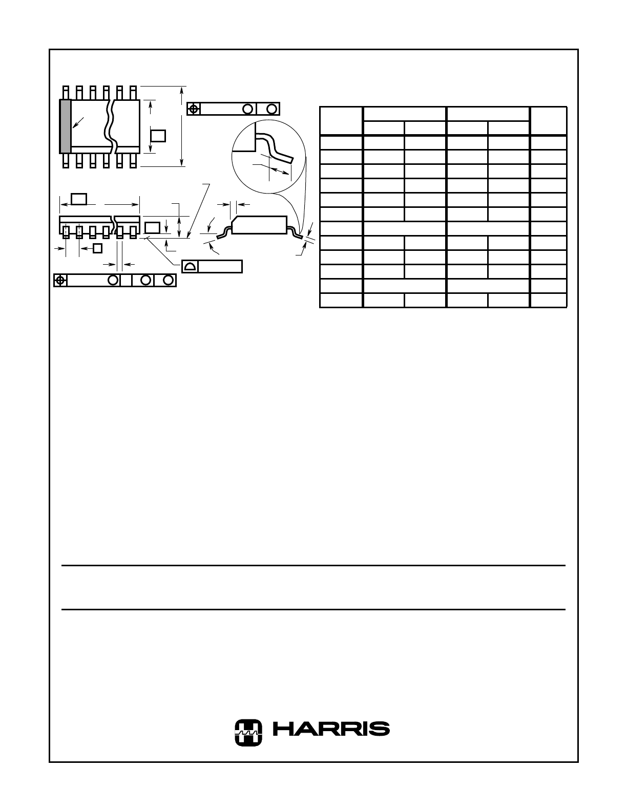
Dual-In-Line Plastic Packages (PDIP)
E8.3
(JEDEC MS-001-BA ISSUE D)
8 LEAD DUAL-IN-LINE PLASTIC PACKAGE
SYMBOL
INCHES
MILLIMETERS
NOTES
MIN
MAX
MIN
MAX
A
-
0.210
-
5.33
4
A1
0.015
-
0.39
-
4
A2
0.115
0.195
2.93
4.95
-
B
0.014
0.022
0.356
0.558
-
B1
0.045
0.070
1.15
1.77
8, 10
C
0.008
0.014
0.204
0.355
-
D
0.355
0.400
9.01
10.16
5
D1
0.005
-
0.13
-
5
E
0.300
0.325
7.62
8.25
6
E1
0.240
0.280
6.10
7.11
5
e
0.100 BSC
2.54 BSC
-
e
A
0.300 BSC
7.62 BSC
6
e
B
-
0.430
-
10.92
7
L
0.115
0.150
2.93
3.81
4
N
8
8
9
Rev. 0 12/93
11
All Harris Semiconductor products are manufactured, assembled and tested under ISO9000 quality systems certification.
Harris Semiconductor products are sold by description only. Harris Semiconductor reserves the right to make changes in circuit design and/or specifications at
any time without notice. Accordingly, the reader is cautioned to verify that data sheets are current before placing orders. Information furnished by Harris is
believed to be accurate and reliable. However, no responsibility is assumed by Harris or its subsidiaries for its use; nor for any infringements of patents or other
rights of third parties which may result from its use. No license is granted by implication or otherwise under any patent or patent rights of Harris or its subsidiaries.
Sales Office Headquarters
For general information regarding Harris Semiconductor and its products, call 1-800-4-HARRIS
NORTH AMERICA
Harris Semiconductor
P. O. Box 883, Mail Stop 53-210
Melbourne, FL 32902
TEL: 1-800-442-7747
(407) 729-4984
FAX: (407) 729-5321
EUROPE
Harris Semiconductor
Mercure Center
100, Rue de la Fusee
1130 Brussels, Belgium
TEL: (32) 2.724.2111
FAX: (32) 2.724.22.05
ASIA
Harris Semiconductor PTE Ltd.
No. 1 Tannery Road
Cencon 1, #09-01
Singapore 1334
TEL: (65) 748-4200
FAX: (65) 748-0400
S E M I C O N D U C T O R
HIP7020
NOTES:
1. Symbols are defined in the “MO Series Symbol List” in Section
2.2 of Publication Number 95.
2. Dimensioning and tolerancing per ANSI Y14.5M-1982.
3. Dimension “D” does not include mold flash, protrusions or gate
burrs. Mold flash, protrusion and gate burrs shall not exceed
0.15mm (0.006 inch) per side.
4. Dimension “E” does not include interlead flash or protrusions. In-
terlead flash and protrusions shall not exceed 0.25mm (0.010
inch) per side.
5. The chamfer on the body is optional. If it is not present, a visual
index feature must be located within the crosshatched area.
6. “L” is the length of terminal for soldering to a substrate.
7. “N” is the number of terminal positions.
8. Terminal numbers are shown for reference only.
9. The lead width “B”, as measured 0.36mm (0.014 inch) or greater
above the seating plane, shall not exceed a maximum value of
0.61mm (0.024 inch).
10. Controlling dimension: MILLIMETER. Converted inch dimen-
sions are not necessarily exact.
INDEX
AREA
E
D
N
1
2
3
-B-
0.25(0.010)
C A
M
B S
e
-A-
L
B
M
-C-
A1
A
SEATING PLANE
0.10(0.004)
h x 45
o
C
H
0.25(0.010)
B
M
M
α
Small Outline Plastic Packages (SOIC)
M8.15
(JEDEC MS-012-AA ISSUE C)
8 LEAD NARROW BODY SMALL OUTLINE PLASTIC PACKAGE
SYMBOL
INCHES
MILLIMETERS
NOTES
MIN
MAX
MIN
MAX
A
0.0532
0.0688
1.35
1.75
-
A1
0.0040
0.0098
0.10
0.25
-
B
0.013
0.020
0.33
0.51
9
C
0.0075
0.0098
0.19
0.25
-
D
0.1890
0.1968
4.80
5.00
3
E
0.1497
0.1574
3.80
4.00
4
e
0.050 BSC
1.27 BSC
-
H
0.2284
0.2440
5.80
6.20
-
h
0.0099
0.0196
0.25
0.50
5
L
0.016
0.050
0.40
1.27
6
N
8
8
7
α
0
o
8
o
0
o
8
o
-
Rev. 0 12/93