
CAUTION: These devices are sensitive to electrostatic discharge. Users should follow proper I.C. Handling Procedures.
Copyright
©
Harris Corporation 1994
1
S E M I C O N D U C T O R
Description
The Harris HIP7010, J1850 Byte Level Interface Circuit, is a
member of the Harris family of low-cost multiplexed wiring
ICs. The integrated functions of the HIP7010 provide the
system designer with components key to building a “Class
B” multiplexed communications network interface, which
fully conforms to the VPW Multiplexed Wiring protocol
specified in the SAE J1850 Standard. The HIP7010 is
designed to interface with a wide variety of Host
microcontrollers via a standard three wire, high-speed
(1MHz), synchronous, serial interface. The HIP7010
automatically produces properly framed VPW messages,
appending the Start of Frame (SOF) symbol and calculating
and appending the CRC check byte. All circuitry needed to
decode incoming messages, to validate CRC bytes, and to
detect Breaks, End of Data (EOD), Idle bus, and illegal
symbols is included. In-Frame Responses (IFRs) are fully
supported for Type 1, Type 2, and Type 3 messages, with
the appropriate Normalization Bit automatically generated.
The HCMOS design allows proper operation at various input
frequencies from 2MHz to 12MHz. Connection to the J1850
Bus is via a Harris HIP7020.
Ordering Information
PART
NUMBER
TEMPERATURE
RANGE
PACKAGE
HIP7010P
-40
o
C +125
o
C
14 Lead Plastic DIP
HIP7010B
-40
o
C +125
o
C
14 Lead Plastic SOIC (N)
HIP7010
J1850 Byte Level Interface Circuit
Features
• Fully Supports VPW (Variable Pulse Width) Messaging
Practices of SAE J1850 Standard for Class B Data
Communications Network Interface
- 3-Wire, High-Speed, Synchronous, Serial Interface
• Reduces Wiring Overhead
• Directly Interfaces with 68HC05 and 68HC11 Style SPI
Ports
• 1MHz, 8-Bit Transfers Between Host and HIP7010 Min-
imize Host Service Requirements
• Automatically Transmits Properly Framed Messages
• Prepends SOF to First Byte and Appends CRC to Last
Byte
• Fail-Safe Design Including, Slow Clock Detection
Circuitry, Prevents J1850 Bus Lockup Due to System
Errors or Loss of Input Clock
• Automatic Collision Detection
• End of Data (EOD), Break, Idle Bus, and Invalid Symbol
(Noise/Illegal Symbols) Detection
• Supports In-Frame Responses with Generation of
Normalization Bits (NB) for Type 1, Type 2, and Type 3
Messages
• Wait-For-Next-Idle Mode Reduces Host Overhead During
Non-Applicable Messages
• Status Register Flags Provide Information on Current
Status of J1850 Bus
• Serial I/O Pins are Active Only During Transfers - Bus
Available for Other Devices 95% of the Time
• High Speed (4X) Receive Mode for Production and
Diagnostic Testing/Programming
• TEST Pin Provides Built-in-Test Capabilities for In-
System Diagnostics and Factory Testing
• Operates with Wide Range of Input Clock Frequencies
• Power-Saving Power-Down Mode
• Full -40
o
C to +125
o
C Operating Range
• Single 3.0V to 6.0V Supply
File Number
3644.1
ADVANCE INFORMATION
November 1994
Pinout
HIP7010 (SOIC, PDIP)
TOP VIEW
IDLE
VPWIN
VPWOUT
V
DD
RESET
TEST
SACTIVE
RDY
STAT
CLK
V
SS
SIN
SOUT
SCK
1
2
3
4
5
6
7
14
13
12
11
10
9
8
2
HIP7010
Block Diagram
Pin Description
PIN NUMBER
PIN NAME
IN/OUT
PIN DESCRIPTION
1
IDLE
OUT
CMOS Output
2
VPWIN
IN
CMOS Schmitt (No V
DD
Diode)
3
VPWOUT
OUT
CMOS Output
4
V
DD
-
Power Supply
5
RESET
IN
CMOS Schmitt (No V
DD
Diode)
6
TEST
IN
CMOS Input with Pull-Down
7
SACTIVE
OUT
CMOS Output
8
SCK
OUT
Three-State with Pull-Down
9
SOUT
OUT
Three-State with Pull-Down
10
SIN
IN
CMOS Input with Pull-Down
11
V
SS
-
Ground
12
CLK
IN
CMOS Schmitt (No V
DD
Diode)
13
STAT
IN
CMOS Input with Pull-Down
14
RDY
IN
CMOS Input with Pull-Down
10
9
SOUT
SIN
7
6
5
12
TEST
V
SS
11
CLK
13
14
1
8
STAT
RDY
SCK
2
3
VPWOUT
GENERATOR
TIMING
STATE MACHINE
AND CONTROL LOGIC
DECODED VPW IN
OUTPUT DATA
J1850 VPW SYMBOL
ENCODER/DECODER
LSB
MSB
STATUS/CONTROL BYTE
V
DD
4
A
B
C
MUX
CRC GENERATOR/CHECKER
A
C
MUX
DATA SHIFT REGISTER
IDLE
RESET
SACTIVE
VPWIN
3
Specifications HIP7010
Absolute Maximum Ratings
Thermal Information
Supply Voltage (V
DD
) . . . . . . . . . . . . . . . . . . . . . . . . .-0.3V to +7.0V
Input or Output Voltage
Pins with V
DD
Diode . . . . . . . . . . . . . . . . . . . . -0.3V to V
DD
+0.3V
Pins without V
DD
Diode. . . . . . . . . . . . . . . . . . . . .-0.3V to +10.0V
ESD Classification . . . . . . . . . . . . . . . . . . . . . . . . . . . . . . . . Class 2
Gate Count . . . . . . . . . . . . . . . . . . . . . . . . . . . . . . . . . . +2500 Gates
Thermal Resistance
θ
JA
Plastic DIP Package . . . . . . . . . . . . . . . . . . . . . . . . . .+100
o
C/W
SOIC Package. . . . . . . . . . . . . . . . . . . . . . . . . . . . . . .+120
o
C/W
Maximum Package Power Dissipation at +125
o
C
DIP Package . . . . . . . . . . . . . . . . . . . . . . . . . . . . . . . . . . . 250mW
SOIC Package. . . . . . . . . . . . . . . . . . . . . . . . . . . . . . . . . . 200mW
Operating Temperature Range (T
A
) . . . . . . . . . . . .-40
o
C to +125
o
C
Storage Temperature Range (T
STG
) . . . . . . . . . . . .-65
o
C to +150
o
C
Junction Temperature . . . . . . . . . . . . . . . . . . . . . . . . . . . . . . +150
o
C
Lead Temperature (Soldering, 10s). . . . . . . . . . . . . . . . . . . . +265
o
C
CAUTION: Stresses above those listed in “Absolute Maximum Ratings” may cause permanent damage to the device. This is a stress only rating and operation
of the device at these or any other conditions above those indicated in the operational sections of this specification is not implied.
Operating Conditions
Operating Voltage Range . . . . . . . . . . . . . . . . . . . . . +3.0V to +5.5V
Operating Temperature Range . . . . . . . . . . . . . . . . -40
o
C to +125
o
C
Input Low Voltage . . . . . . . . . . . . . . . . . . . . . . . . . . . . . . 0V to +0.8V
Input High Voltage. . . . . . . . . . . . . . . . . . . . . . . . . . .(0.8V
DD
) to V
DD
Input Rise and Fall Time
CMOS Inputs . . . . . . . . . . . . . . . . . . . . . . . . . . . . . . . . 100ns Max
CMOS Schmitt Inputs . . . . . . . . . . . . . . . . . . . . . . . . . . .Unlimited
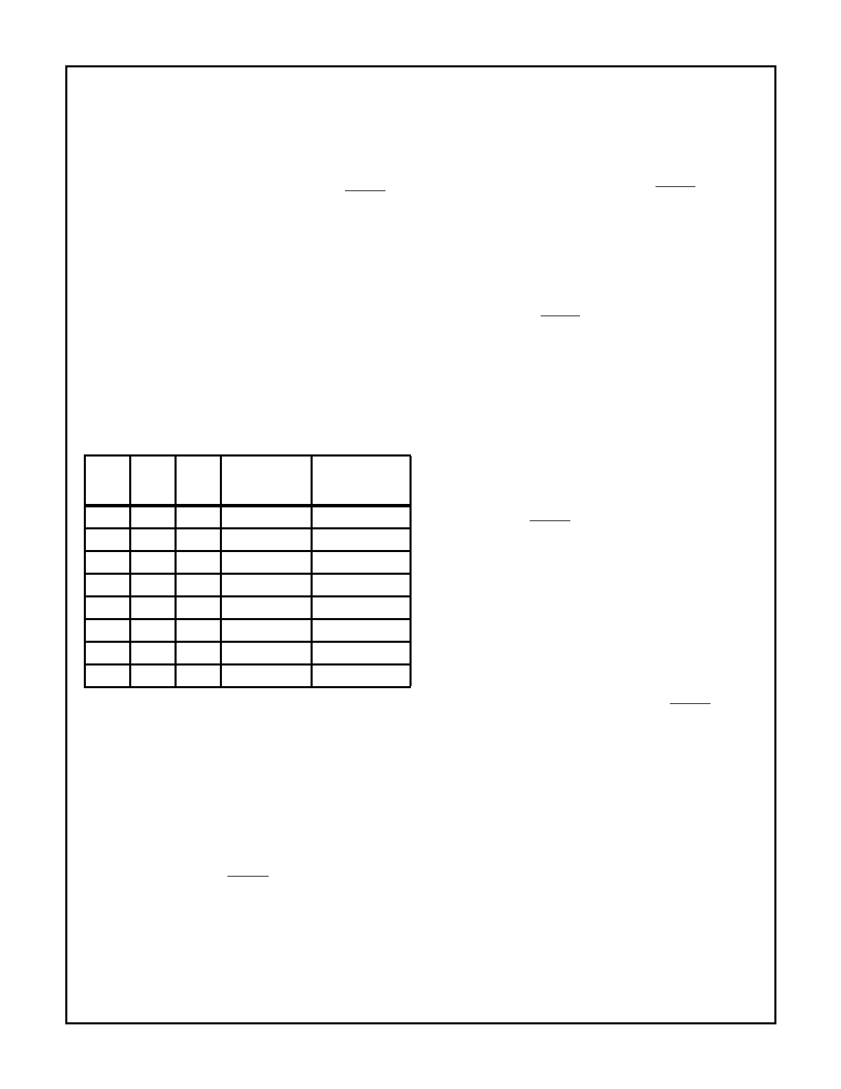
Electrical Specifications
T
A
= -40
o
C to +125
o
C, V
DD
= 5V
DC
±
10%, Unless Otherwise Specified
PARAMETERS
SYMBOL
CONDITIONS
MIN
TYP
MAX
UNITS
Supply Current
Operating Current
I
OP
CLK = 2.0 MHz
-
1.0
-
mA
Power-Down Mode (Note 1)
I
PD
PD = 1
-
5.0
-
µ
A
Clock Stopped (Note 2)
I
STOP
CLK = V
SS
or V
DD
-
5.0
-
µ
A
Input High Voltage
CMOS Level (SIN, STAT, RDY, TEST)
V
IH
0.7V
DD
-
V
DD
V
Schmitt Trigger (RESET, CLK, VPWIN)
0.8V
DD
-
V
DD
V
Input Low Voltage
CMOS Level (SIN, STAT, RDY, TEST)
V
IL
V
SS
-
0.3V
DD
V
Schmitt Trigger (RESET, CLK, VPWIN)
V
SS
-
0.2V
DD
V
High Level Input Current
(CLK, VPWIN, RESET)
I
IH
V
IN
= V
DD
-1
0.001
1
µ
A
Input Buffer with Pull-down (SIN, TEST, STAT, RDY)
100
TBD
500
µ
A
Low Level Input Current
(SIN, CLK, STAT, RDY, VPWIN, RESET, TEST)
I
IL
V
IN
= V
SS
-1
-0.001
1
µ
A
Output High Voltage
(SCK, SOUT, VPWOUT, IDLE, SACTIVE)
V
OH
I
LOAD
= 0.8 mA
V
DD
-0.8
-
-
V
Output Low Voltage
(SCK, SOUT, VPWOUT, IDLE, SACTIVE)
V
OL
I
LOAD
= -1.6 mA
-
-
0.4
V
High Impedance Leakage Current
Three-State with Pull-down (SCK, SOUT)
I
OZ
V
OUT
= V
DD
100
-0.01
500
µ
A
V
OUT
= V
SS
-10
10
µ
A
Schmitt Trigger Hysteresis Voltage
(RESET, CLK, VPWIN)
V
HYS
0.2
0.5
2.0
V
NOTES:
1. SIN, STAT, RDY, and TEST = V
SS
; VPWIN = V
DD
; CLK = 10MHz
2. SIN, STAT, RDY, and TEST = V
SS
; SACTIVE and VPWIN = V
DD
4
Specifications HIP7010
Serial Interface Timing
(See Figure 1- Figure 7) T
A
= -40
o
C to +125
o
C, V
DD
= 5V
DC
±
10%, Unless Otherwise Specified
NUMBER
SYMBOL
PARAMETERS
MIN
TYP
MAX
UNITS
-
-
Operating Frequency
2
8
12
MHz
(1)
t
CYC
SCK Cycle Time
-
1.0
-
MHz
(2)
t
LEAD
SACTIVE Lead Time
Before Status/Control Transfer
450
718
850
ns
Before Data Transfer
1200
1250
1350
ns
(3)
t
LAG
SACTIVE Lag Time
After Status/Control Transfer
650
750
850
ns
After Data Transfer
1200
1250
1350
ns
(4)
t
SCKH
Clock (SCK) HIGH Time
450
500
550
ns
(5)
t
SCKL
Clock (SCK) LOW Time
450
500
550
ns
(6)
t
DVSCK
Required Data In Setup Time (SIN to SCK)
-
10
40
ns
(7)
t
SCKDX
Required Data In Hold Time (SIN after SCK)
-
10
40
ns
(8)
t
DZDA
Data Active from High Impedance Delay (SACTIVE to SOUT Active)
0
10
-
ns
(9)
t
DADZ
Data Active to High Impedance Delay (SACTIVE to SOUT High
Impedance)
-
10
40
ns
(10)
t
SCKDV
Data Out Setup Time (SCK to SOUT)
375
475
-
ns
(11)
t
DXSCK
Data Out Hold Time (SOUT after SCK)
375
475
-
ns
(12)
t
RISE
Output Rise Time (0.3V
DD
to 0.7V
DD
, C
L
= 100pF)
20
50
75
ns
(13)
t
FALL
Output Fall Time (0.7V
DD
to 0.3V
DD
, C
L
= 100pF)
20
50
75
ns
(14)
t
STATH
Required STAT Pulse Width
-
20
75
ns
(15)
t
RDYH
Required RDY Pulse Width
-
20
75
ns
t
RESETL
Required RESET Pulse Width
-
20
75
ns
(16)
t
SACTIVE
SACTIVE Delay from RDY (IDLE = V
SS
)
1150
1750
2350
ns
SACTIVE Delay from STAT (FTU = 0)
5
285
850
ns
(17)
t
RDYSCK
Required RDY Removal Time Prior to Last SCK for Short RDY
-
25
100
ns
(18)
t
SCKRDY
Required RDY Hold Time after Last SCK for Long RDY
-
0
50
ns
(19)
t
REC
Required SERIAL Recovery Time (Minimum Time after SACTIVE
Until Next RDY/STAT)
-
0
100
ns

5
HIP7010
FIGURE 1. SERIAL INTERFACE TIMING DIAGRAM
NOTES:
1. Measurement points are from V
DD
/2, except 12 and 13 which are measured between V
IL
and V
IH.
2. All timings assume proper CLK frequency and Divide Select values to generate 1MHz SCK.
(OUTPUT)
SCK
(OUTPUT)
SIN
(INPUT)
SOUT
(OUTPUT)
D7I
D6I
D0I
D7O
D6O
D0O
(6)
(11)
(8)
(5)
(12)
(13)
(1)
(4)
(7)
SACTIVE
(INPUT)
RDY (LONG)
(INPUT)
RDY (SHORT)
STAT
(INPUT)
(2)
(10)
(9)
(3)
(14)
(15)
(16)
(17)
(18)
(19)
Functional Pin Description
This section provides a description of each of the 14 pins of
the HIP7010 as shown in Figure 2.
FIGURE 2. 14 PIN DIP AND SO TERMINAL ASSIGNMENTS
V
DD
and V
SS
(Power)
Power is supplied to the HIP7010 using these two pins. V
DD
is connected to the positive supply and V
SS
is connected to
the negative supply.
IDLE
VPWIN
VPWOUT
V
DD
RESET
TEST
SACTIVE
RDY
STAT
CLK
V
SS
SIN
SOUT
SCK
1
2
3
4
5
6
7
14
13
12
11
10
9
8
CLK (Clock - Input)
The Clock input (CLK) provides the basic time base reference for
all J1850 symbol detection and generation. Serial Bus transfers
between the HIP7010 and the Host microcontroller are also
timed based on the Clock input. Proper VPW symbol detection
and generation requires a 2MHz clock which is internally derived
from the CLK input. Various CLK input frequencies can be
accommodated via the Divide Select bits in the Status/Control
Register (see Status/Control Register for details).
An internal Slow Clock Detect circuit monitors the CLK input
signal and generates a HIP7010 reset if the clock is inactive
for more than 2
µ
s. This is a safety mechanism to prevent
blocking the J1850 and Serial busses in the event of a clock
failure. The Slow Clock Detect reset can also be intentionally
invoked by externally inhibiting CLK input transitions.
Power can be reduced under Host control via the Power-
Down bit in the Status/Control Register (see Status/Control
Register for details). Setting the Power-Down bit effectively
stops internal clocking of the HIP7010.

6
HIP7010
For enhanced noise immunity, the CLK input is a CMOS Schmitt
trigger input. See Electrical Specifications for input levels.
VPWOUT (Variable Pulse Width Out - Output),
VPWIN (Variable Pulse Width In - Input)
These two lines are used to interface to a J1850 bus trans-
ceiver, such as the Harris HIP7020. VPWOUT is the variable
pulse width modulated output of the HIP7010’s symbol
encoder circuit. VPWIN is the inverted input to the symbol
decoder of the HIP7010. VPWIN is a schmitt input.
SIN (Serial In - Input),
SOUT (Serial Out - Output),
SCK (Serial Clock - Output),
SACTIVE (Serial Bus Active - Output)
These four lines constitute the synchronous Serial Interface
(SERIAL) interface of the HIP7010. See the Serial Interface
(SERIAL) System for details. SIN, SOUT, and SCK provide
the three principal connections to the Host controller. SIN is a
CMOS input. SOUT and SCK are three-state outputs which
are only activated during serial transfers. The SIN, SOUT, and
SCK pins contain integrated pull-down load devices which
provide termination on the bus whenever it is in a high imped-
ance state. The SACTIVE pin is a CMOS output, which pulls
low when the HIP7010 is communicating on the serial bus.
See Serial Interface (SERIAL) System and Applications
Information for more details.
RDY (Byte Ready - Input)
The Byte Ready (RDY) line is a “handshaking” input from the
Host. Each rising edge on the RDY pin signifies that the Host has
loaded a byte into its SERIAL transmit register and the HIP7010
can retrieve it (by generating clocks on SCK) when the HIP7010
is ready for the data. See Serial Interface (SERIAL) System
and Applications Information for more details.
The RDY pin contains an integrated pull-down load device
which will hold the pin low if it is left unconnected.
IDLE (Idle/Service Request - Output)
The IDLE output pin indicates that the J1850 Bus has been
in a passive state for at least 300
µ
s and is now idle. If the
bus has been passive for a minimum of 239
µ
s and another
node initiates a new message, IDLE will pulse low for 1
µ
s.
In its role as a Service Request pin, a reset forces IDLE
high. Following the reset, IDLE remains high for 17 CLK
cycles and is then driven low. IDLE will remain low until 40
CLK cycles +1.5
µ
s after completion of the first Status/Con-
trol byte transfer. The IDLE pin will then resume its normal
role, remaining high until a 300
µ
s lull (or 239
µ
s plus a pas-
sive to active transition) has been detected on the J1850
bus. This provides a handshake mechanism to ensure the
Host will reinitialize the HIP7010 each time the HIP7010 is
reset via POR, RESET, or Slow Clock Detect.
If IDLE is low when an echo failure causes the ERR bit to be
set in the Status byte, the IDLE pin will pulse high for 2
µ
s
and then return low (see Status/Control Register).
If IDLE is low when the host sets the NXT bit in the control
byte, the IDLE pin will pulse high for 2
µ
s and then return low
(see Status/Control Register).
In general a Status/Control byte transfer should be performed
each time IDLE goes low. See Effects of Resets and Power-
Down and Applications Information for more details.
The IDLE pin is an active low CMOS output. See Operation
of the HIP7010 for more details.
STAT (Request Status/Control - Input)
The Request Status/Control (STAT) input pin is used by the
Host microcontroller to initiate an exchange of the Host’s con-
trol byte and the HIP7010’s status byte. A low to high transi-
tion on the STAT input signals the HIP7010 that the Host has
placed a control word in it’s SERIAL output register and is
ready to exchange it with the HIP7010’s status word. The
HIP7010 controls the exchange by generating the 8 SCKs
required. See Serial Interface (SERIAL) System and Appli-
cations Information for more details.
The STAT pin contains an integrated pull-down load device
which will hold the pin low if it is left unconnected.
RESET (Reset - Input)
The RESET input is a low level active input, which resets the
HIP7010. Resetting the HIP7010 forces SACTIVE high, dis-
ables the SOUT and SCK pins, forces the VPWOUT output
low, drives IDLE high, and returns the internal state machine
to its initial state. Following reset, the HIP7010 is inhibited
from transmitting or receiving J1850 messages until a Sta-
tus/Control Register transfer has been completed (see
Effects Of Resets And Power-Down for more details).
The HIP7010 is also reset during initial power-on, by an
internal power-on-reset (POR) circuit.
Loss of a clock on the CLK input will cause a reset as
described previously under CLK.
If not used, the RESET pin should be tied to V
DD
.
For enhanced noise immunity, the CLK input is a CMOS Schmitt
trigger input. See Electrical Specifications for input levels.
TEST (Test Mode - Input)
The TEST input provides a convenient method to test the
HIP7010 at the component level. Raising the TEST pin to a
high level causes the HIP7010 to enter a special TEST mode.
In the TEST mode, a special portion of the state machine is
activated which provides access to the Built-in-Test and diag-
nostic capabilities of the HIP7010 (see Test Mode for more
details).
The TEST pin contains an integrated pull-down load device
which will hold the pin low if it is left unconnected. In many
applications the TEST pin will be left unconnected, to allow
access via a board level ATE tester.
J1850 VPW Messaging
This section provides an introduction to J1850 multiplexed
communications. It is assumed that the user is or will
become familiar with the appropriate documents published
by the Society of Automotive Engineering (SAE). The follow-
ing discussion is not comprehensive.

7
HIP7010
Overview
The SAE J1850 Standard (Note 1) (J1850) establishes the
requirements for communications on a Class B multiplexed
wiring network for automotive applications. The J1850 docu-
ment details the requirements in a three layer description
which separately specifies the characteristics of the
physical
layer, the data link layer, and the application layer. There are
several options within each layer which allows vehicle manu-
facturers to customize the network while still maintaining a
level of universality.
NOTE:
1. SAE J1850 Standard, Class B Data Communication Network
Interface, May 1994, Society of Automotive Engineers Inc.
The hardware of the Harris HIP7010 provides features which
facilitate implementation of the 10.4Kbps Variable Pulse
Width Modulated (VPW) physical layer option of J1850. In
combination with a bus transceiver, such as the Harris J1850
Bus Transceiver HIP7020, and appropriate software algo-
rithms the HIP7010 circuitry enables the designer to com-
pletely implement a 10.4Kbps VPW Class B
Communications Network Interface per J1850. Features of
such an implementation include:
• Single Wire 10.4Kbps Communications
• Bit-by-Bit Bus Arbitration
• Industry Standard Protocol
• Message Acknowledgment (“In-Frame Response”) Capa-
bilities
• Exceptionally Tolerant of Clock Skew, System Noise, and
Ground Offsets
• Meets CARB and EPA Diagnostic Requirements
• Supports up to 32 Nodes
• Low Error Rates
• Excellent EMC Levels (when interfaced via Harris J1850
Bus Transceiver HIP7020)
In addition to the standard J1850 features, the HIP7010 hard-
ware provides a high speed mode, (intended for receive only
use) which can significantly enhance vehicle maintenance
capabilities. The high speed mode provides a 41.6Kbps com-
munications path to any node built with the HIP7010.
Anatomy of a J1850 VPW Message
All messages in a J1850 VPW system are sent along a single
wire, shared bus. At any given moment the bus can be in
either of two states:
active (high) or passive (low). Multiple
nodes are connected to the bus as a “wired-OR” network in
which the bus is high if
any one (or more) node is generating
an active output. The bus is only low when
no nodes are gen-
erating active outputs. It follows that, when no communica-
tions are taking place the bus will rest in the passive state. A
message begins when the bus is first driven to the high state.
Each succeeding state transition (i.e. - a change from active to
passive or passive to active) transfers one bit of information
(
symbol) until the message is complete and the bus once
again rests at the passive state. The interpretation of each
symbol in the message is dependent on its duration (and
state), hence the descriptor Variable Pulse Width (VPW).
Each message has a beginning and an end, the span of
which encompasses the entire
message or frame (refer to
Figure 3). A frame consists of an active
start of frame (SOF)
symbol and a passive
end of frame (EOF) symbol sandwiched
around a series of byte sized (8-bit) groups of symbols. The
first byte of the frame contents is always a
header byte, fol-
lowed by possibly additional header bytes, followed by one or
more
data bytes, followed by an integrity check byte (CRC
byte), followed by a passive
end of data (EOD) symbol, fol-
lowed by possibly one or more
in-frame-response (IFR) bytes.
To keep waiting times low, messages are limited to 12 bytes
total (including header, data, check, and IFR bytes). All mes-
sage bytes are transmitted most significant bit (MSB) first.
VPW Symbol Definitions
Within the J1850 scheme, symbols are defined in terms of both
duration and state (passive or active). The duration is mea-
sured as the time between successive transitions. There is one
transition per symbol and one symbol per transition. The end of
one symbol marks the beginning of the next. Since the bus is
passive when a message begins and must return to that same
state when the message completes, all frames have an even
number of transitions and hence an even number of symbols.
There are unique definitions for data bit symbols (all the sym-
bols which occur within the header, data, and check bytes) and
protocol symbols (including SOF, EOD, and EOF). The duration
of each symbol is expressed in terms of VPW Timing Pulses
(TV values). Table 1 summarizes the TV definitions. Each TV is
specified in terms of a
nominal (or ideal) duration and a mini-
mum and maximum duration. The span between the minimum
and maximum limits accommodates system noise sources
such as node to node clock skew, ground offsets, clock jitter,
and electromechanical noise. There are no dead zones
between the maximum of one TV and the minimum of the next.
FIGURE 3. TYPICAL J1850 VPW MESSAGE FRAME
SOF
HEADER
DATA 1
DATA 2
CRC
EOD
EOF
8
HIP7010
The terms
short and long are often used to refer to pulses of
duration TV1 and TV2 respectively.
VPW is a non-return-to-zero (NRZ) protocol in which each
transition represents a complete bit of information. Accord-
ingly, a
0 data bit will sometimes be transmitted as a passive
pulse and sometimes as an active pulse. Similarly, a
1 data
bit will sometimes be transmitted as a passive pulse and
sometimes as an active pulse. In order to accommodate
arbitration (see Bus Arbitration) a
long active pulse repre-
sents a 0 data bit and a
short active pulse represents a 1
data bit. Complementing this fact, a
short passive pulse rep-
resents a 0 and a
long passive pulse represents a 1. Starting
from a transition to the active state, a 0 data bit will maintain
the active level longer than a 1. Similarly, starting from a
transition to the passive state, a 0 data bit will return to the
active level quicker than a 1. These facts give rise to the
dominance of 0’s over 1’s on the J1850 bus as depicted in
Figure 4. See Bus Arbitration for additional details.
FIGURE 4A. DOMINANCE OF ACTIVE 0 DATA BIT
FIGURE 4B. DOMINANCE OF PASSIVE 0 DATA BIT
FIGURE 4.
TABLE 1. J1850 TV DEFINITIONS
TV ID
DURATION (ALL TIMES IN
µ
s)
MINIMUM
NOMINAL
MAXIMUM
Illegal
0
NA
≤
34
TV1
>34
64
≤
96
TV2
>96
128
≤
163
TV3
>163
200
≤
239
TV4
>239
280
NA
TV5
>239
300
NA
TV6
>280
300
NA
BIT
DATA
0
BIT
DATA
1
BUS
J1850
SYNCHRONIZED
PULSE (0)
LONGER ACTIVE
0
0
1
CONTROLS THE BUS
BIT
DATA
0
BIT
DATA
1
BUS
J1850
SYNCHRONIZED
PULSE (0)
SHORTER PASSIVE
0
0
1
CONTROLS THE BUS
Table 2 summarizes the complete set of symbol definitions
based on duration and state.
In Frame Response (IFR)
The distinction between two of the passive symbols, EOD and
EOF, is subtle but important (refer to Figure 5). The EOD (TV3)
interval signifies that the originator of the message is done
broadcasting and any nodes which have been requested to
respond (i.e. - to acknowledge receipt of the message) can now
do so. The EOD interval begins when the transmitting node has
completed sending the eighth bit of the check byte. The trans-
mitter simply releases the bus and allows it to revert to a pas-
sive state. In the course of normal messaging, no node can
seize the bus until an EOD time has been detected. Once an
EOD has elapsed, any nodes which are scheduled to produce
an IFR will arbitrate for control of the bus (see Bus Arbitration)
and respond appropriately. If no responses are forthcoming the
bus remains in the passive state until an EOF (TV4) interval
has elapsed. After the EOF has been generated, the frame is
considered closed and the next communications on the bus will
represent a totally new message.
IFRs can consist of multiple bytes from a single respondent,
one byte from a single respondent, or one byte from multiple
respondents. In all cases the first response byte must be pre-
ceded by a
normalization bit (NB) which serves as a start of
response symbol and places the bus in an active state so that
following the IFR byte(s) the bus will be left in the passive state.
The NB symbol is by definition active, but can be either TV1
or TV2 in duration. The long variety (TV2) signifies the IFR
contains a CRC byte. The short variety (TV1) precedes an
IFR without CRC.
Message Types
Messages are classified into one of four
Types according to
whether the message has an IFR and what kind of IFR it is.
The definitions are:
• Type 0 - No IFR
• Type 1 - One byte IFR from a single respondent
(no CRC byte)
• Type 2 - One byte IFRs from multiple respondents
(no CRC byte)
• Type 3 - Multiple byte IFR from a single respondent
(CRC appended)
TABLE 2. J1850 SYMBOL DEFINITIONS
SYMBOL
DEFINITION
0 Data
Passive TV1 or Active TV2
1 Data
Active TV1 or Passive TV2
SOF (Start of Frame)
Active TV3
EOD (End of Data)
Passive TV3
EOF (End of Frame)
Passive TV4
IFS (Inter-Frame Separation)
Passive TV6
IDLE (Idle Bus)
Passive >TV6 Nominal
NB (Normalization Bit)
ActiveTV1 or Active TV2
BRK (Break)
Active TV5
9
HIP7010
Bus Arbitration
The nature of multiplexed communications leads to contention
issues when two or more nodes attempt to transmit on the bus
simultaneously. Within J1850 VPW systems, messages are
assigned varying levels of priority which allows implementa-
tion of an arbitration scheme to resolve potential contentions.
The specified arbitration is performed on a symbol by symbol
basis throughout the duration of every message.
Arbitration begins with the rising edge of the SOF pulse. No
node should attempt to issue an SOF until an Idle bus has
been detected (i.e. - an
Inter-Frame Separation (IFS) symbol
with a period of TV6 has been received). If multiple nodes are
ready to access the bus and are all waiting for an IFS to
elapse, invariable skews in timing components will cause one
arbitrary node to detect the Idle condition before all others and
start transmission first. For this reason, all nodes waiting for
an IFS will consider an IFS to have occurred if either:
1. An IFS nominal period has elapsed
or
2. An EOF minimum period has elapsed
and a rising edge
has been detected
Arbitrating devices will all be synchronized during the SOF.
Beginning with the first data bit and continuing to the EOF,
every transmitting device is responsible for verifying that the
symbol it sent was the symbol which appeared on the bus.
Each transition, every transmitting node must decode the
symbol, verify the received symbol matches the one sent, and
begin timing of the next symbol. Since timing of the next sym-
bol begins with the last transition detected on the bus, all
transmitters are re-synchronized each symbol. When the
received symbol doesn’t match the symbol sent, a conflict (
bit
collision) occurs. Any device detecting a collision will assume
it has lost arbitration and immediately relinquish the bus. Typi-
cally, after losing arbitration, a device will attempt retransmis-
sion of the message when the bus once again becomes idle.
The definition of 1 and 0 data bits (see Table 2 and discussion
under VPW Symbol Definitions) leads to 0’s having priority
over 1’s in this arbitration scheme. Header bytes are generally
assigned such that arbitration is completed before the first
data byte is transmitted. Because of the dominance of 0 bits
and the MSB first bit order, a header with the hexadecimal
value $00 will have highest priority, then $01, $02, $03, etc.
An example of two nodes arbitrating for control of the bus is
shown in Figure 6.
Arbitration also takes place during the IFR portion of a mes-
sage, if more than one node is attempting to generate a
response. Arbitration begins with the NB symbol, which fol-
lows the EOD and precedes the first IFR byte.
For Type 1 and Type 3 messages only, the respondent which
successfully arbitrates for control of the bus produces an IFR.
All other respondents abort their IFRs.
For Type 2 messages, all respondents which lose arbitration
must count symbols and re-attempt transmission at the end of
each byte. Each node, which successfully responds, elimi-
nates itself from the subsequent arbitration until all nodes
have responded. This arbitration scheme limits each respon-
dent to a single byte during a Type 2 IFR.
Break
To force a message to be aborted before EOF is reached, a
break (BRK) symbol can be transmitted by any node. The
BRK symbol is an active pulse of duration TV5. Reception of a
break causes all nodes to reset to a
ready-to-receive state
and to re-arbitrate for control following an IFS.
HIP7010 Architectural Overview
The HIP7010 consists of three major functional blocks: the
Serial Interface System (SERIAL) block; the State Machine
(STATE) block; and the Symbol Encoder/Decoder (SENDEC)
block. Transfers between the Host and the HIP7010 are con-
trolled by the SERIAL block, while transfers between the
J1850 bus and the HIP7010 are handled by the SENDEC
FIGURE 5. J1850 MESSAGE WITH IN-FRAME-RESPONSE
FIGURE 6. TWO NODES ARBITRATING FOR CONTROL OF J1850 BUS
SOF
HEADER
. . . . DATA N
CRC
IN FRAME RESPONSE
EOD
NB
EOD
EOF
SOF
0
0
0
0
0
0
0
1
1
0
0
HEADER
COLLISION DETECTED BY B
J1850
TRANSMITTER
B
TRANSMITTER
A
DATA 1 . . . DATA N
CRC
EOF
IFS
BUS
10
HIP7010
block. The STATE block controls the flow of all data between
the SERIAL and SENDEC blocks. The STATE block also con-
trols Host/HIP7010 handshaking, automatic J1850 bus arbi-
tration, break recognition, CRC checking, and many other
features. In addition to the three major blocks the HIP7010
includes CRC generator/checker hardware, a Status/Control
Register, and a Timing generator.
Timing Generator
The timing generator, as its name suggests, generates all
internal timing pulses required for the SERIAL, SENDEC,
STATE, and CRC circuits. The CLK input pin is appropriately
divided to produce an internal 2MHz clock which results in a
1MHz SERIAL transfer rate and VPW J1850 symbol timing
with 1
µ
s accuracy. The CLK pin of the HIP7010 can be driven
with a variety of common microcontroller frequencies. Fre-
quency selection is accomplished via three bits in the Status/
Control register. See Status/Control Register for more
details.
The Serial Interface (SERIAL) System
Overview
The SERIAL system handles all interface between the Host
microcontroller and the HIP7010. The SERIAL system is
designed to interface directly with the Serial Peripheral Inter-
face (SPI) systems of the Harris CDP68HC05 family of micro-
controllers. Identical interfaces are found on the 68HC11 and
HC16 families. Compatible systems are found on most popu-
lar microcontrollers.
Serial data words are simultaneously transmitted and
received over the SOUT/SIN lines, synchronized to the SCK
clock stream. The word size is fixed at 8-bits. A series of
eight clocks is required to transfer one word. With the excep-
tion of Status/Control Register transfers (described later), all
SERIAL transfers use a single eight bit shift register within
the HIP7010. The serial bits are “shifted out” on the SOUT
pin, most significant bit (MSB) first, from the shift register. As
each bit shifts out one end of the shift register, the data on
the SIN input pin is, usually, shifted into the other end of the
same shift register. After eight clocks, the original contents of
the shift register have been entirely transmitted on the SOUT
pin and replaced by the byte received on the SIN pin.
Most Host micros which include a synchronous serial inter-
face, operate their interface in a manner compatible with the
HIP7010s implementation. The result of each 8-bit SERIAL
transfer is that the contents of the HIP7010s shift register
and the Host’s shift register have effectively been “swapped”.
SERIAL Bus Timing
The SCK output of the HIP7010 is used to synchronize the
movement of data both into and out of the device on its SIN
and SOUT lines. As stated above, the Host and the HIP7010
are capable of exchanging a byte of information during a
sequence of eight clocks generated on the SCK pin. The
relationship between the clock signal on SCK and the data
on SIN and SOUT is shown in Figure 7.
Approximately 750ns prior to each series of eight clocks, the
SACTIVE output of the HIP7010 is driven low. SACTIVE
remains low until a minimum of 1200ns after the last clock
transition. When interfacing to a CDP68HC05 SPI compatible
Host, the SACTIVE output would normally be connected to
the SS input of the Host. The trailing edge of the SACTIVE
signal can also be used as a flag to Hosts which don’t auto-
matically recognize the transfer of a serial byte.
The quiescent state of SCK is low. Once a transfer is initiated, the
rising edge of each SCK pulse places the next bit on the SOUT
line and the falling edge is used to latch the bit input on SIN.
The Host must adhere to this same timing, by meeting the input
setup time requirements of SIN valid before the trailing edge of
SCK (see Electrical Specification for details) and latching
the SOUT data on the same edge. When interfacing the
HIP7010 to a CDP68HC05 SPI compatible Host, the SPI inter-
face should be programmed with CPHA = 1 and CPOL = 0.
At all times, other than during an actual SERIAL transfer
between the HIP7010 and its Host, the SCK and SOUT pins
are held in a high impedance state. This allows other devices
connected to the Host via the SERIAL bus to be accessed
when the HIP7010 is not transferring data. Utilization of the
SERIAL bus by the HIP7010 is less than 5%, leaving signifi-
cant bandwidth for other transfers. When held in the high
impedance state, a pair of integrated pull-down devices on the
SCK and SOUT pull the pins to ground, if they are not driven
by another source. See Applications Information for a
detailed discussion of SERIAL bus utilization.
FIGURE 7. SERIAL BUS TIMING
SCK
SOUT
SIN
SACTIVE
SCK NORMALLY LOW
MSB
MSB
6
6
5
5
4
4
3
3
2
2
1
1
LSB
LSB
INTERNAL STROBE FOR LATCHING DATA IN HIP7010
MSB
6
5
4
3
2
1
LSB
11
HIP7010
SERIAL Bus Transfers
The HIP7010 is always configured as a SERIAL “master”. As
a master, the HIP7010 generates the transfer-synchronizing
clock on the SCK pin, transmits data on the SOUT pin, and
receives data on the SIN pin.
Whenever the HIP7010 receives a complete byte from the
J1850 bus via the VPWIN line, it automatically initiates an
unsolicited SERIAL transfer. The unsolicited transfer trans-
mits the received (or reflected) byte to the Host and, if in the
midst of transmitting a message, retrieves the next byte from
the Host. While these unsolicited transfers are, strictly
speaking, asynchronous to the Host’s activities, there are
well defined rules which govern the minimum time between
unsolicited transfers (i.e. - no two unsolicited transfers can
occur in less time than it takes to transfer one J1850 byte (8
x 64 = 512
µ
s). See Applications Information for more
details.
In addition to the unsolicited transfers which are based on
receipt of incoming J1850 messages, the Host can initiate
certain transfers in a more synchronous fashion.
Handshak-
ing between the Host and the HIP7010 is provided by the
Byte Ready (RDY) and Request Status (STAT) pins. These
two pins are driven by the Host and trigger the HIP7010 to
initiate one of the two, unique,
solicited SERIAL transfers.
The Byte Ready (RDY) line is the first of two handshaking
inputs from the Host. Each rising edge on the RDY pin signi-
fies that the Host has loaded a byte into its serial transmit
register and the HIP7010 can retrieve it. If the J1850 bus is
available (i.e. - IFS has elapsed) the rising edge of RDY is
interpreted as signalling the first byte of a new message. The
HIP7010 immediately performs a solicited SERIAL transfer
to load the first byte. Prior to performing the transfer, the
HIP7010 drives the J1850 bus high to initiate an SOF sym-
bol. The SOF is then followed by the eight symbols which
represent the transferred byte. If a J1850 message is
already in progress, the rising edge of RDY is interpreted as
signalling that the next byte of the message or of an IFR is
ready to be transferred from the Host. The HIP7010 will ini-
tiate the transfer, as an unsolicited transfer, when conditions
on the J1850 bus warrant the transfer (i.e. - when the previ-
ously retrieved byte has been completely transmitted on the
J1850 bus or after EOD for an IFR).
While the rising edge of RDY is used to notify the HIP7010
that the Host is ready to supply the next byte, the level of
RDY following the actual serial transfer provides additional
information. Figure 1 depicts the use of RDY. By driving the
RDY line high and returning it low before the transfer has
been completed, the HIP7010 will detect a low. This is
referred to as a
short RDY. If the RDY line is brought high
and held high until the transfer is complete, a high level is
detected by the HIP7010. This is referred to as a long
RDY.
A short RDY signals a normal transfer, but a long RDY has
special significance. A long RDY indicates that the byte cur-
rently sitting within the Host is the last byte of a message or of
an IFR. When transmitting the body of a message or a Type 3
IFR the HIP7010 will automatically append the CRC after the
byte for which the long RDY was used. When responding with
a Type 1 or Type 2 IFR the response is a single byte, and as
such it is always the last byte. For sake of consistency the
HIP7010 requires a long RDY for Type 1 and Type 2 IFRs.
See Status/Control Register and Application Information
for more details.
The other handshaking input is the Request Status/Control
(STAT) input pin. STAT is used by the Host microcontroller to
initiate an exchange of the Host’s
control byte and the
HIP7010’s
status byte. A low to high transition on the STAT
input signals the HIP7010 that the Host has placed a control
word in it’s serial output register and is ready to exchange it
with the HIP7010’s status word. The HIP7010 will generate
the eight SCKs for the solicited transfer as soon as feasible.
To avoid confusion with the transfer of a received J1850
byte, STAT should generally be pulsed shortly after receiving
each data byte from the HIP7010. This technique is safe,
because once a J1850 message byte has been received
from or sent to the HIP7010, another unsolicited transfer is
guaranteed not to happen for at least 500
µ
s. A Control/Sta-
tus byte transfer should also be performed in response to
each high to low transition on the IDLE line. See Applica-
tion Information for more details.
Status/Control Register
The Status/Control Register is actually a pair of registers:
the Status Register and the Control Register. When the Host
initiates a Status/Control Register transfer by raising the
STAT input, the HIP7010 sends the contents of the Status
Register to the Host and simultaneously loads the Control
register with the byte received from the Host.
Status Register
The Status Register contains eight, read-only, status bits.
7
6
5
4
3
2
1
0
EOD
MACK
0
FTU
4X
CRC
ERR
BRK
B7, EOD
When an EOD symbol has been received on
VPWIN and an IFR byte is received from the
J1850 bus, the End-of-Data flag (EOD) is set,
during the unsolicited transfer of the byte from the
HIP7010 to the Host. EOD remains set, until the
unsolicited transfer of the first byte of the next
frame.
EOD can be used to distinguish the IFR portion
of a frame from the message portion.
EOD is cleared by reset.
B6, MACK If MACK (Multi-byte ACKnowledge) is high,
either the MACK control bit has been set during
a previous Status/Control Register transfer or a
long normalization bit has been received follow-
ing an EOD. When both MACK is set and the
EOD flag (see B7, EOD) is set, the most recent
data byte transferred is part of a Type 3 IFR.
The value of MACK is only relevant if EOD = 1.
MACK remains set until the unsolicited transfer
of the first byte of the next frame.
MACK is cleared by reset.
B5, 0
Bit 5 of the Status byte is not used and will
always read as a 0.
12
HIP7010
B4, FTU
When First Time Up (FTU) is high, it indicates
that a reset has occurred since the last Status/
Control Register transfer. FTU is high during the
first Status/Control Register transfer after a reset
and low thereafter.
FTU can be used to recognize that a Slow Clock
Detect reset has occurred or to insure that a
Status/Control Register transfer has been suc-
cessfully completed since the last reset.
B3, 4X
The 4X status flag indicates that the 4X mode bit
has been set in the Control Register. This bit
reflects the contents of the Control Register not
the current mode of the HIP7010’s SENDEC.
The SENDEC only changes modes synchro-
nously with an edge detected on the VPWIN pin.
4X is cleared by reset.
B2, CRC
The CRC Error flag (CRC) is set when a CRC
error has been detected in the current frame.
CRC is cleared by reset and at the conclusion of
the Status/Control Register transfer.
B1, ERR
The Error flag (ERR) is set when an illegal sym-
bol or other, non-CRC error has been detected on
the VPWIN pin. Following are some of the many
errors which will cause ERR to be set: 1. An illegal
symbol, (i.e. - a symbol other than a TV1, TV2, or
Break in the middle of a data byte); 2. Receipt of a
truncated byte (i.e. - less than 8 symbols); 3. The
Host attempting to initiate a message more than
96
µ
s after the IDLE line goes high; 4. An improp-
erly framed message (i.e. - SOF not equal to
TV3, wrong EOD, EOF, or NB widths); 5. Failure
by the Host to use the long form of RDY to indi-
cate the last byte of a message; 6. An attempt by
the Host to transmit a single byte (Type 1 or Type
2) IFR by setting ACK but without using the long
form of RDY for the byte transfer; 7. Setting the
Host asserting STAT during a data byte transfer;
8. A transition has occurred on the VPWOUT pin
and the reflected transition has not been
detected on VPWIN (echo fail).
ERR is cleared by a reset and at the conclusion
of the Status/Control Register transfer.
B0, BRK
The break flag (BRK) is set on the first rising
edge of VPWIN after a BRK symbol has been
detected on the J1850 bus. If the Host was
transmitting or has a message to transmit, it
should re-arbitrate for the bus following an IFS
(IDLE goes low).
BRK automatically clears the 4X mode of the
SENDEC and resets the 4X bit in the Status byte.
BRK is cleared by a reset or at the conclusion of
the Status/Control Register transfer.
Control Register
The Control Register contains eight, write-only, control bits.
The PD, NXT, MACK, and ACK bits can only be set high
they are cleared by hardware under specific conditions. The
other four bits can be both set and reset by the Host. All bits
in the Control Register are cleared by reset.
7
6
5
4
3
2
1
0
ACK
MACK
NXT
PD
4X
DS2
DS1
DS0
B7, ACK
Setting the Acknowledgment (ACK) bit signals
the HIP7010 that, following the EOD, an IFR
response is to be sent. Once set, the ACK bit
cannot be cleared by the Host. ACK is cleared
upon successful transmission of the IFR or at
the next Idle.
The ACK bit can be set anytime prior to 135
µ
s
after the final byte (the CRC) of a message. The
first IFR byte must be loaded into the Host’s
serial output register, and the RDY line set after
the HIP7010 transfers the next-to-last byte to
the Host, and before the HIP7010 transfers the
last byte (CRC) of the J1850 message to the
Host. When the CRC byte is sent to the Host
from the HIP7010, the IFR byte will be simulta-
neously loaded into the HIP7010.
To send a single byte (Type 1 or Type 2) IFR the
Host must leave MACK (B6 of the Control Regis-
ter) low and use the long RDY line format.
When sending a single byte (Type 1 or Type 2)
IFR, the possibility of losing arbitration exists. In
the case of a Type 1 IFR no further action should
be taken. The standard protocol for handling
loss of arbitration during a Type 2 IFR is to re-
attempt the transmission until successful. To
ensure proper transmission of the IFR the Host
must repeatedly load it’s serial output register
with the desired IFR byte, and set RDY (using
the short format), until the IFR has been prop-
erly received back. There is no danger of inad-
vertently sending the IFR byte twice. The
HIP7010 monitors the arbitration results and will
transmit the IFR byte only once. The ACK bit is
automatically cleared upon the first successful
transmission thus preventing a second transmis-
sion. The Host controls when the ACK bit is set.
During normal operation the Host must only set
ACK once per IFR.
To send a Type 3 IFR the Host must set MACK
high and use the short format of the RDY for all
bytes except the last, when the long format is
used. A CRC will automatically be appended to
the last byte of a Type 3 IFR. A Type 3 IFR, con-
sisting of a single byte plus CRC, can be created
by setting MACK high and using the long RDY
line format for loading the single data byte.

13
HIP7010
When sending a Type 3 IFR, the possibility of
losing arbitration during the IFR also exists. In
the case of Type 3 IFRs, once arbitration has
been lost the Host no longer needs to continue
transmitting bytes. As in the case of Type 2
IFRs, the Host cannot know arbitration has been
lost until after the next byte to transmit has been
loaded. Again, there is no danger of sending
extra bytes because the HIP7010 automatically
suspends transmissions once arbitration is lost.
B6, MACK The Multi-byte Acknowledge (MACK) bit, in con-
junction with the ACK bit, signals the HIP7010
that, following the EOD, a Type 3 IFR with CRC
response is to be sent. Once set, the MACK bit
cannot be cleared by the Host. MACK is cleared
upon detection of an Idle following the transmis-
sion of the IFR. Setting MACK without also set-
ting ACK will result in no IFR being transmitted.
The MACK bit can be set anytime prior to 135
µ
s
after the final byte (the CRC) of a message. The
first IFR byte must be loaded into the Host’s
serial output register, and the RDY line set after
the HIP7010 transfers the next-to-last byte to
the Host, and before the HIP7010 transfers the
last byte (CRC) of the J1850 message to the
Host. When the CRC byte is sent to the Host
from the HIP7010, the first IFR byte will be
simultaneously loaded into the HIP7010. To
send a Type 3 IFR the Host uses the short for-
mat of the RDY for all bytes except the last,
when the long format is used.
Setting the MACK bit in the Control Register is
not immediately reflected in the MACK bit of the
Status Register. The status bit is updated follow-
ing each data transfer.
B5, NXT
If the Wait for Next Idle (NXT) bit is asserted
high during a Status/Control Register transfer,
the HIP7010 State Machine is re-initialized to a
“wait for Idle” state. The VPWOUT pin is driven
low and the IDLE pin is reset high. Activity on
the VPWIN pin is ignored until a valid Idle is
detected. When NXT is asserted the IDLE pin
will go high for a minimum of 6
µ
s. If the bus is
Idle at the end of the 6
µ
s period, IDLE will be
driven low and the HIP7010 will be ready to
transmit or receive a J1850 message. If the bus
is not Idle, current activity on the VPWIN pin is
ignored until a new Idle is detected.
The NXT bit enables the Host to ignore the bal-
ance of the current message. Unsolicited trans-
fers from the HIP7010 are guaranteed not to
occur until the next Idle occurs. Transfers
resume following the first byte of the next mes-
sage.
B4, PD
The Power-Down (PD) bit is used to halt internal
clocks to the HIP7010 to minimize power. A low
level on the VPWIN, a low to high edge on the
STAT pin, or a high level on the RDY pin will clear
the PD bit and normal HIP7010 functions will
resume.
PD can only be set if the IDLE pin is low or dur-
ing the first Status/Control Register transfer fol-
lowing a reset. The CLK input is internally gated
off at the end of the Status/Control Register
transfer.
There are two situations which can cause the
PD bit to be cleared prematurely: 1. The RDY
input is high during the Status/Control Register
transfer (since this is under control of the Host it
should be avoided); 2. A noise pulse of less than
8
µ
s duration occurs on the VPWIN line.
If either of these situations occur, the PD will be
cleared, the HIP7010 will resume operating and
look for a valid edge on VPWIN, RDY, or STAT. If
no valid edge has occurred the HIP7010 will
recycle to the top of the State Machine, pulsing
IDLE high for a minimum of 2
µ
s. It is the respon-
sibility of the Host to monitor the IDLE pin after
setting PD to ensure that the POWER-DOWN
mode has been successfully entered.
See Effects of Resets and Power-Down for a
detailed discussion of the Power-Down mode.
B3, 4X
Setting the High Speed Mode (4X) bit causes the
HIP7010’s SENDEC to decode symbols received
on the J1850 bus at 0.25X the normal durations.
The 4X mode is designed to allowed receipt of
messages at 4X the normal J1850 rate. It is
intended for manufacturing and diagnostic use, not
normal “down the road” vehicle communications.
Transmission is inhibited while the 4X bit is set.
The 4X bit can only be written to when the IDLE
pin is low or during the first Status/Control trans-
fer following a reset. Setting 4X is inhibited during
the first Status/Control after a Break. The SEN-
DEC begins operating at the 4X rate upon receipt
of the next edge. The system must provide suffi-
cient time for all nodes to detect the Idle, interpret
the “shift to high speed” message, and change
their mode bits before issuing a high speed SOF.
4X is cleared by receipt of a Break symbol on
the J1850 bus and it can also be cleared by per-
forming a Status/Control Register transfer with
the 4X bit low. When cleared via a Status/Con-
trol Register transfer, IDLE must be low. The
SENDEC reverts to operating at the normal rate
upon receipt of the next edge.
4X mode cannot be utilized for transmitting mes-
sages. VPWOUT is disabled in hardware, but
the State Machine will attempt to transmit if RDY
is strobed. It is the Host’s responsibility to refrain
from transmitting in 4X mode.
14
HIP7010
B2, DS2
B1, DS1
B0, DS1
The three Divide Select bits (DS2-DS0) are used
to match the internal clock divider with the input
frequency on the CLK input to produce the
required 2MHz internal time base. Table 3 shows
the clock divide values and nominal input fre-
quency for the eight combinations of DS2-DS0.
During a HIP7010 reset caused by a POR, a
Slow Clock Detect, or a low on the RESET line,
the Clock Divider is inhibited and a fixed divide-by
sixteen clock divider is activated. This is greater
than any selectable divide-by and guarantees
proper operation of the SERIAL interface for all
valid operating frequencies (although the transfer
rate will be below 1MHz). The CLK divide-by
remains at sixteen and operation of the HIP7010
is suspended until the Host performs a Status/
Control Register transfer to set the proper divide
value. The State Machine and SENDEC are held
in a reset state (passive) until the first Status/
Control Register transfer has been completed.
This insures proper setting of the divide selects
prior to generation or receipt of any symbols.
TABLE 3. DS2-DS0 CLOCK DIVIDER SELECTIONS
DS2
DS1
DS0
CLK INPUT
FREQ. (MHZ)
INTERNAL
HIP7010 CLK
DIVIDE-BY
0
0
0
24 (Note 1)
12
0
0
1
12 (Note 1)
6
0
1
0
20
10
0
1
1
10
5
1
0
0
16 (Note 1)
8
1
0
1
8
4
1
1
0
4
2
1
1
1
2
1
NOTE:
1. Objective Specification
Once DS2-DS0 have been set following a reset,
they must not be altered. Each Status/Control
Register transfer must properly reassert the
same DS2-DS0 values to maintain proper clock-
ing. Selecting a DS2-DS0 combination which is
too low for the given CLK frequency can result in
loss of SERIAL communications, due to exces-
sive clocking rates. In such instances the only
recovery mechanism is to force a HIP7010 reset
by pulling the RESET input low, interrupting the
CLK input, or performing a power-on reset. A well
behaved Host will avoid changes to DS2-DS0.
System fault tolerance can be maximized by using
the lowest possible frequency at the CLK input.
Power-down does not reset DS2-DS0, allowing
rapid “wake-up” from the Power-down state.
Symbol Encoder/Decoder (SENDEC)
Operation
The Symbol Encoder/Decoder (SENDEC) hardware inte-
grated in the HIP7010 handles generation and reception of
J1850 messages on a symbol by symbol basis. Symbols are
output from the SENDEC, as a digital signal, on the VPWOUT
pin and input, as a digital signal, on the VPWIN pin. These
two lines must be connected through a bus transceiver (such
as the Harris J1850 Bus Transceiver HIP7020) to the single
wire J1850 bus. The transceiver is responsible for generating
and receiving waveforms consistent with the physical layer
specifications of J1850. In addition, the transceiver is respon-
sible for providing isolation from bus transients.
Every symbol sent out on the VPWOUT is, in effect, inverted and
reflected back on the VPWIN pin after some finite delay through
the transceiver. In actuality. Only active symbols are guaranteed
to be reflected unchanged. If the transmitted symbol is passive
and another node is simultaneously sending an active symbol,
the active symbol will dominate and pull the bus to a high level.
The SENDEC circuitry includes a 3-bit digital filter which effec-
tively filters out noise pulses less than 8
µ
s in duration.
The STATE logic transfers data bits between the SERIAL
system and the SENDEC and handles addition of required
frame elements such as the SOF symbol and the CRC byte.
When transmitting bytes, bits are taken from the SERIAL
shift register and translated into the required symbols, bit by
bit. Timing of each symbol is calculated from the last
transition on the VPWIN line which keeps all nodes on the
J1850 bus “in synch” during arbitration periods.
Decoding of received symbols is automatically performed by
the SENDEC. The decoded symbol is translated to a 0 or 1
value and transferred by the STATE logic into the SERIAL shift
register. As each symbol is decoded it is shifted into the
SERIAL shift register and, if transmitting, the next bit to transmit
on the J1850 bus is shifted out. Once an entire byte has been
loaded into the SERIAL shift register the STATE logic automati-
cally generates an unsolicited transfer of the byte to the Host.
Whenever the SENDEC is transmitting, it is simultaneously
monitoring the “reflected” symbol on the VPWIN line. At
each transition the reflected symbol is read and compared to
the sent one. If the reflected symbol doesn’t match the sym-
bol sent, a collision has occurred and the HIP7010 automati-
cally disables transmissions until the next Idle/IFR period. If
there was no collision, the HIP7010 continues transmitting
until the entire byte has been sent. Once the byte has been
sent, a full byte will also have been reflected and received by
the HIP7010. As discussed above, the HIP7010 initiates a
transfer of the received byte to the Host, which allows the
Host the opportunity to compare the sent and reflected
bytes, and to transfer the next byte of the message.
In addition to features already discussed, the SENDEC
includes, noise detection, Idle bus detection, a wake-up facil-
ity, “no echo” detection, and a high speed receive mode. Sym-
bol timing is based on the main CLK input. The programmable
prescaler, controlled by the DS0-DS2 bits in the Control Reg-
ister, allows proper SENDEC operation with a variety of CLK
input frequencies (see DS2-DS0 under Status/Control Reg-

15
HIP7010
ister for prescaler details). The high speed mode is a J1850
extension which allows production and/or maintenance equip-
ment to transmit messages at 4X the normal 10.4Kbps rate
(see 4X under Status/Control Register for prescaler details).
Software algorithms can be implemented in the Host to pro-
vide message buffering and filtering and other needed fea-
tures to create a complete J1850 VPW node. See the
Applications Information section for typical algorithms.
The State Machine Logic (STATE)
The State Machine Logic (STATE) of the HIP7010, is a
sequential state machine implementation of the J1850 VPW
data link layer. STATE controls data flows within the
HIP7010 and between the Host and the J1850 bus.
When receiving messages, STATE monitors the input from
the SENDEC, building byte sized chunks to send to the
Host. As each byte is assembled, STATE transfers the result
to the Host via the Serial interface, as an unsolicited transfer.
Upon receipt of a complete message (recognized by EOD),
STATE verifies both the CRC and bit counts and sets appro-
priate Status Register flags.
When transmitting messages from the Host to the J1850
bus, STATE waits for the first RDY input transition, after
which it retrieves the first byte from the Host and initiates the
message with an SOF. Each bit of the Host’s message byte
is transferred to the J1850 bus via the SENDEC. When the
transfer of a byte is complete, STATE checks for a new RDY
(if there is one), retrieves the associated byte, and again
transfers the byte via the SENDEC to the J1850 bus. After
retrieving each byte from the Host, STATE checks to see if
the long RDY format was used, which indicates this is the
end of the Host’s message. If the message is complete,
STATE transfers the final byte to the J1850 Bus and then,
automatically, sends the computed CRC to the J1850 bus.
Throughout the transmission of a message from the Host to
the J1850 bus, STATE monitors the symbols reflected back
via the SENDEC and handles all bus conditions such as loss
of arbitration, illegal bits, Break, bad CRC, and missing bits.
STATE also catches Host errors including failure to set the
RDY line in time for the next byte transfer, attempting to ini-
tiate a new message more than 96
µ
s after IDLE has gone
away, and inappropriate use of the STAT line (i.e. - request-
ing a Status/Control Register transfer during an unsolicited
transfer of the reflected data).
In 4X mode VPWOUT is disabled in hardware, but STATE
will attempt to transmit if RDY is strobed. This results in
STATE clearing IDLE and waiting for the leading edge of
SOF. Since VPWOUT is blocked STATE will only recover if
another node’s SOF is received or NXT is set. It is the Host’s
responsibility to refrain from transmitting in 4X mode.
The Control Register bits influence STATE. If ACK is set,
STATE handles sequencing of the requested IFR. The flow
consists of waiting for an EOD, sending the appropriate Nor-
malization Bit (Type 1/2 vs Type 3 IFR), transferring the IFR
byte(s) from the Host to the J1850 bus, handling arbitration,
and finally adding the CRC to Type 3 IFRs. As with normal
transmissions, STATE contains error handling to react
appropriately to all J1850 bus conditions.
Detection of an Idle on the bus causes STATE to set the IDLE
pin. STATE clears the IDLE pin upon receipt of a transition on
the VPWIN line or when the Host initiates a new message.
Detection of a Break on the J1850 bus causes an interrupt
input to STATE which causes the HIP7010 to cease any cur-
rent transmission and enter a
wait for IDLE mode.
Effects of Resets and Power-Down
Resets
A Power-On reset, a Slow Clock Detect reset, and a low on
the RESET pin all have an identical effect on the operation
of the HIP7010. All resets are asynchronous and
immedi-
ately do the following:
• VPWOUT is forced low.
• The HIP7010 is set to
RESTART mode.
• The internal divide-by is set to sixteen and held at that
value until the RESTART mode ends.
• SACTIVE is forced high and SCK and SOUT are set to a
high impedance state.
• The ACK, MACK, NXT, PD, and 4X bits are cleared in the
Control Register.
• All Status Register bits are cleared (except bit 4, FTU,
which is set to a 1).
• IDLE is forced high and held high for 17 CLKs after the
source of the reset is removed. After 17 CLKs, IDLE is
forced low. IDLE Remains low until 40 CLKs +1.5
µ
s after
the first Status/Control Register transfer.
• The SENDEC is reset, holding the symbol timer at a count
of 0 and clearing the 3-bit VPWIN filter to all 0’s, until the
RESTART mode ends.
• STATE is held in a
reset loop until the RESTART mode
ends. While STATE is in the reset loop, transitions on the
RDY pin are ignored.
The RESTART mode is entered by any reset and ends when
the first Status/Control Register transfer has been com-
pleted. Upon exiting the RESTART mode the HIP7010
enters its normal
RUN mode. This is reflected in the clearing
of the FTU bit of the Status Register.
When the RESTART mode ends and the RUN mode begins,
the internal divide-by is set to the value programmed via
DS2-DS0 in the Control Register. The IDLE pin is driven
high after 40 CLKs, the SENDECs counter and VPWIN filter
begin operating, and STATE begins monitoring the outputs
of SENDEC looking for an Idle.
The HIP7010 remains in RUN mode until another reset
occurs or the POWER-DOWN mode is entered.
Power-Down
The
POWER-DOWN mode of the HIP7010 is entered by set-
ting the PD bit in the Control Register (see Control Register
for more information). Setting the PD bit can only be done
when the HIP7010 is driving the IDLE pin low. Once set, the
PD forces the HIP7010 to the POWER-DOWN mode 2
µ
s
after the completion of the Status/Control Register transfer.
While in the POWER-DOWN mode the CLK input is internally
gated off, minimizing power dissipation. The Slow Clock
Detect is inhibited while in the POWER-DOWN mode.

16
HIP7010
A return to the RUN mode from the POWER-DOWN mode is
normally caused by a low level on VPWIN. During POWER-
DOWN the input signal is not filtered via the 7
µ
s digital filter (no
clocks are available to drive the digital filter). Without filtering in
place it is possible for a noise spike, less than 8
µ
s wide, to
wake-up the HIP7010. In such a case the HIP7010 returns to
RUN mode, but the spike is rejected by the now running, digital
filter and the bus continues in the Idle state. To notify the Host
when such spurious wake-ups occur, STATE monitors the out-
put of the digital filter and if, within 12
µ
s after the wake-up, the
digital filter doesn’t indicate VPWIN is low, STATE pulses IDLE
high for 2
µ
s and then drives it low again. The HIP7010 is now in
the RUN mode. It is the responsibility of the Host to recognize
the pulse on the IDLE pin and set PD in the Control Register to
reenter the POWER-DOWN mode. In systems where the Host
directly monitors the VPWIN pin during POWER-DOWN, moni-
toring the IDLE pin may not be necessary.
One of the mechanisms to exit POWER-DOWN is to provide
a high level on the RDY pin. Since this is a level sensitive
event the HOST must ensure that RDY is not already high
when the PD bit is set in the Control Register. A well behaved
Host will control this properly. However, in the event RDY is
high when PD is set, a 12
µ
s time-out will occur similar to that
described for waking-up with a noise pulse on VPWIN. After
the time-out, IDLE will pulse high for 2
µ
s then low again. The
Host should react to this pulse appropriately.
Test Mode
Overview
When the TEST Pin of the HIP7010 is driven high, it modi-
fies the operation of the BLIC in two ways:
1.
It inhibits receipt of bus signals on the VPWIN pin and
internally routes the VPWOUT signal to the VPWIN
input.
During this “loopback” mode of operation the
VPWOUT pin will continue to operate.
2.
The State Machine which controls the operation of the
HIP7010 is extended to include a special TEST Sequence.
The TEST Sequence can only be entered from one loca-
tion in the normal State Machine flow. This point can con-
veniently be reached following reset of the BLIC or by
setting the NXT bit in the BLIC’s Control Register.
Entering the TEST Sequence
Entry into the TEST Sequence of the BLIC’s State Machine
requires that the TEST pin is high and the State Machine is
at it’s “start”. The State Machine will always pass through it’s
starting point at certain identifiable times:
1.
Following the first Status/Control Transfer after a Reset
2.
Following completion of a J1850 message (i.e. after EOD)
3.
Following abortion of a message frame due to noise, bad
symbol, bad CRC, receipt of a Break, etc.
4.
Following setting of the NXT bit in the Control Register
As are all states, the starting point is a transitory state. Once
entered the, State Machine will remain at its start only until
the bus has been low for a TV4 min (i.e. EOF, 239
µ
s). To
ensure proper synchronization, the TEST Sequence should
generally be entered only after a Reset or after setting the
NXT bit in the BLIC’s Control Register.
Test Block 1
Once the TEST Sequence has been entered, IDLE will go
low. Once IDLE has gone low, each time that RDY is pulsed
(with the short form of RDY) it will result in an exchange of
data between the Host’s SPI register and the BLIC’s data
register. Following a reset, the BLIC’s data register will con-
tain $00. For all other exchanges during the TEST sequence
the BLIC will give back to the Host the byte it supplied during
the prior exchange. During each exchange the IDLE pin will
go high and return low when the exchange is complete. Fol-
lowing each exchange the Host should query the BLIC’s Sta-
tus Register by pulsing STAT. All flags should be clear.
This section of the TEST Sequence not only checks proper
operation of the Serial Register of the BLIC, the TEST, IDLE,
RDY, and STAT pins but it also does an internal verification
of >70% of the inputs of the BLIC’s State Machine.
Test Block 2
The TEST Sequence can now be exited by lowering TEST
and setting the NXT bit in the Control Register, or the second
portion of the TEST Sequence can be invoked by leaving
TEST high and doing one last transfer of an $FF using the
long form of RDY. Following this exchange the BLIC will
send a high TV2 followed by a low TV1 followed by a high
noise pulse (to prevent bus interference the HIP7020 Trans-
ceiver should be in Loopback Mode during this sequence).
Following the noise pulse, the State Machine will return to
the start of the TEST Sequence and IDLE will go low. If all
tests were successful the ERR bit should be set in the Status
Register (due to the noise pulse) and the Serial Data Regis-
ter should have been set to $00 (done following the TV1).
This can be verified by doing a STAT transfer followed by a
RDY transfer. Normally the TEST Sequence would now be
exited by lowering TEST and setting NXT in the Control
Register.
The second block of the TEST Sequence boosts the number
of tested State Machine inputs to over 90%.
Using TEST for Loopback Operation
Whenever TEST is high the BLIC is operating in “loopback”
mode. This provides a convenient means to isolate faults
between the Bus the Transceiver and the BLIC. It also sim-
plifies extended testing of the BLIC’s Symbol Generation/
Detection, Message Handling and CRC Generation/Detec-
tion logic.
To isolate Module faults from Bus faults: place the HIP7020
Transceiver in loopback (by lowering LBE) and send a mes-
sage. Verify the message and CRC are properly reflected
and the Status bits are clear. If all are good, the fault can be
assumed to be on the output of the Transceiver or on the
bus itself. If all are not good, leave the Transceiver in loop-
back and place the BLIC in loopback (to place the BLIC in
loopback, wait for IDLE to go low and then raise TEST) and
send a message again verifying that the message and CRC
are properly reflected and that the Status bits are clear. If all
are good the Transceiver or VPWOUT or VPWIN of the BLIC
are faulty. If all are not good the fault is either internal to the
BLIC or is a problem with the Host/BLIC interface. If the
TEST Sequence can be properly run the problem has been
isolated to an internal fault of the HIP7010.

17
HIP7010
Error Handling
The Status Register
The various flags in the Status Register can be used to
detect many errors which would typically be generated by
system noise, errant nodes, or improperly designed Host
code. It is good practice to maintain error counts in the Host
for service reporting and to trigger recovery procedures.
Whenever the ERR or CRC are set in the Status Register,
the current message is aborted and the BLIC enters a “wait
for Idle” mode. Following is a detailed listing of the errors
which can be trapped by reading the Status Register.
Errors Which Set the ERR Flag
The ERR flag will be set whenever:
1.
A noise pulse (i.e. - a symbol less than TV1
MIN
) is received
- including while waiting for an Idle.
2.
An illegal symbol, (i.e. - a symbol other than a TV1, TV2, or
Break) is received in the middle of a message which is
being received or transmitted.
3.
A message with an incomplete byte is received (i.e. - total
data bit count not equal to 0 modulo 8).
4.
The Host attempts to initiate a message more than
TV2
MIN
(96
µ
s) after the IDLE line goes high.
5.
An improperly framed message is received (i.e. - SOF
not equal to TV3, wrong EOD, EOF, or NB widths).
6.
An SOF occurs less than TV4 after the end of a Type 0
message.
7.
While transmitting a message that the Host fails to assert
RDY prior to a data transfer.
8.
The Host fails to use the long form of RDY to indicate the
last byte of a message.
9.
The Host attempts to transmit an IFR by setting ACK but
fails to assert RDY prior to 135
µ
s after the CRC.
10. The Host attempts to transmit a single byte (Type 1 or
Type 2) IFR by setting ACK but without using the long
form of RDY for the byte transfer.
11. The Host asserts STAT during a data byte transfer.
12. While transmitting, a Status/Control Register transfer is in
process when a data byte transfer begins.
13. A transition has occurred on the VPWOUT pin and the
reflected transition has not been detected on VPWIN
(echo fail).
14. The Host sets MACK during successful transmission of a
Type 1 or 2 IFR byte.
15. A failure occurs during TEST mode.
16. A high pulse <8
µ
s occurs on VPWIN during the POWER-
DOWN mode.
Errors Which
Don’t Set the ERR Flag
Due to various considerations, some errors which the user
might otherwise expect to be trapped by ERR are not. These
include:
1.
A zero length message (SOF followed by EOD) will not set
ERR, but will set the CRC flag.
2.
Any symbol, other than a noise pulse, is ignored while
waiting for an Idle. That is to say that the current message
is discarded. “Waiting for Idle” happens following: Reset,
setting of NXT, any error which sets ERR (except asserting
STAT during a data transfer), a CRC error, a Break, or fol-
lowing EOD after a Type 1, 2, or 3 message.
3.
As a result of 1), after a Type 1, 2, or 3 message, a second
NB or an SOF for a new message received before EOF
will be ignored. Any following symbols will be ignored until
EOF is detected. This implies that if two messages appear
on the bus with less than an EOF between them the sec-
ond message will be ignored, but no error generated. Sim-
ilarly, if an IFR is attached to a message after EOD and a
second NB is generated an EOD after the initial IFR, the
NB and all succeeding symbols will be ignored until Idle is
detected. No error will be generated.
Errors Which Set the CRC Flag
The CRC flag will be set whenever:
1.
The CRC check byte of the body of any type message is
bad (any IFR will be aborted/ignored).
2.
All components of a Type 3 message frame are good
except the IFR’s CRC check byte.
3.
A zero length message (SOF followed by EOD) is received.
Host Time-outs
Other classes of errors, including catastrophic failure of the
J1850 bus, can sometimes only be detected by monitoring
the time between successfully received messages and/or
the delay between IDLEs - when the time exceeds some
limit the Host assumes that a bus fault exists and attempt to
isolate the cause (perhaps using the TEST pin) and perform
recovery/”limp home” actions.
Error Recovery
If errors are detected on multiple occasions or a Host time-
out occurs, the BLIC should be reset by lowering RESET or
stopping the CLK (or setting NXT if the RESET or CLK pin is
not controllable), and DS2-0 should be re-initialized in the
Control Register.
If resetting the BLIC doesn’t eliminate the error condition, a
test procedure should be entered using TEST and loopback
modes.
Applications Information
Typical Flowcharts for HIP7010 Based J1850 Messaging
The previous discussions have detailed the operating details
of the HIP7010 features. The techniques for utilizing the fea-
tures to send and receive J1850 messages was presented in
a somewhat fractured manner. The following descriptions
are intended to provide a more unified look at the operations
and to serve as a template for use of the HIP7010 in imple-
menting standard J1850 protocols.
This section will be included in the next release of this docu-
ment. Harris Tech Briefs pertaining to the HIP7010 are avail-
able from Harris Applications Engineers.
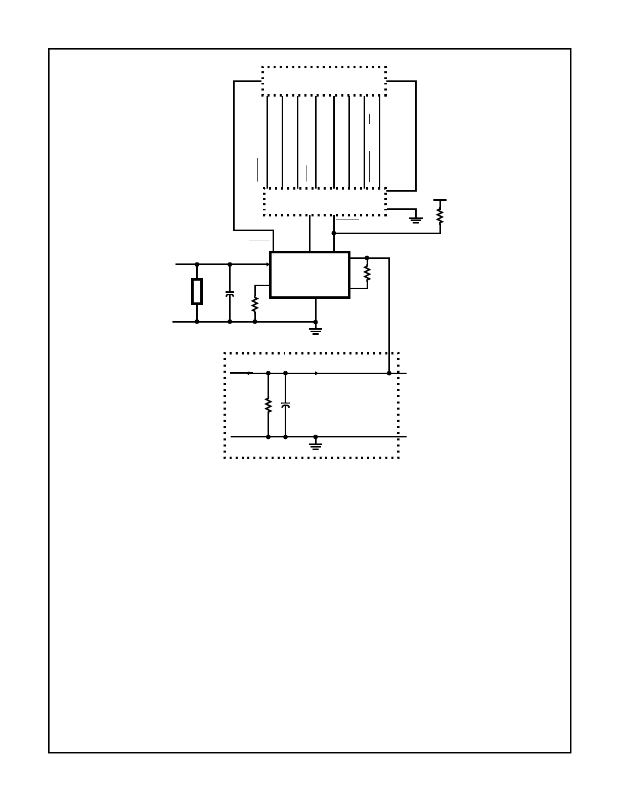
18
HIP7010
FIGURE 8.
0.01
µ
F
C1
M1
HIP7010 BLIC
BUS OUT
BUS IN
BATT
GND
R
F
R
BS
C
BS
R
S
J1850 BUS
RX
TX
J1850 BUS
TRANSCEIVER
43V
R/F
LB EN
MOV
VPWIN
VPWIN
15K
62K
SACTIVE
SIN
SOUT
SCK
SS
MISO
MOSI
SCK
PA
0
PA
1
RDY
ST
A
T
PA
2
RESET
TCAP
IDLE
PA3
OSCOUT
CLK
TEST
+5V
6805 MICROCONTROLLER
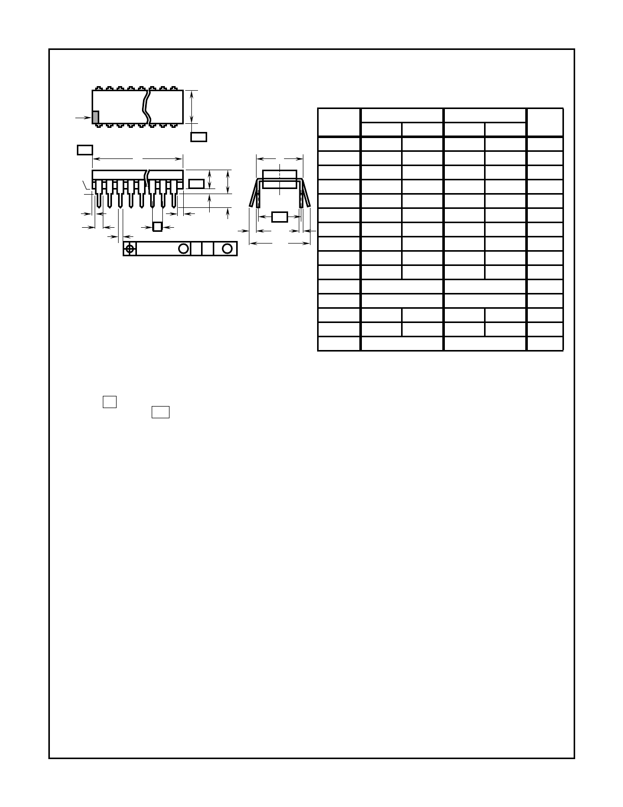
19
HIP7010
NOTES:
1. Controlling Dimensions: INCH. In case of conflict between
English and Metric dimensions, the inch dimensions control.
2. Dimensioning and tolerancing per ANSI Y14.5M-1982.
3. Symbols are defined in the “MO Series Symbol List” in Section
2.2 of Publication No. 95.
4. Dimensions A, A1 and L are measured with the package seated
in JEDEC seating plane gauge GS-3.
5. D, D1, and E1 dimensions do not include mold flash or protru-
sions. Mold flash or protrusions shall not exceed 0.010 inch
(0.25mm).
6. E and
are measured with the leads constrained to be per-
pendicular to datum
.
7. e
B
and e
C
are measured at the lead tips with the leads uncon-
strained. e
C
must be zero or greater.
8. B1 maximum dimensions do not include dambar protrusions.
Dambar protrusions shall not exceed 0.010 inch (0.25mm).
9. N is the maximum number of terminal positions.
10. Corner leads (1, N, N/2 and N/2 + 1) for E8.3, E16.3, E18.3,
E28.3, E42.6 will have a B1 dimension of 0.030 - 0.045 inch
(0.76 - 1.14mm).
C
L
E
e
A
C
e
B
e
C
-B-
E1
INDEX
1 2 3
N/2
N
AREA
SEATING
BASE
PLANE
PLANE
-C-
D1
B1
B
0.010 (0.25)
C
A
M
B S
e
D
D1
A
A2
L
A1
-A-
e
A
-C-
E14.3
(JEDEC MS-001-AA ISSUE D)
14 LEAD DUAL-IN-LINE PLASTIC PACKAGE
SYMBOL
INCHES
MILLIMETERS
NOTES
MIN
MAX
MIN
MAX
A
-
0.210
-
5.33
4
A1
0.015
-
0.39
-
4
A2
0.115
0.195
2.93
4.95
-
B
0.014
0.022
0.356
0.558
-
B1
0.045
0.070
1.15
1.77
8
C
0.008
0.014
0.204
0.355
-
D
0.735
0.775
18.66
19.68
5
D1
0.005
-
0.13
-
5
E
0.300
0.325
7.62
8.25
6
E1
0.240
0.280
6.10
7.11
5
e
0.100 BSC
2.54 BSC
-
e
A
0.300 BSC
7.62 BSC
6
e
B
-
0.430
-
10.92
7
L
0.115
0.150
2.93
3.81
4
N
14
14
9
Rev. 0 12/93
Dual-In-Line Plastic Packages (PDIP)
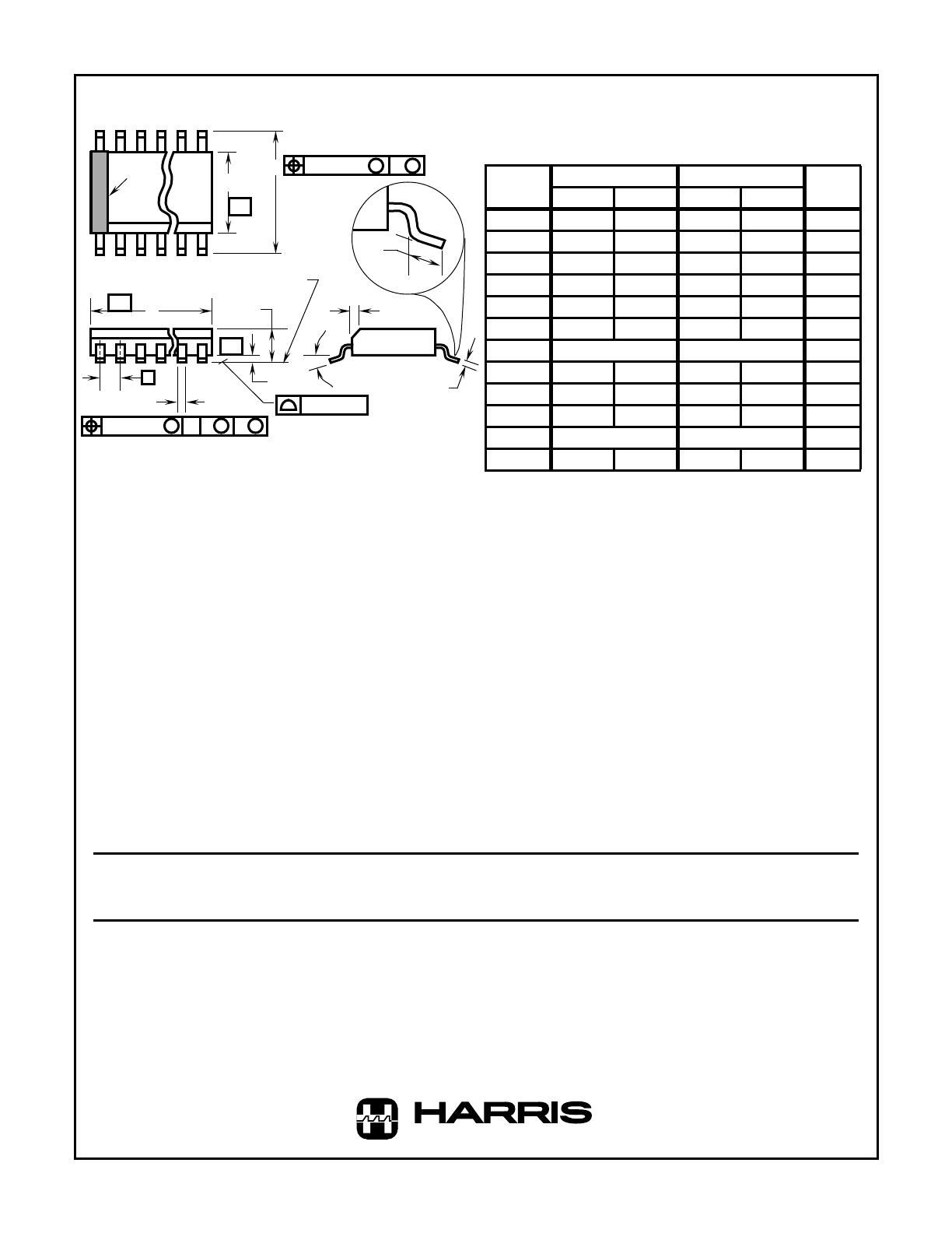
20
Harris Semiconductor products are sold by description only. Harris Semiconductor reserves the right to make changes in circuit design and/or specifications at
any time without notice. Accordingly, the reader is cautioned to verify that data sheets are current before placing orders. Information furnished by Harris is
believed to be accurate and reliable. However, no responsibility is assumed by Harris or its subsidiaries for its use; nor for any infringements of patents or other
rights of third parties which may result from its use. No license is granted by implication or otherwise under any patent or patent rights of Harris or its subsidiaries.
Sales Office Headquarters
For general information regarding Harris Semiconductor and its products, call 1-800-4-HARRIS
UNITED STATES
Harris Semiconductor
P. O. Box 883, Mail Stop 53-210
Melbourne, FL 32902
TEL: 1-800-442-7747
(407) 729-4984
FAX: (407) 729-5321
EUROPE
Harris Semiconductor
Mercure Center
100, Rue de la Fusee
1130 Brussels, Belgium
TEL: (32) 2-724-2111
SOUTH ASIA
Harris Semiconductor H.K. Ltd.
13/F Fourseas Building
208-212 Nathan Road
Tsimshatsui, Kowloon
Hong Kong
TEL: (852) 723-6339
NORTH ASIA
Harris K.K.
Kojimachi-Nakata Bldg. 4F
5-3-5 Kojimachi
Chiyoda-ku, Tokyo 102 Japan
TEL: (81) 3-3265-7571
TEL: (81) 3-3265-7572 (Sales)
S E M I C O N D U C T O R
HIP7010
M14.15
(JEDEC MS-012-AB ISSUE C)
14 LEAD NARROW BODY SMALL OUTLINE PLASTIC PACKAGE
SYMBOL
INCHES
MILLIMETERS
NOTES
MIN
MAX
MIN
MAX
A
0.0532
0.0688
1.35
1.75
-
A1
0.0040
0.0098
0.10
0.25
-
B
0.013
0.020
0.33
0.51
9
C
0.0075
0.0098
0.19
0.25
-
D
0.3367
0.3444
8.55
8.75
3
E
0.1497
0.1574
3.80
4.00
4
e
0.050 BSC
1.27 BSC
-
H
0.2284
0.2440
5.80
6.20
-
h
0.0099
0.0196
0.25
0.50
5
L
0.016
0.050
0.40
1.27
6
N
14
14
7
α
0
o
8
o
0
o
8
o
-
Rev. 0 12/93
NOTES:
1. Symbols are defined in the “MO Series Symbol List” in Section
2.2 of Publication Number 95.
2. Dimensioning and tolerancing per ANSI Y14.5M-1982.
3. Dimension “D” does not include mold flash, protrusions or gate
burrs. Mold flash, protrusion and gate burrs shall not exceed
0.15mm (0.006 inch) per side.
4. Dimension “E” does not include interlead flash or protrusions. In-
terlead flash and protrusions shall not exceed 0.25mm (0.010
inch) per side.
5. The chamfer on the body is optional. If it is not present, a visual
index feature must be located within the crosshatched area.
6. “L” is the length of terminal for soldering to a substrate.
7. “N” is the number of terminal positions.
8. Terminal numbers are shown for reference only.
9. The lead width “B”, as measured 0.36mm (0.014 inch) or greater
above the seating plane, shall not exceed a maximum value of
0.61mm (0.024 inch).
10. Controlling dimension: MILLIMETER. Converted inch dimen-
sions are not necessarily exact.
INDEX
AREA
E
D
N
1
2
3
-B-
0.25(0.010)
C A
M
B S
e
-A-
L
B
M
-C-
A1
A
SEATING PLANE
0.10(0.004)
h x 45
o
C
H
0.25(0.010)
B
M
M
α
Small Outline Plastic Packages (SOIC)