
©2001 Fairchild Semiconductor Corporation
www.fairchildsemi.com
Rev. 1.0.1
Features
• Low input bias current : 250nA (Max)
• Low input offset current : 50nA (Max)
• Differential Input Voltage :
±
30V
• Power supply voltage : single 5.0V supply to
±
15V.
• Offset voltage null capability.
• Strobe capability.
Description
The LM311 series is a monolithic, low input current voltage
comparator. The device is also designed to operate from dual
or single supply voltage.
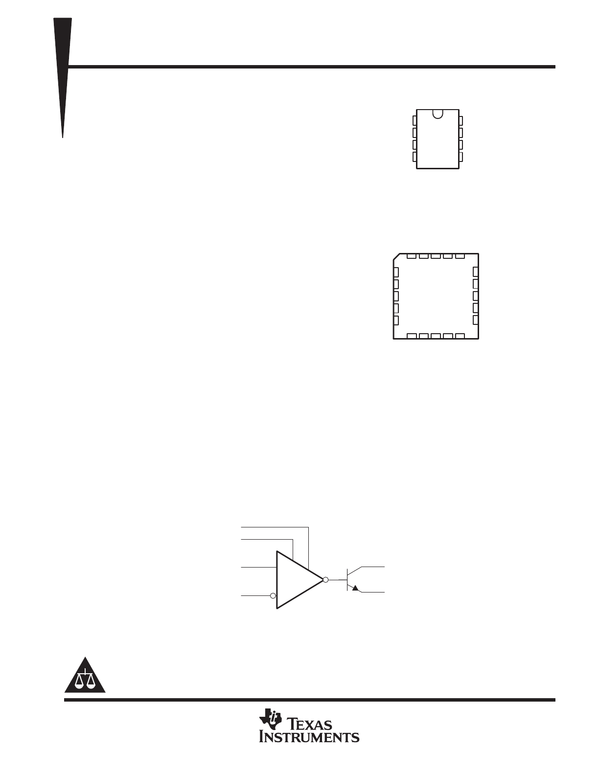
8-DIP
8-SOP
1
1
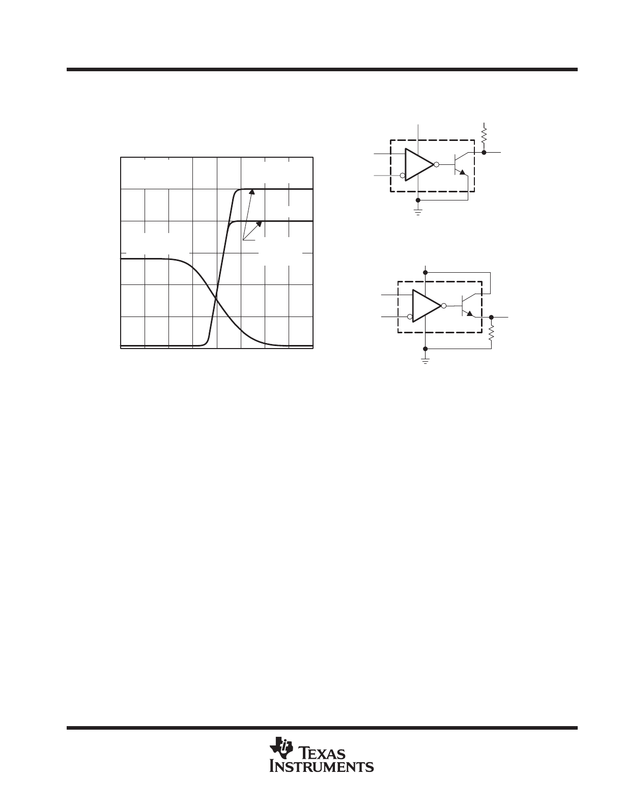
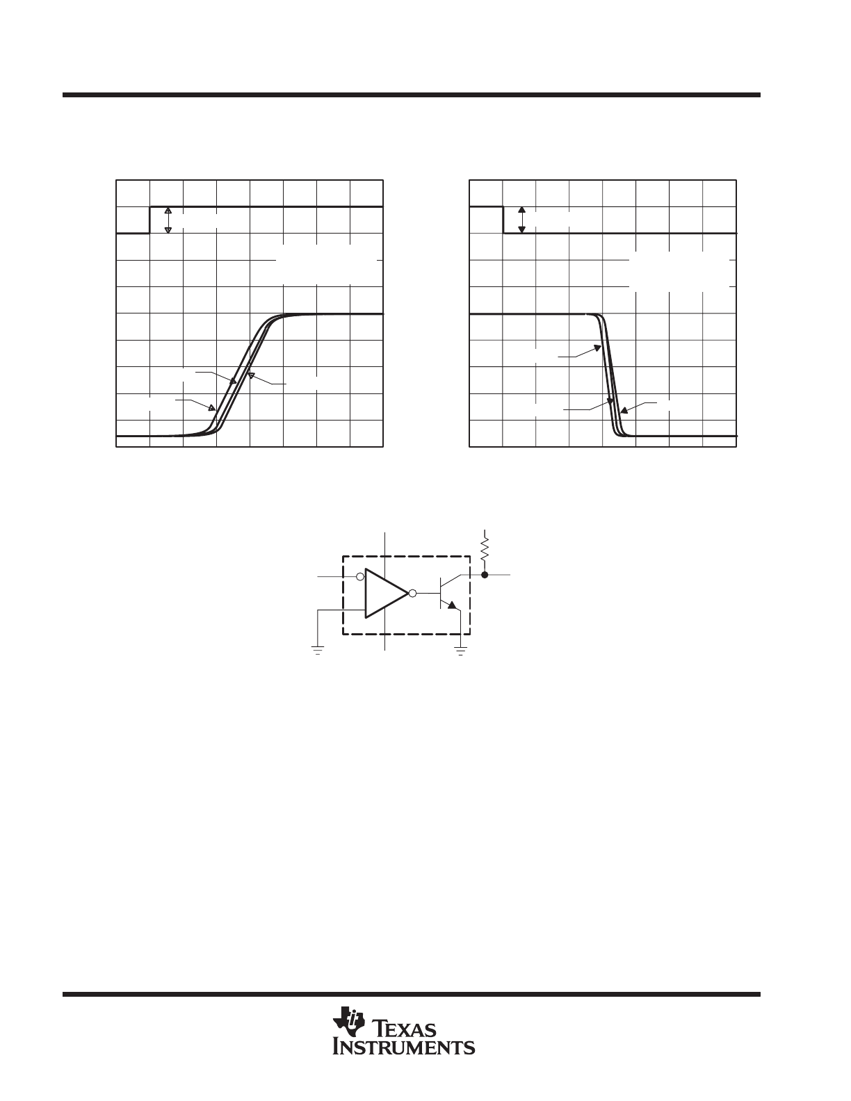
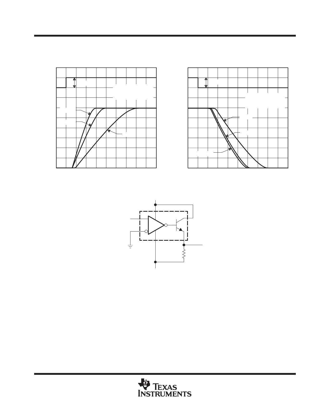
Internal Block Diagram
LM311
Single Comparator
LM311
2
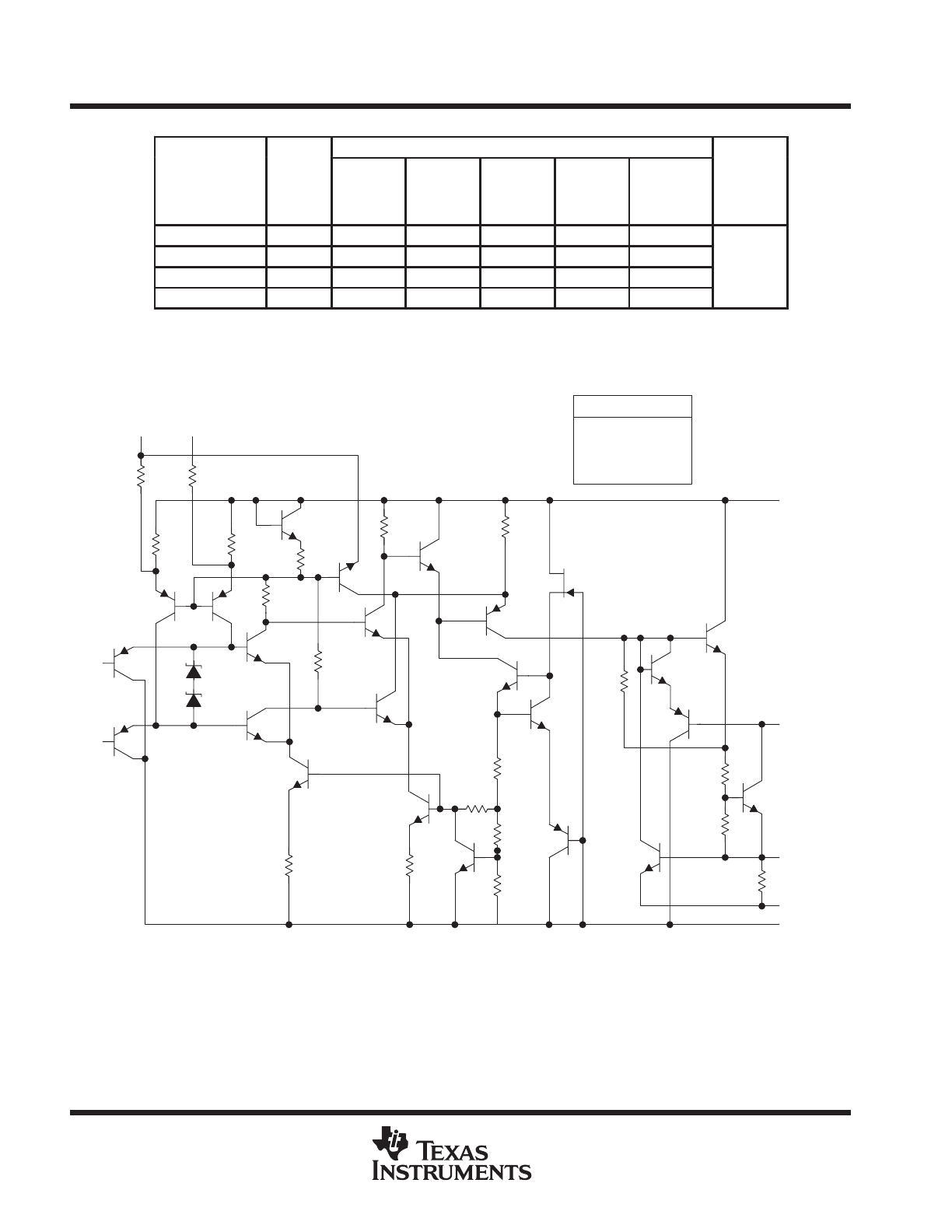
Schematic Diagram
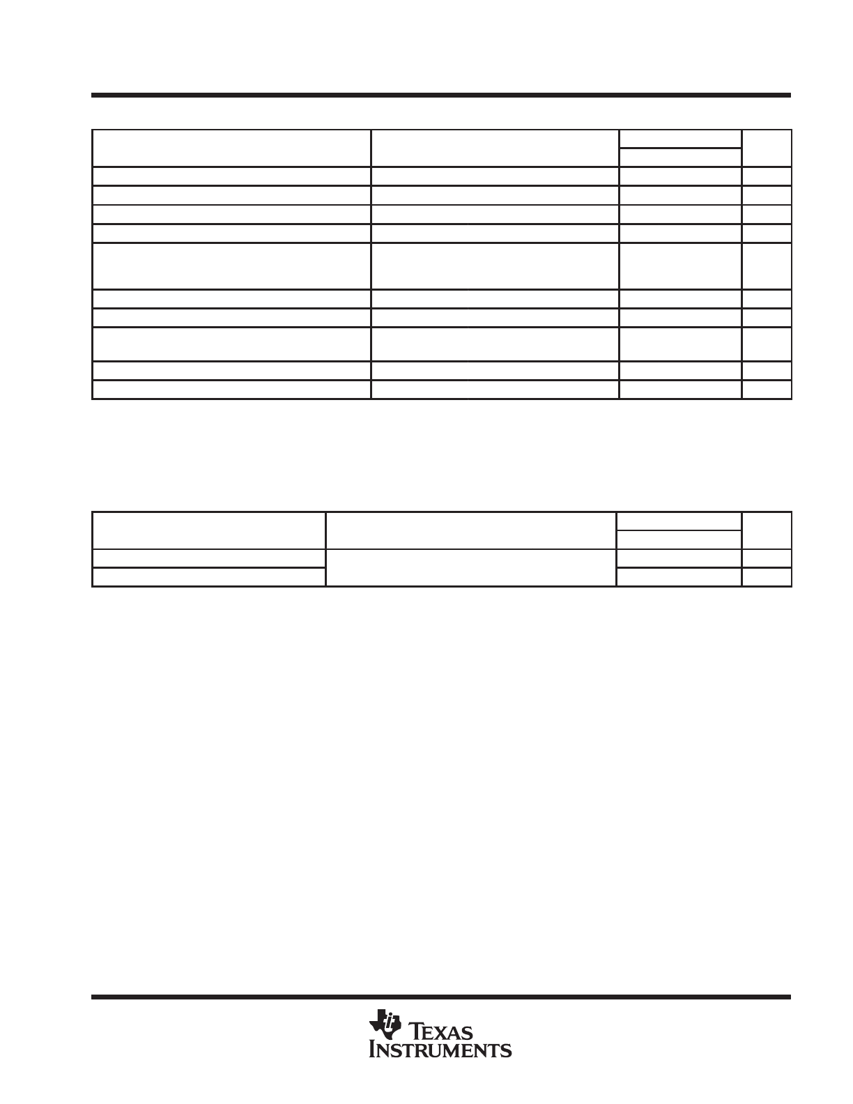
Absolute Maximum Ratings
Parameter
Symbol
Value
Unit
Total Supply Voltage
V
CC
36
V
Output to Negative Supply Voltage LM311
V
O
- V
EE
40
V
Ground to Negative voltage
V
EE
-30
V
Differential Input Voltage
V
I(DIFF)
30
V
Input Voltage
V
I
±
15
V
Output Short Circuit Duration
-
10
sec
Power Dissipation
P
D
500
mW
Operating Temperature Range
T
OPR
0 ~ +70
°
C
Storage Temperature Range
T
STG
- 65 ~ +150
°
C
LM311
3
Electrical Characteristics
(V
CC
= 15V, T
A
= 25
°
C, unless otherwise specified)
Notes :
1. 0
≤
T
A
≤
+70
°
C
2. The response time specified is for a 100mV input step with 5mV over drive.
Parameter
Symbol
Conditions
Min.
Typ.
Max.
Unit
Input Offset Voltage
V
IO
R
S
≤
50K
Ω
-
1.0
7.5
mV
Note 1
-
-
10
Input Offset Current
I
IO
-
6
50
nA
Note 1
-
-
70
Input Bias Current
I
BIAS
-
100
250
nA
Note 1
-
-
300
Voltage Gain
G
V
-
40
200
-
V/mV
Response Time
T
RES
Note 2
-
200
-
ns
Saturation Voltage
V
SAT
I
O
=50mA, V
I
≤
-10mV
-
0.75
1.5
V
V
CC
≥
4.5V, V
EE
=0V
I
O
=8mA, V
I
≤
-10mV, Note 1
-
0.23
0.4
Strobe “ON” Current
I
STR(ON)
-
-
3
-
mA
Output Leakage Current
I
SINK
I
STR
=3mA, V
I
≥
10mV
V
O
=15V, V
CC
=±15V
-
0.2
50
nA
Input Voltage Range
V
I(R)
Note 1
-14.5
to
13.0
-14.7
to
13.8
-
V
Positive Supply Current
I
CC
-
-
3.0
7.5
mA
Negative Supply Current
I
EE
-
-
-2.2
-5.0
mA
Strobe Current
I
STR
-
-
3
-
mA
LM311
4
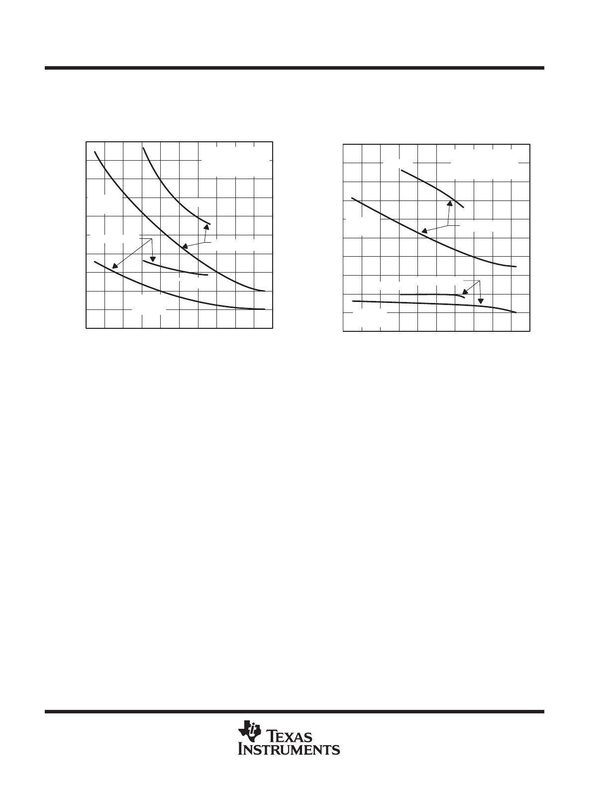
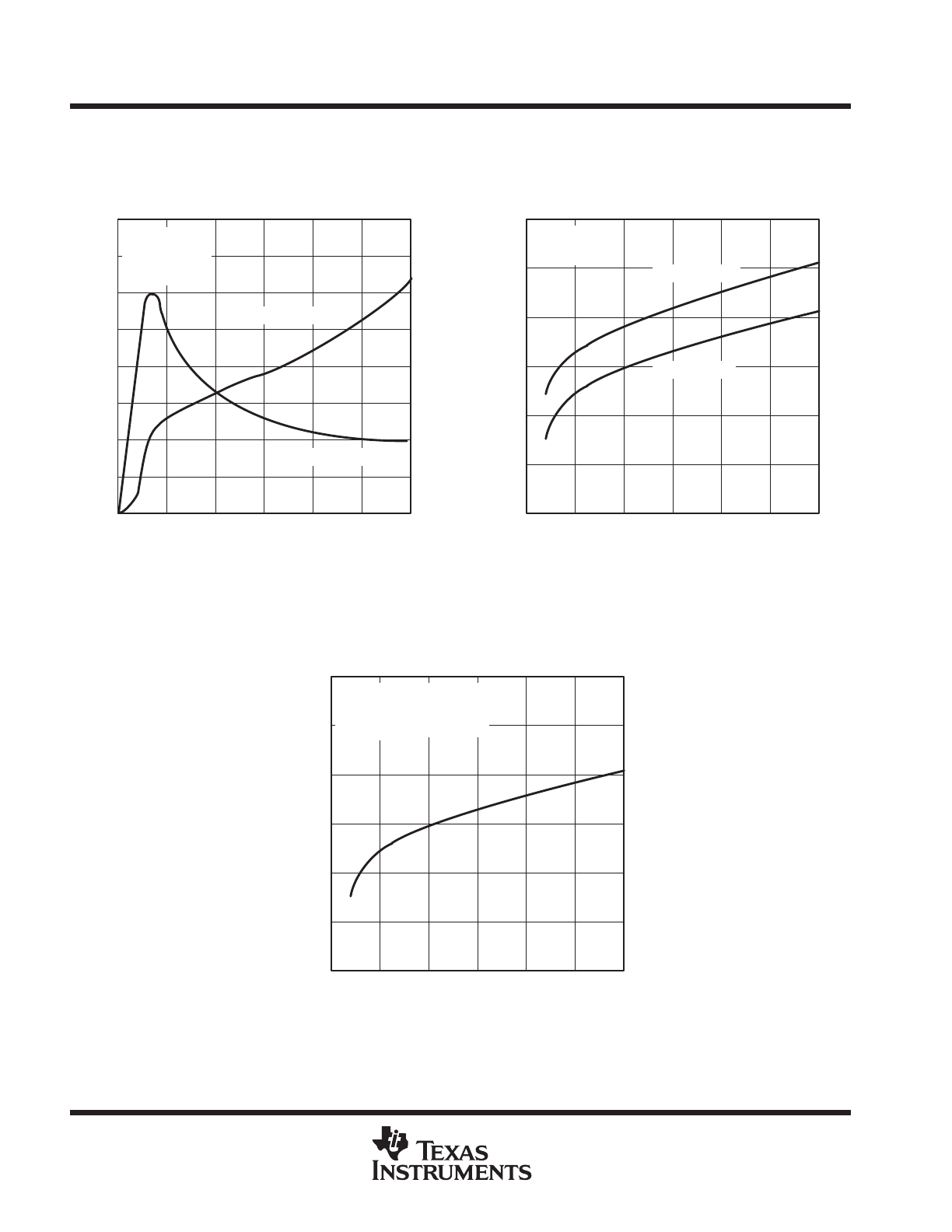
Typical Performance Characteristics
Figure 1. Input Bias Current vs Temperature
Figure 2. Input Offset Current vs Temperature
Figure 3. Offset Voltage vs Input Resistance
Figure 4. Input Bias Current vs
Differential input voltage
Figure 5. Common Mode Limits vs Temperature
Figure 6. Output Voltage vs
Differential input voltage
LM311
5
Typical Performance Characteristics (continued)
Figure 7. Saturation voltage vs Current
Figure 8. Supply Current vs Temperature
Figure 9. Leakage Current vs Temperature
Figure 10. Supply Current vs Supply Voltage
Figure 11. Current Saturation Voltage
Figure 12. Output Limiting Characterstics
LM311
6
Mechanical Dimensions
Package
6.40
±
0.20
3.30
±
0.30
0.130
±
0.012
3.40
±
0.20
0.134
±
0.008
#1
#4
#5
#8
0.252
±
0.008
9.20
±
0.20
0.79
2.54
0.100
0.031
()
0.46
±
0.10
0.018
±
0.004
0.060
±
0.004
1.524
±
0.10
0.362
±
0.008
9.60
0.378
MAX
5.08
0.200
0.33
0.013
7.62
0~15
°
0.300
MAX
MIN
0.25
+0.10
–0.05
0.010
+0.004
–0.002
8-DIP
LM311
7
Mechanical Dimensions
(Continued)
Package
4.92
±
0.20
0.194
±
0.008
0.41
±
0.10
0.016
±
0.004
1.27
0.050
5.72
0.225
1.55
±
0.20
0.061
±
0.008
0.1~0.25
0.004~0.001
6.00
±
0.30
0.236
±
0.012
3.95
±
0.20
0.156
±
0.008
0.50
±
0.20
0.020
±
0.008
5.13
0.202
MAX
#1
#4
#5
0~8
°
#8
0.56
0.022
()
1.80
0.071
MAX0.10
MAX0.004
MAX
MIN
+
0.10
-0.05
0.15
+
0.004
-0.002
0.006
8-SOP
LM311
8
Ordering Information
Product Number
Package
Operating Temperature
LM311N
8-DIP
0 ~ +70
°
C
LM311M
8-SOP
LM311
9
LM311
6/1/01 0.0m 001
Stock#DSxxxxxxxx
2001 Fairchild Semiconductor Corporation
LIFE SUPPORT POLICY
FAIRCHILD’S PRODUCTS ARE NOT AUTHORIZED FOR USE AS CRITICAL COMPONENTS IN LIFE SUPPORT DEVICES
OR SYSTEMS WITHOUT THE EXPRESS WRITTEN APPROVAL OF THE PRESIDENT OF FAIRCHILD SEMICONDUCTOR
CORPORATION. As used herein:
1. Life support devices or systems are devices or systems
which, (a) are intended for surgical implant into the body,
or (b) support or sustain life, and (c) whose failure to
perform when properly used in accordance with
instructions for use provided in the labeling, can be
reasonably expected to result in a significant injury of the
user.
2. A critical component in any component of a life support
device or system whose failure to perform can be
reasonably expected to cause the failure of the life support
device or system, or to affect its safety or effectiveness.
www.fairchildsemi.com
DISCLAIMER
FAIRCHILD SEMICONDUCTOR RESERVES THE RIGHT TO MAKE CHANGES WITHOUT FURTHER NOTICE TO ANY
PRODUCTS HEREIN TO IMPROVE RELIABILITY, FUNCTION OR DESIGN. FAIRCHILD DOES NOT ASSUME ANY
LIABILITY ARISING OUT OF THE APPLICATION OR USE OF ANY PRODUCT OR CIRCUIT DESCRIBED HEREIN; NEITHER
DOES IT CONVEY ANY LICENSE UNDER ITS PATENT RIGHTS, NOR THE RIGHTS OF OTHERS.