
© 2001 Fairchild Semiconductor Corporation
DS006431
www.fairchildsemi.com
April 1986
Revised November 2001
DM74LS373
•
D
M
74LS37
4
3-
ST
A
T
E
Octal
D-
T
y
pe T
ranspar
ent
Lat
c
hes a
nd Edge-
T
ri
ggere
d Fl
ip-
F
lops
DM74LS373 • DM74LS374
3-STATE Octal D-Type Transparent Latches
and Edge-Triggered Flip-Flops
General Description
These 8-bit registers feature totem-pole 3-STATE outputs
designed specifically for driving highly-capacitive or rela-
tively low-impedance loads. The high-impedance state and
increased high-logic level drive provide these registers with
the capability of being connected directly to and driving the
bus lines in a bus-organized system without need for inter-
face or pull-up components. They are particularly attractive
for implementing buffer registers, I/O ports, bidirectional
bus drivers, and working registers.
The eight latches of the DM74LS373 are transparent D-
type latches meaning that while the enable (G) is HIGH the
Q outputs will follow the data (D) inputs. When the enable
is taken LOW the output will be latched at the level of the
data that was set up.
The eight flip-flops of the DM74LS374 are edge-triggered
D-type flip flops. On the positive transition of the clock, the
Q outputs will be set to the logic states that were set up at
the D inputs.
A buffered output control input can be used to place the
eight outputs in either a normal logic state (HIGH or LOW
logic levels) or a high-impedance state. In the high-imped-
ance state the outputs neither load nor drive the bus lines
significantly.
The output control does not affect the internal operation of
the latches or flip-flops. That is, the old data can be
retained or new data can be entered even while the outputs
are OFF.
Features
■
Choice of 8 latches or 8 D-type flip-flops in a single
package
■
3-STATE bus-driving outputs
■
Full parallel-access for loading
■
Buffered control inputs
■
P-N-P inputs reduce D-C loading on data lines
Ordering Code:
Devices also available in Tape and Reel. Specify by appending the suffix letter “X” to the ordering code.
Order Number
Package Number
Package Description
DM74LS373WM
M20B
20-Lead Small Outline Integrated Circuit (SOIC), JEDEC MS-013, 0.300" Wide
DM74LS373SJ
M20D
20-Lead Small Outline Package (SOP), EIAJ TYPE II, 5.3mm Wide
DM74LS373N
N20A
20-Lead Plastic Dual-In-Line Package (PDIP), JEDEC MS-001, 0.300" Wide
DM74LS374WM
M20B
20-Lead Small Outline Integrated Circuit (SOIC), JEDEC MS-013, 0.300" Wide
DM74LS374SJ
M20D
20-Lead Small Outline Package (SOP), EIAJ TYPE II, 5.3mm Wide
DM74LS374N
N20A
20-Lead Plastic Dual-In-Line Package (PDIP), JEDEC MS-001, 0.300" Wide
www.fairchildsemi.com
2
DM74LS373
• DM74LS374
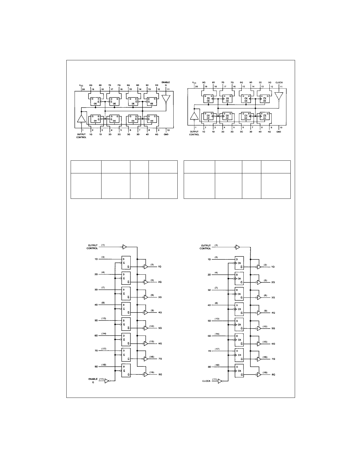
Connection Diagrams
DM74LS373
DM74LS374
Function Tables
DM74LS373
DM74LS374
H
=
HIGH Level (Steady State)
L
=
LOW Level (Steady State)
X
=
Don’t Care
Z
=
High Impedance State
↑
=
Transition from LOW-to-HIGH level
Q
0
=
The level of the output
before steady-state input conditions were established.
Logic Diagrams
DM74LS373
Transparent Latches
DM74LS374
Positive-Edge-Triggered Flip-Flops
Output
Enable
D
Output
Control
G
L
H
H
H
L
H
L
L
L
L
X
Q
0
H
X
X
Z
Output
Clock
D
Output
Control
L
↑
H
H
L
↑
L
L
L
L
X
Q
0
H
X
X
Z
3
www.fairchildsemi.com
DM74LS373
•
D
M
74LS37
4
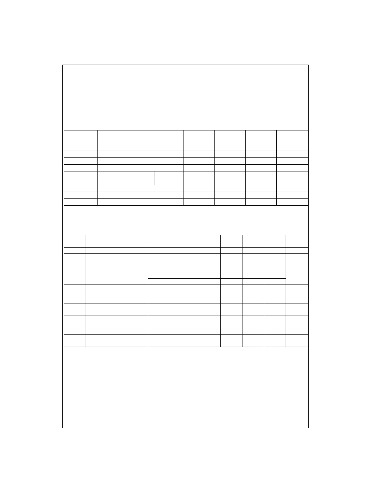
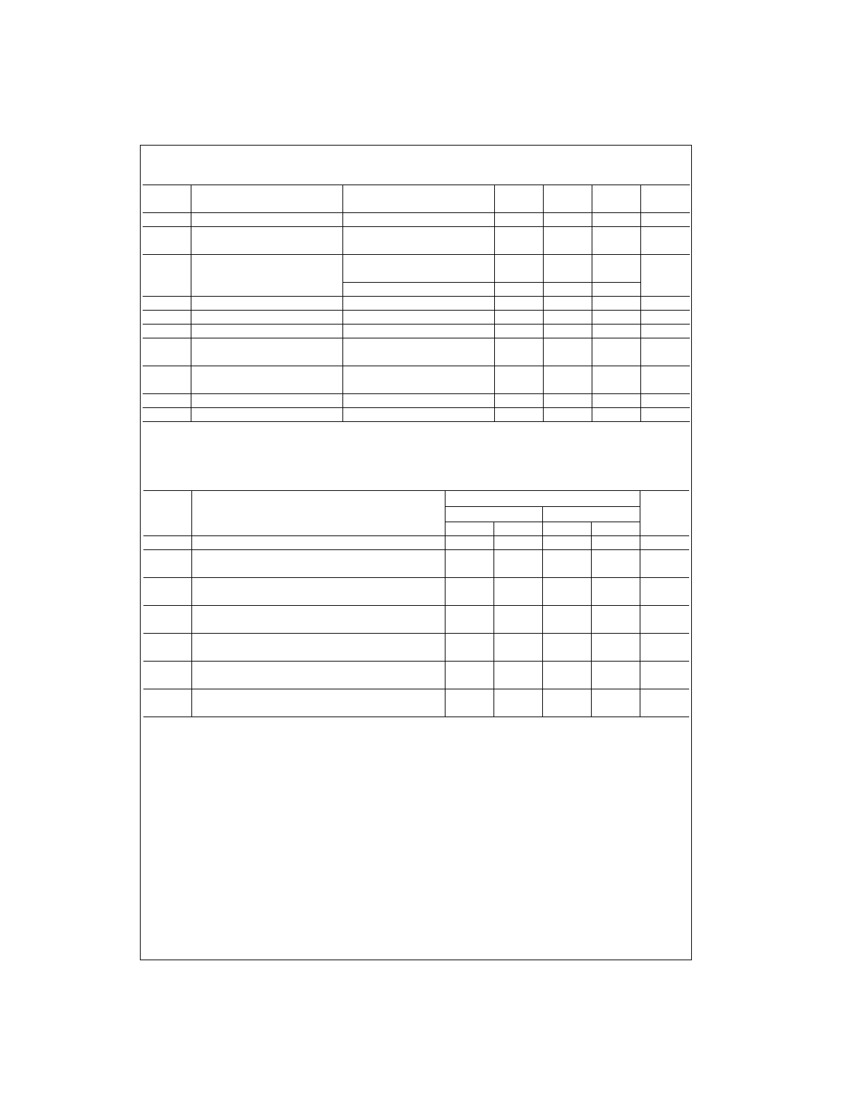
Absolute Maximum Ratings
(Note 1)
Note 1: The “Absolute Maximum Ratings” are those values beyond which
the safety of the device cannot be guaranteed. The device should not be
operated at these limits. The parametric values defined in the Electrical
Characteristics tables are not guaranteed at the absolute maximum ratings.
The “Recommended Operating Conditions” table will define the conditions
for actual device operation.
DM74LS373 Recommended Operating Conditions
Note 2: The symbol (
↓
) indicates the falling edge of the clock pulse is used for reference.
Note 3: T
A
=
25
°
C and V
CC
=
5V.
DM74LS373 Electrical Characteristics
over recommended operating free air temperature range (unless otherwise noted)
Note 4: All typicals are at V
CC
=
5V, T
A
=
25
°
C.
Note 5: Not more than one output should be shorted at a time, and the duration should not exceed one second.
Supply Voltage
7V
Input Voltage
7V
Storage Temperature Range
−
65
°
C to
+
150
°
C
Operating Free Air Temperature Range
0
°
C to
+
70
°
C
Symbol
Parameter
Min
Nom
Max
Units
V
CC
Supply Voltage
4.75
5
5.25
V
V
IH
HIGH Level Input Voltage
2
V
V
IL
LOW Level Input Voltage
0.8
V
I
OH
HIGH Level Output Current
−
2.6
mA
I
OL
LOW Level Output Current
24
mA
t
W
Pulse Width
Enable HIGH
15
ns
(Note 3)
Enable LOW
15
t
SU
Data Setup Time (Note 2) (Note 3)
5
↓
ns
t
H
Data Hold Time (Note 2) (Note 3)
20
↓
ns
T
A
Free Air Operating Temperature
0
70
°
C
Symbol
Parameter
Conditions
Min
Typ
Max
Units
(Note 4)
V
I
Input Clamp Voltage
V
CC
=
Min, I
I
=
−
18 mA
−
1.5
V
V
OH
HIGH Level
V
CC
=
Min, I
OH
=
Max
2.4
3.1
V
Output Voltage
V
IL
=
Max, V
IH
=
Min
V
OL
LOW Level
V
CC
=
Min, I
OL
=
Max
Output Voltage
V
IL
=
Max, V
IH
=
Min
0.35
0.5
V
I
OL
=
12 mA, V
CC
=
Min
0.4
I
I
Input Current @ Max Input Voltage
V
CC
=
Max, V
I
=
7V
0.1
mA
I
IH
HIGH Level Input Current
V
CC
=
Max, V
I
=
2.7V
20
µ
A
I
IL
LOW Level Input Current
V
CC
=
Max, V
I
=
0.4V
−
0.4
mA
I
OZH
Off-State Output Current with
V
CC
=
Max, V
O
=
2.7V
20
µ
A
HIGH Level Output Voltage Applied
V
IH
=
Min, V
IL
=
Max
I
OZL
Off-State Output Current with
V
CC
=
Max, V
O
=
0.4V
−
20
µ
A
LOW Level Output Voltage Applied
V
IH
=
Min, V
IL
=
Max
I
OS
Short Circuit Output Current
V
CC
=
Max (Note 5)
−
50
−
225
mA
I
CC
Supply Current
V
CC
=
Max, OC
=
4.5V,
24
40
mA
D
n
, Enable
=
GND
www.fairchildsemi.com
4
DM74LS373
• DM74LS374
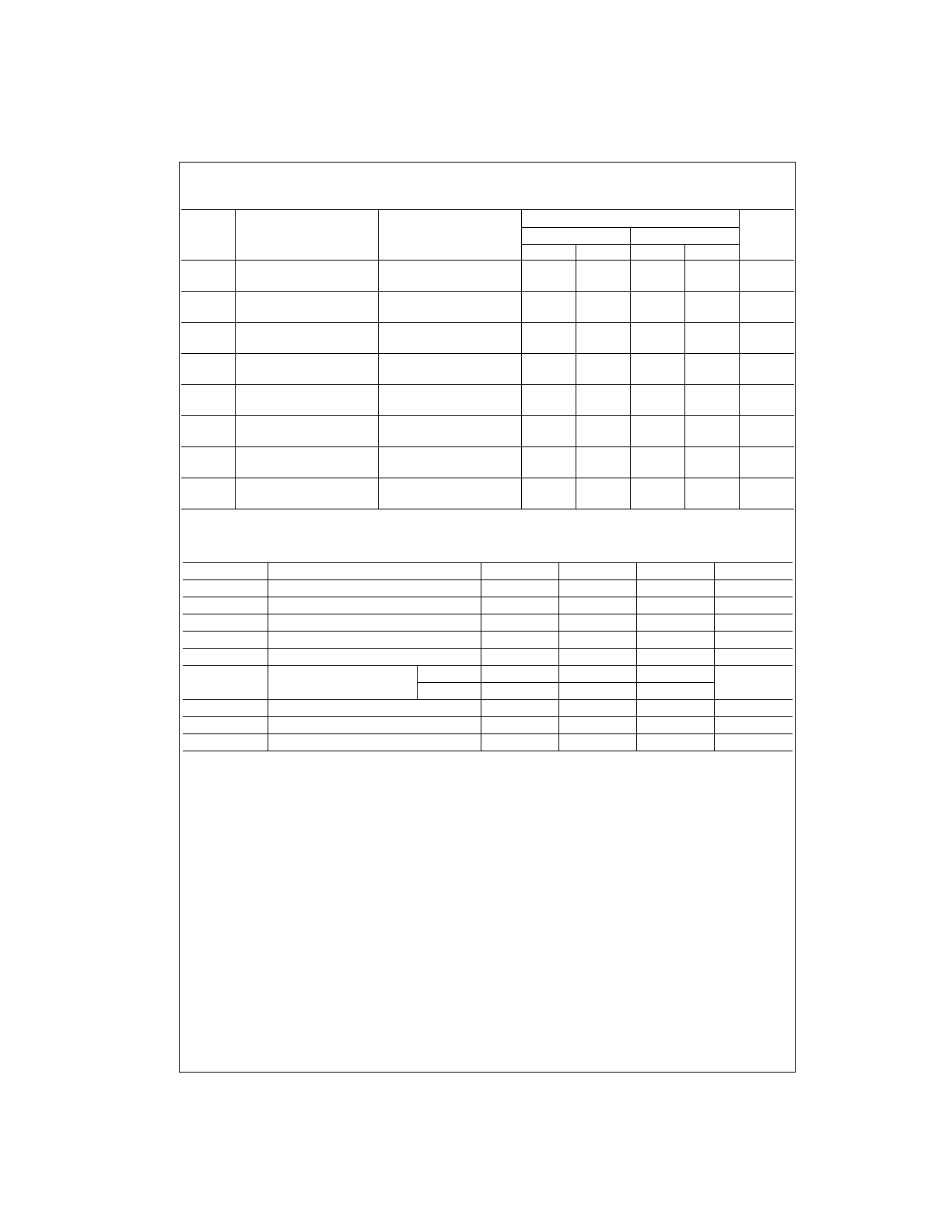
DM74LS373 Switching Characteristics
at V
CC
=
5V and T
A
=
25
°
C
Note 6: C
L
=
5 pF.
DM74LS374 Recommended Operating Conditions
Note 7: The symbol (
↑
) indicates the rising edge of the clock pulse is used for reference.
Note 8: T
A
=
25
°
C and V
CC
=
5V.
R
L
=
667
Ω
Symbol
Parameter
From (Input)
C
L
=
45 pF
C
L
=
150 pF
Units
To (Output)
Min
Max
Min
Max
t
PLH
Propagation Delay Time
Data to Q
18
26
ns
LOW-to-HIGH Level Output
t
PHL
Propagation Delay Time
Data to Q
18
27
ns
HIGH-to-LOW Level Output
t
PLH
Propagation Delay Time
Enable to Q
30
38
ns
LOW-to-HIGH Level Output
t
PHL
Propagation Delay Time
Enable to Q
30
36
ns
HIGH-to-LOW Level Output
t
PZH
Output Enable Time
Output Control to Any Q
28
36
ns
to HIGH Level Output
t
PZL
Output Enable Time
Output Control to Any Q
36
50
ns
to LOW Level Output
t
PHZ
Output Disable Time
Output Control to Any Q
20
ns
from HIGH Level Output (Note 6)
t
PLZ
Output Disable Time
Output Control to Any Q
25
ns
from LOW Level Output (Note 6)
Symbol
Parameter
Min
Nom
Max
Units
V
CC
Supply Voltage
4.75
5
5.25
V
V
IH
HIGH Level Input Voltage
2
V
V
IL
LOW Level Input Voltage
0.8
V
I
OH
HIGH Level Output Current
−
2.6
mA
I
OL
LOW Level Output Current
24
mA
t
W
Pulse Width
Clock HIGH
15
ns
(Note 8)
Clock LOW
15
t
SU
Data Setup Time (Note 7) (Note 8)
20
↑
ns
t
H
Data Hold Time (Note 7) (Note 8)
1
↑
ns
T
A
Free Air Operating Temperature
0
70
°
C
5
www.fairchildsemi.com
DM74LS373
•
D
M
74LS37
4
DM74LS374 Electrical Characteristics
over recommended operating free air temperature range (unless otherwise noted)
Note 9: All typicals are at V
CC
=
5V, T
A
=
25
°
C.
Note 10: Not more than one output should be shorted at a time, and the duration should not exceed one second.
DM74LS374 Switching Characteristics
at V
CC
=
5V and T
A
=
25
°
C
Note 11: C
L
=
5 pF.
Symbol
Parameter
Conditions
Min
Typ
Max
Units
(Note 9)
V
I
Input Clamp Voltage
V
CC
=
Min, I
I
=
−
18 mA
−
1.5
V
V
OH
HIGH Level
V
CC
=
Min, I
OH
=
Max
2.4
3.1
V
Output Voltage
V
IL
=
Max, V
IH
=
Min
V
OL
LOW Level
V
CC
=
Min, I
OL
=
Max
0.35
0.5
V
Output Voltage
V
IL
=
Max, V
IH
=
Min
I
OL
=
12 mA, V
CC
=
Min
0.25
0.4
I
I
Input Current @ Max Input Voltage
V
CC
=
Max, V
I
=
7V
0.1
mA
I
IH
HIGH Level Input Current
V
CC
=
Max, V
I
=
2.7V
20
µ
A
I
IL
LOW Level Input Current
V
CC
=
Max, V
I
=
0.4V
−
0.4
mA
I
OZH
Off-State Output Current with
V
CC
=
Max, V
O
=
2.7V
20
µ
A
HIGH Level Output Voltage Applied
V
IH
=
Min, V
IL
=
Max
I
OZL
Off-State Output Current with
V
CC
=
Max, V
O
=
0.4V
−
20
µ
A
LOW Level Output Voltage Applied
V
IH
=
Min, V
IL
=
Max
I
OS
Short Circuit Output Current
V
CC
=
Max (Note 10)
−
50
−
225
mA
I
CC
Supply Current
V
CC
=
Max, D
n
=
GND, OC
=
4.5V
27
45
mA
R
L
=
667
Ω
Symbol
Parameter
C
L
=
45 pF
C
L
=
150 pF
Units
Min
Max
Min
Max
f
MAX
Maximum Clock Frequency
35
20
MHz
t
PLH
Propagation Delay Time
28
32
ns
LOW-to-HIGH Level Output
t
PHL
Propagation Delay Time
28
38
ns
HIGH-to-LOW Level Output
t
PZH
Output Enable Time
28
44
ns
to HIGH Level Output
t
PZL
Output Enable Time
28
44
ns
to LOW Level Output
t
PHZ
Output Disable Time
20
ns
from HIGH Level Output (Note 11)
t
PLZ
Output Disable Time
25
ns
from LOW Level Output (Note 11)
www.fairchildsemi.com
6
DM74LS373
• DM74LS374
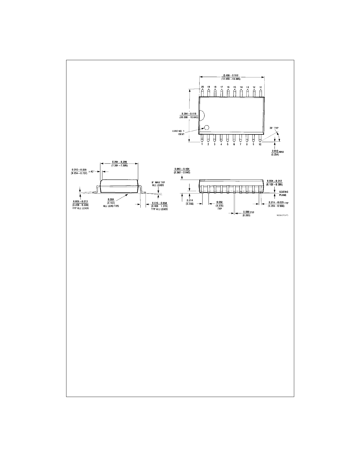
Physical Dimensions
inches (millimeters) unless otherwise noted
20-Lead Small Outline Integrated Circuit (SOIC), JEDEC MS-013, 0.300" Wide
Package Number M20B
7
www.fairchildsemi.com
DM74LS373
•
D
M
74LS37
4
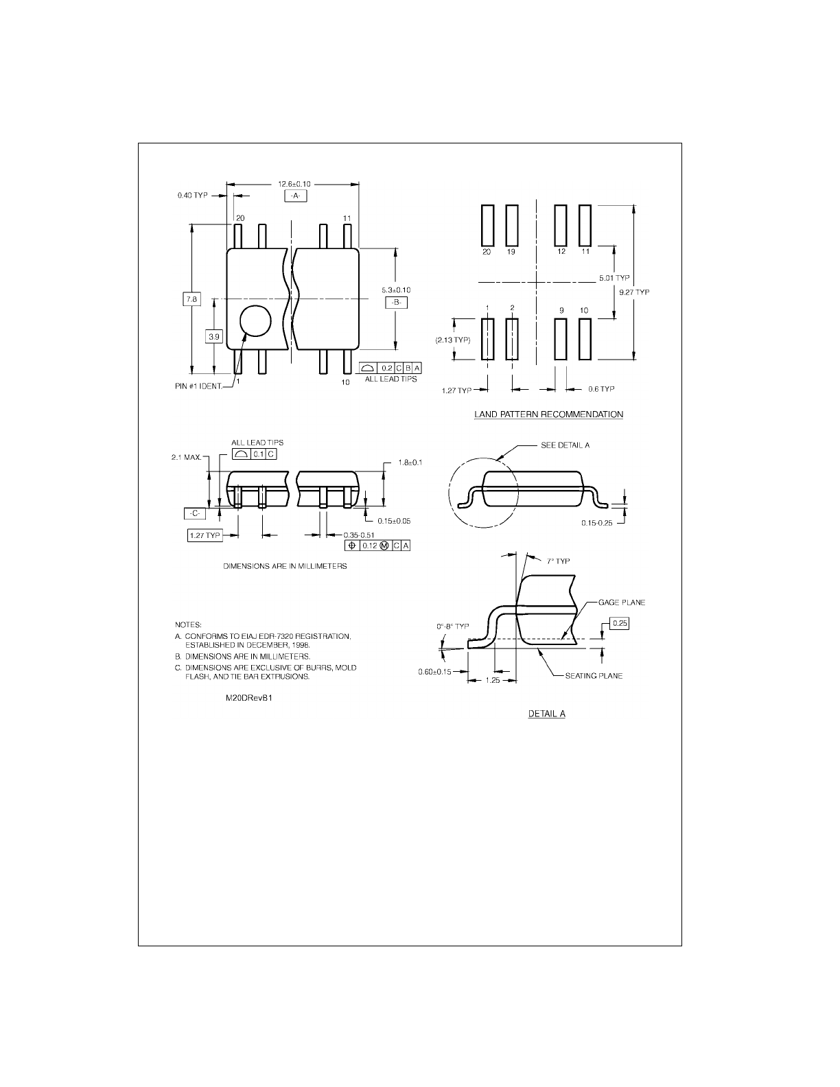
Physical Dimensions
inches (millimeters) unless otherwise noted (Continued)
20-Lead Small Outline Package (SOP), EIAJ TYPE II, 5.3mm Wide
Package Number M20D
www.fairchildsemi.com
8
DM74LS373
• DM74LS374
3-
ST
A
T
E
O
c
tal
D-
T
y
pe T
ranspar
ent
Latch
es and
Edge-
T
ri
ggered
Fl
ip-
F
lops
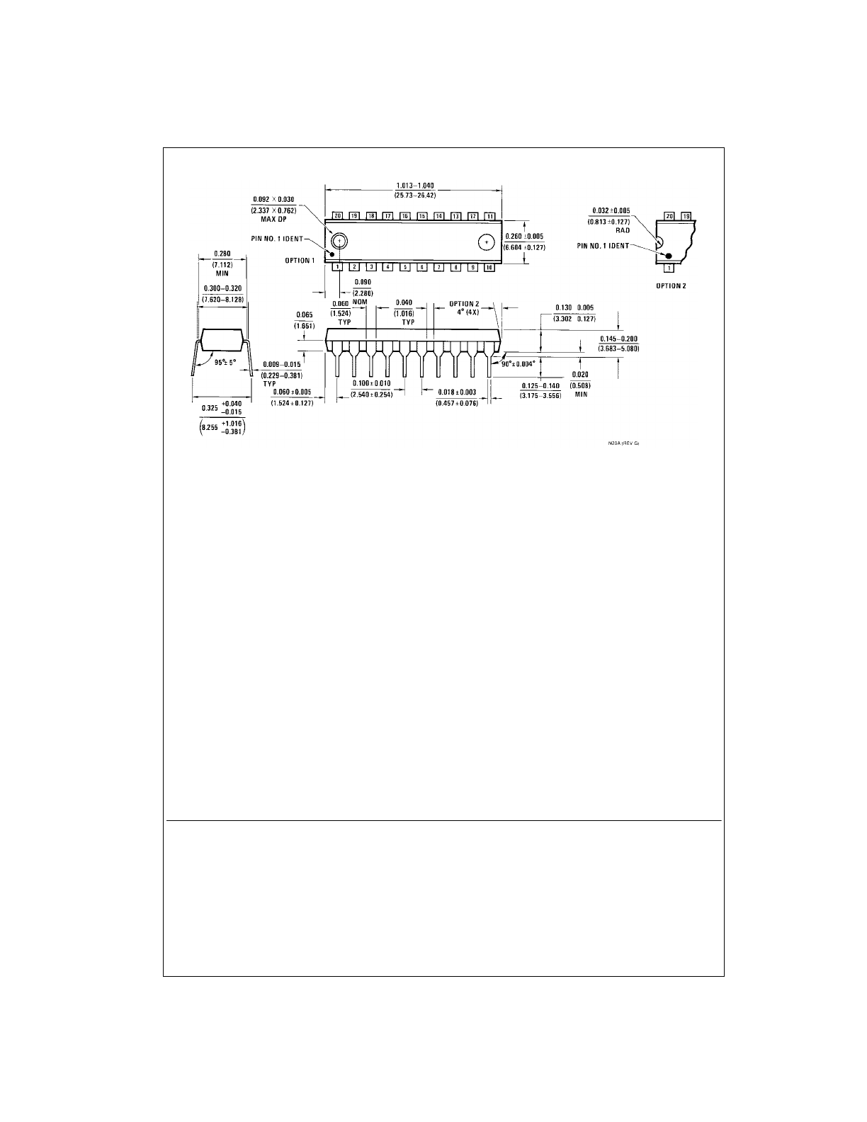
Physical Dimensions
inches (millimeters) unless otherwise noted (Continued)
20-Lead Plastic Dual-In-Line Package (PDIP), JEDEC MS-001, 0.300" Wide
Package Number N20A
Fairchild does not assume any responsibility for use of any circuitry described, no circuit patent licenses are implied and
Fairchild reserves the right at any time without notice to change said circuitry and specifications.
LIFE SUPPORT POLICY
FAIRCHILD’S PRODUCTS ARE NOT AUTHORIZED FOR USE AS CRITICAL COMPONENTS IN LIFE SUPPORT
DEVICES OR SYSTEMS WITHOUT THE EXPRESS WRITTEN APPROVAL OF THE PRESIDENT OF FAIRCHILD
SEMICONDUCTOR CORPORATION. As used herein:
1. Life support devices or systems are devices or systems
which, (a) are intended for surgical implant into the
body, or (b) support or sustain life, and (c) whose failure
to perform when properly used in accordance with
instructions for use provided in the labeling, can be rea-
sonably expected to result in a significant injury to the
user.
2. A critical component in any component of a life support
device or system whose failure to perform can be rea-
sonably expected to cause the failure of the life support
device or system, or to affect its safety or effectiveness.
www.fairchildsemi.com