
© 2000 Fairchild Semiconductor Corporation
DS009825
www.fairchildsemi.com
October 1988
Revised March 2000
DM74LS273
8-
Bit
Regi
ster
wi
th
Clear
DM74LS273
8-Bit Register with Clear
General Description
The DM74LS273 is a high speed 8-bit register, consisting
of eight D-type flip-flops with a common Clock and an
asynchronous active LOW Master Reset. This device is
supplied in a 20-pin package featuring 0.3 inch row spac-
ing.
Features
■
Edge-triggered
■
8-bit high speed register
■
Parallel in and out
■
Common clock and master reset
Ordering Code:
Devices also available in Tape and Reel. Specify by appending the suffix letter “X” to the ordering code.
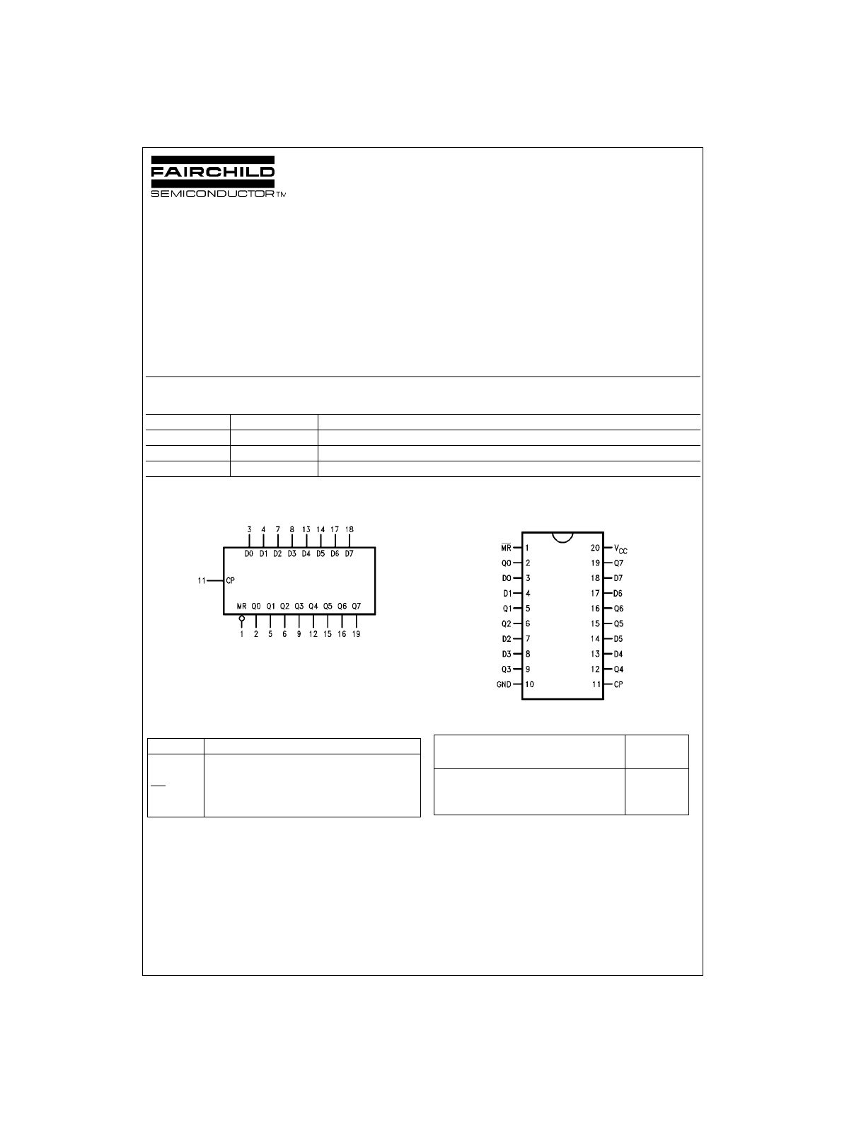
Logic Symbol
V
CC
=
Pin 20
GND
=
Pin 10
Pin Descriptions
Connection Diagram
Truth Table
H
=
HIGH Voltage Level
L
=
LOW Voltage Level
X
=
Immaterial
Order Number
Package Number
Package Description
DM74LS273WM
M20B
20-Lead Small Outline Integrated Circuit (SOIC), JEDEC MS-013, 0.300 Wide
DM74LS273SJ
M20D
20-Lead Small Outline Package (SOP), EIAJ TYPE II, 5.3mm Wide
DM74LS273N
N20A
20-Lead Plastic Dual-In-Line Package (PDIP), JEDEC MS-001, 0.300 Wide
Pin Names
Description
CP
Clock Pulse Input (Active Rising Edge)
D0–D7
Data Inputs
MR
Asynchronous Master Reset Input (Active LOW)
Q0–Q7
Flip-Flop Outputs
Inputs
Outputs
MR
CP
D
n
Q
n
L
X
X
L
H
H
H
H
L
L
www.fairchildsemi.com
2
DM74LS273
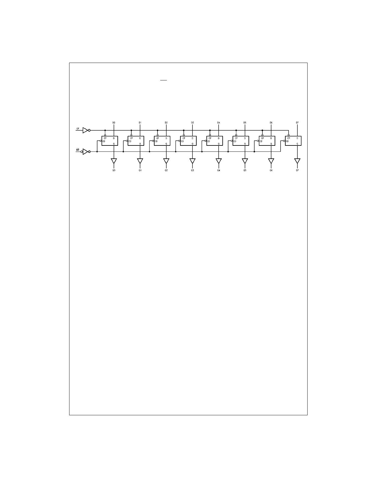
Functional Description
The DM74LS273 is an 8-bit parallel register with a common
Clock and common Master Reset. When the MR input is
LOW, the Q outputs are LOW, independent of the other
inputs. Information meeting the setup and hold time
requirements of the D inputs is transferred to the Q outputs
on the LOW-to-HIGH transition of the clock input.
Logic Diagram
3
www.fairchildsemi.com
DM74LS273
Absolute Maximum Ratings
(Note 1)
Note 1: The “Absolute Maximum Ratings” are those values beyond which
the safety of the device cannot be guaranteed. The device should not be
operated at these limits. The parametric values defined in the Electrical
Characteristics tables are not guaranteed at the absolute maximum ratings.
The “Recommended Operating Conditions” table will define the conditions
for actual device operation.
Recommended Operating Conditions
Electrical Characteristics
Over recommended operating free air temperature range (unless otherwise noted)
Note 2: All typicals are at V
CC
=
5V, T
A
=
25
°
C.
Note 3: Not more than one output should be shorted at a time, and the duration should not exceed one second.
Switching Characteristics
V
CC
=
+
5.0V, T
A
=+
25
°
C
Supply Voltage
7V
Input Voltage
7V
Operating Free Air Temperature Range
0
°
C to
+
70
°
C
Storage Temperature Range
−
65
°
C to
+
150
°
C
Symbol
Parameter
Min
Nom
Max
Units
V
CC
Supply Voltage
4.75
5
5.25
V
V
IH
HIGH Level Input Voltage
2
V
V
IL
LOW Level Input Voltage
0.8
V
I
OH
HIGH Level Output Current
−
0.4
mA
I
OL
LOW Level Output Current
8
mA
T
A
Free Air Operating Temperature
0
70
°
C
t
S
(H)
Setup Time HIGH or LOW
15
ns
t
S
(L)
D
n
to CP
15
t
H
(H)
Hold Time HIGH or LOW
5
ns
t
H
(L)
D
n
to CP
5
t
W
(H)
CP Pulse Width HIGH or LOW
20
ns
t
W
(L)
20
t
W
(L)
MR Pulse Width LOW
20
ns
t
REC
Recovery Time
15
ns
MR to CP
Symbol
Parameter
Conditions
Min
Typ
Max
Units
(Note 2)
V
I
Input Clamp Voltage
V
CC
=
Min, I
I
=
−
18 mA
−
1.5
V
V
OH
HIGH Level
V
CC
=
Min, I
OH
=
Max,
2.7
3.4
V
Output Voltage
V
IL
=
Max
V
OL
LOW
Level V
CC
=
Min, I
OL
=
Max,
0.35
0.5
Output Voltage
V
IH
=
Min
V
I
OL
=
4 mA, V
CC
=
Min
0.25
0.4
I
I
Input Current @ Max Input Voltage
V
CC
=
Max, V
I
=
7V
0.1
mA
I
IH
HIGH Level Input Current
V
CC
=
Max, V
I
=
2.7V
20
µ
A
I
IL
LOW Level Input Current
V
CC
=
Max, V
I
=
0.4V
−
0.4
mA
I
OS
Short Circuit Output Current
V
CC
=
Max (Note 3)
−
20
−
100
mA
I
CC
Supply Current
V
CC
=
Max
27
mA
Symbol
Parameter
C
L
=
15 pF
Units
R
L
=
2 k
Ω
Min
Max
f
MAX
Maximum Clock Frequency
30
MHz
t
PLH
Propagation Delay
24
ns
t
PHL
CP to Q
n
24
t
PLH
Propagation Delay
27
ns
MR to Q
n
www.fairchildsemi.com
4
DM74LS273
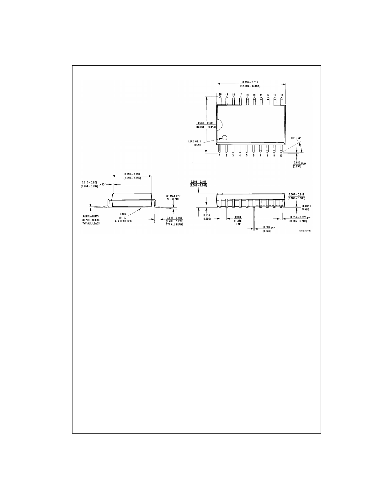
Physical Dimensions
inches (millimeters) unless otherwise noted
20-Lead Small Outline Integrated Circuit (SOIC), JEDEC MS-013, 0.300 Wide
Package Number M20B
5
www.fairchildsemi.com
DM74LS273
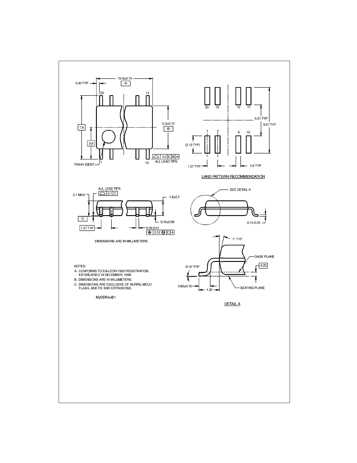
Physical Dimensions
inches (millimeters) unless otherwise noted (Continued)
20-Lead Small Outline Package (SOP), EIAJ TYPE II, 5.3mm Wide
Package Number M20D
www.fairchildsemi.com
6
DM74LS273 8-Bi
t Regis
ter
wit
h
C
lear
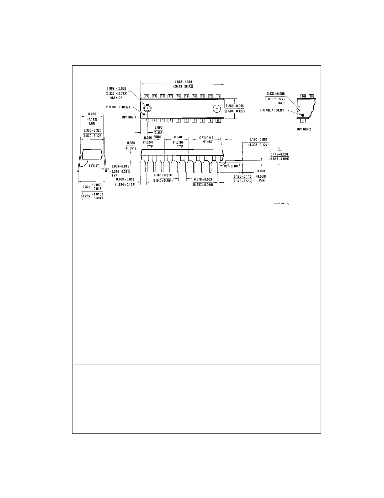
Physical Dimensions
inches (millimeters) unless otherwise noted (Continued)
20-Lead Plastic Dual-In-Line Package (PDIP), JEDEC MS-001, 0.300 Wide
Package Number N20A
Fairchild does not assume any responsibility for use of any circuitry described, no circuit patent licenses are implied and
Fairchild reserves the right at any time without notice to change said circuitry and specifications.
LIFE SUPPORT POLICY
FAIRCHILD’S PRODUCTS ARE NOT AUTHORIZED FOR USE AS CRITICAL COMPONENTS IN LIFE SUPPORT
DEVICES OR SYSTEMS WITHOUT THE EXPRESS WRITTEN APPROVAL OF THE PRESIDENT OF FAIRCHILD
SEMICONDUCTOR CORPORATION. As used herein:
1. Life support devices or systems are devices or systems
which, (a) are intended for surgical implant into the
body, or (b) support or sustain life, and (c) whose failure
to perform when properly used in accordance with
instructions for use provided in the labeling, can be rea-
sonably expected to result in a significant injury to the
user.
2. A critical component in any component of a life support
device or system whose failure to perform can be rea-
sonably expected to cause the failure of the life support
device or system, or to affect its safety or effectiveness.
www.fairchildsemi.com