
© 2000 Fairchild Semiconductor Corporation
DS006418
www.fairchildsemi.com
August 1986
Revised March 2000
DM74LS259
8-
Bit
Addr
essabl
e Lat
ches
DM74LS259
8-Bit Addressable Latches
General Description
These 8-bit addressable latches are designed for general
purpose storage applications in digital systems. Specific
uses include working registers, serial-holding registers,
and active-high decoders or demultiplexers. They are mul-
tifunctional devices capable of storing single-line data in
eight addressable latches, and being a 1-of-8 decoder or
demultiplexer with active-high outputs.
Four distinct modes of operation are selectable by control-
ling the clear and enable inputs as enumerated in the func-
tion table. In the addressable-latch mode, data at the data-
in terminal is written into the addressed latch. The
addressed latch will follow the data input with all unad-
dressed latches remaining in their previous states. In the
memory mode, all latches remain in their previous states
and are unaffected by the data or address inputs. To elimi-
nate the possibility of entering erroneous data in the
latches, the enable should be held HIGH (inactive) while
the address lines are changing. In the 1-of-8 decoding or
demultiplexing mode, the addressed output will follow the
level of the D input with all other outputs LOW. In the clear
mode, all outputs are LOW and unaffected by the address
and data inputs.
Features
■
8-Bit parallel-out storage register performs serial-to-par-
allel conversion with storage
■
Asynchronous parallel clear
■
Active high decoder
■
Enable/disable input simplifies expansion
■
Direct replacement for Fairchild DM9334
■
Expandable for N-bit applications
■
Four distinct functional modes
■
Typical propagation delay times:
Enable-to-output 18
ns
Data-to-output 16
ns
Address-to-output 21 ns
Clear-to-output
17 ns
■
Fan-out
I
OL
(sink current)
8 mA
I
OH
(source current)
−
0.4 mA
■
Typical I
CC
22
mA
Ordering Code:
Devices also available in Tape and Reel. Specify by appending the suffix letter “X” to the ordering code.
Order Number
Package Number
Package Description
DM74LS259M
M16A
16-Lead Small Outline Integrated Circuit (SOIC), JEDEC MS-012, 0.150 Narrow
DM74LS259WM
M16B
16-Lead Small Outline Intergrated Circuit (SOIC), JEDEC MS-013, 0.300 Wide
DM74LS259N
N16E
16-Lead Plastic Dual-In-Line Package (PDIP), JEDEC MS-001, 0.300 Wide
www.fairchildsemi.com
2
DM74LS259
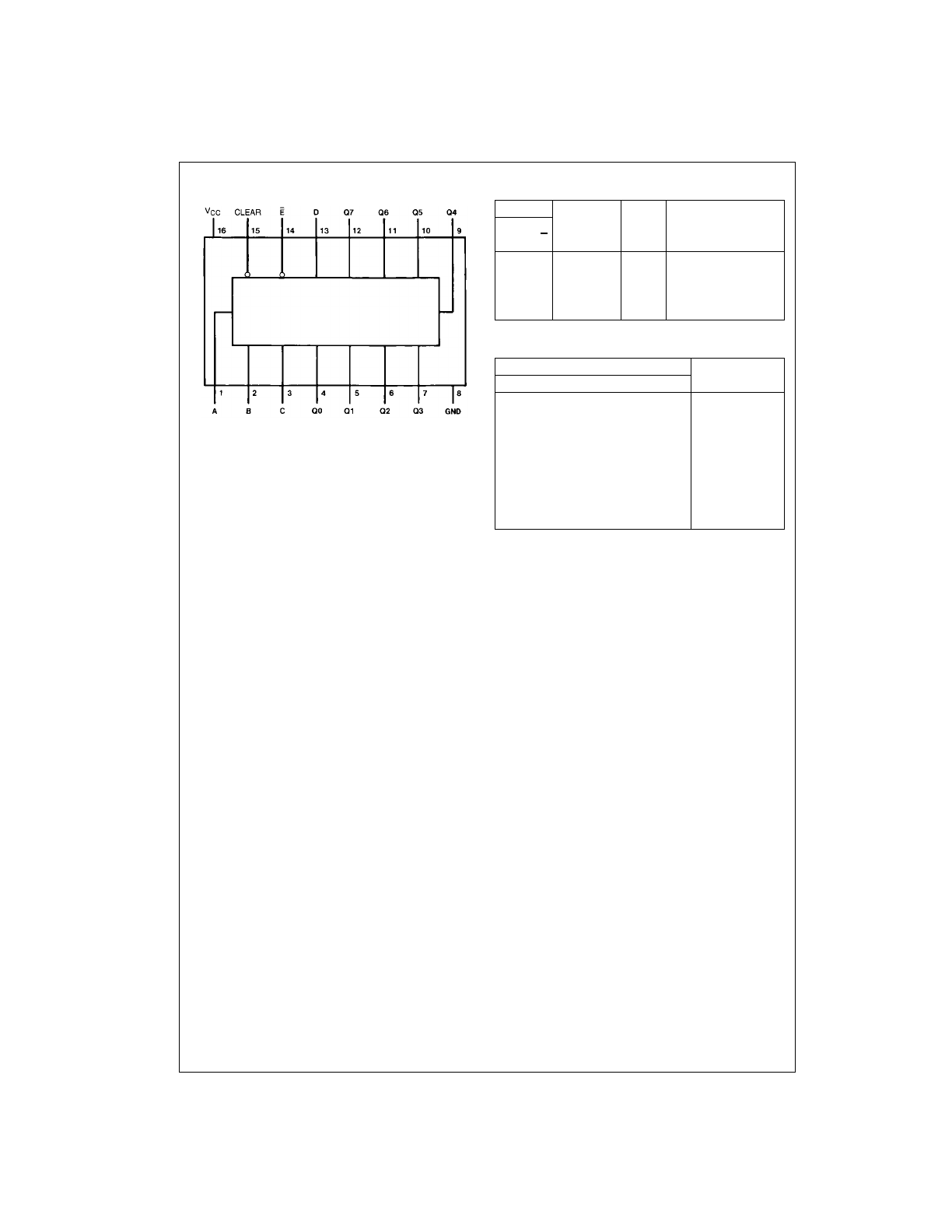
Connection Diagram
Function Table
Latch Selection Table
H
=
HIGH Level
L
=
LOW Level
D
=
the Level of the Data Input
Q
i0
=
the Level of Q
i
(i
=
0, 1,…7, as Appropriate) before the Indicated
Steady-State Input Conditions Were Established.
Inputs
Output of
Each
Addressed
Other
Function
Clear
E
Latch
Output
H
L
D
Q
i0
Addressable Latch
H
H
Q
i0
Q
i0
Memory
L
L
D
L
8-Line Demultiplexer
L
H
L
L
Clear
Select Inputs
Latch
C
B
A
Addressed
L
L
L
0
L
L
H
1
L
H
L
2
L
H
H
3
H
L
L
4
H
L
H
5
H
H
L
6
H
H
H
7
3
www.fairchildsemi.com
DM74LS259
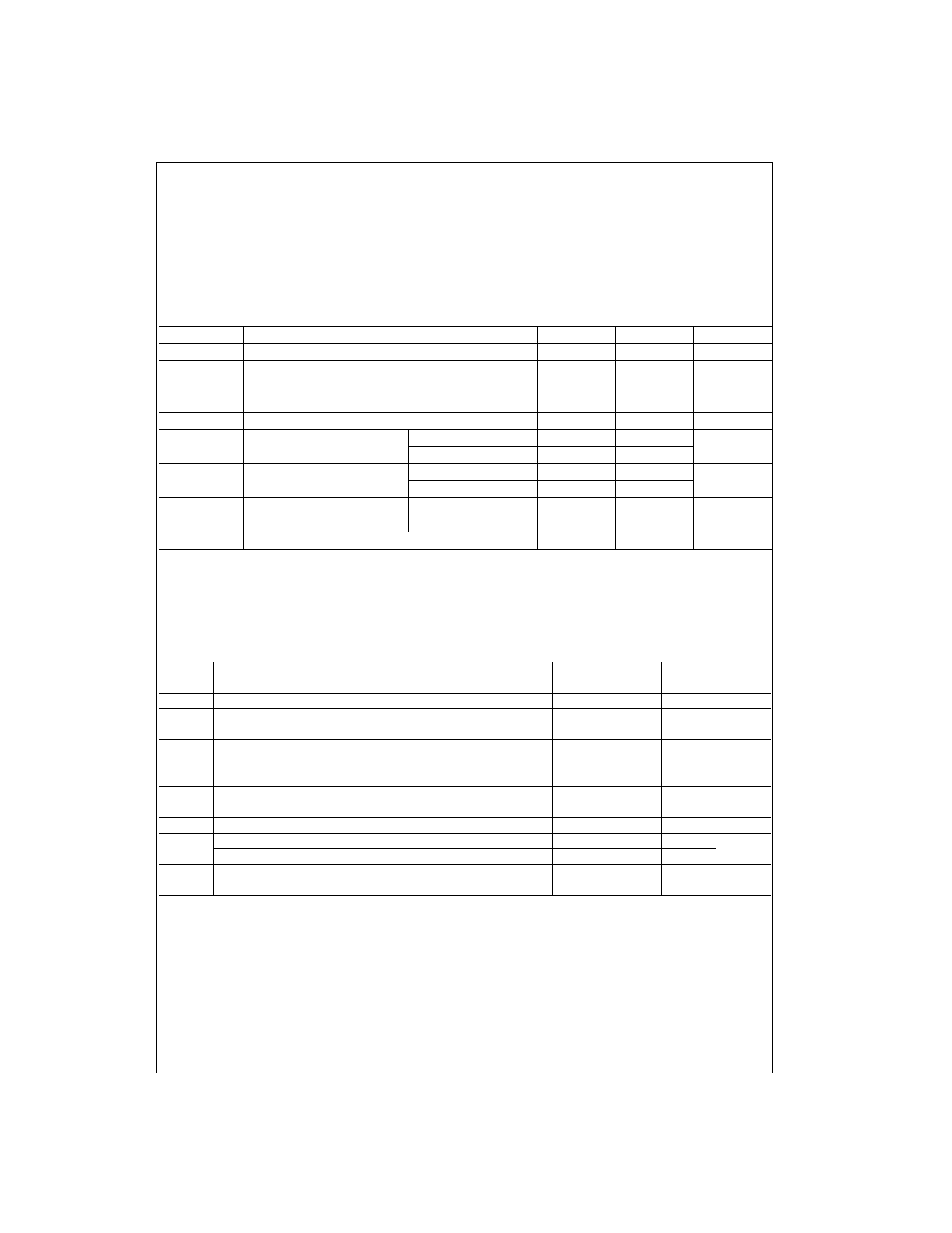
Absolute Maximum Ratings
(Note 1)
Note 1: The “Absolute Maximum Ratings” are those values beyond which
the safety of the device cannot be guaranteed. The device should not be
operated at these limits. The parametric values defined in the “Electrical
Characteristics” table are not guaranteed at the absolute maximum ratings.
The “Recommended Operating Conditions” table will define the conditions
for actual device operation.
Recommended Operating Conditions
Note 2: The symbols (
↓
,
↑
) indicate the edge of the clock pulse used for reference:
↑
for rising edge,
↓
for falling edge.
Note 3: Setup and hold times are with reference to the enable input.
Note 4: The select-to-enable setup time is the time before the HIGH-to-LOW enable transition that the select must be stable so that the correct latch is
selected and the others not affected.
Note 5: T
A
=
25
°
C and V
CC
=
5V.
Electrical Characteristics
over recommended operating free air temperature range (unless otherwise noted)
Note 6: All typicals are at V
CC
=
5V, T
A
=
25
°
C.
Note 7: Not more than one output should be shorted at a time, and the duration should not exceed one second.
Note 8: I
CC
is measured with all inputs at 4.5V, and all outputs OPEN.
Supply Voltage
7V
Input Voltage
7V
Operating Free Air Temperature Range
0
°
C to
+
70
°
C
Storage Temperature Range
−
65
°
C to
+
150
°
C
Symbol
Parameter
Min
Nom
Max
Units
V
CC
Supply Voltage
4.75
5
5.25
V
V
IH
HIGH Level Input Voltage
2
V
V
IL
LOW Level Input Voltage
0.8
V
I
OH
HIGH Level Output Current
−
0.4
mA
I
OL
LOW Level Output Current
8
mA
t
W
Pulse Width
Enable
15
ns
(Note 5)
Clear
15
t
SU
Setup Time
Data
15
↑
ns
(Note 2)(Note 3)(Note 4)(Note 5) Select
15
↓
t
H
Hold Time
Data
2.5
↑
ns
(Note 2)(Note 3)(Note 5)
Select
2.5
↑
T
A
Free Air Operating Temperature
0
70
°
C
Symbol
Parameter
Conditions
Min
Typ
Max
Units
(Note 6)
V
I
Input Clamp Voltage
V
CC
=
Min, I
I
=
−
18 mA
−
1.5
V
V
OH
HIGH Level
V
CC
=
Min, I
OH
=
Max
2.7
3.4
V
Output Voltage
V
IL
=
Max, V
IH
=
Min
V
OL
LOW
Level V
CC
=
Min, I
OL
=
Max
0.35
0.5
Output Voltage
V
IL
=
Max, V
IH
=
Min
V
I
OL
=
4 mA, V
CC
=
Min
0.25
0.4
I
I
Input Current @ Max
V
CC
=
Max, V
I
=
7V
0.1
mA
Input Voltage
V
I
=
10V
I
IH
HIGH Level Input Current
V
CC
=
Max, V
I
=
2.7V
20
µ
A
I
IL
LOW Level Input Current
V
CC
=
Max, V
I
=
0.4V
−
0.4
mA
Enable
V
CC
=
Max, V
I
=
0.4V
−
0.8
I
OS
Short Circuit Output Current
V
CC
=
Max (Note 7)
−
20
−
100
mA
I
CC
Supply Current
V
CC
=
Max (Note 8)
22
36
mA
www.fairchildsemi.com
4
DM74LS259
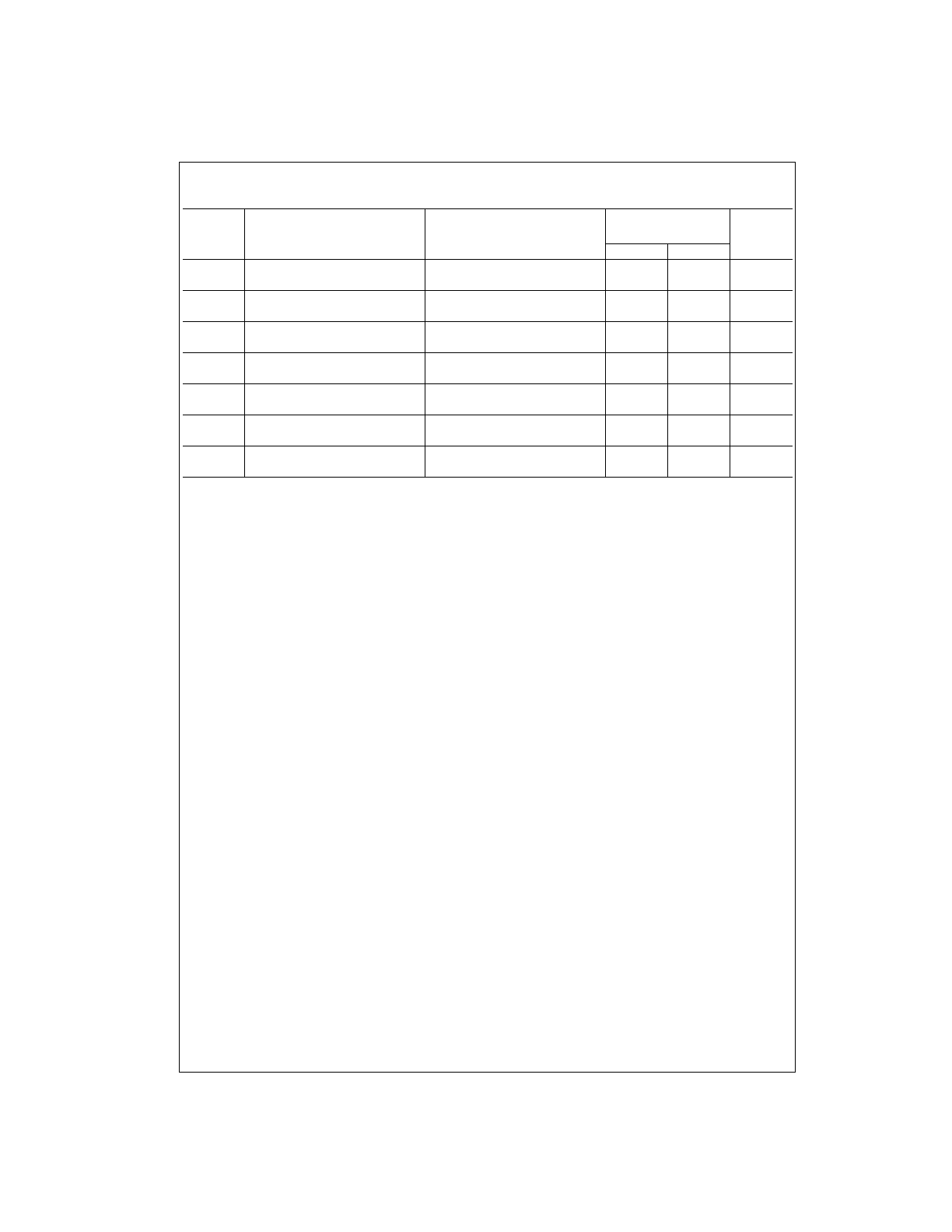
Switching Characteristics
at V
CC
=
5V and T
A
=
25
°
C
Symbol
Parameter
From (Input)
C
L
=
50 pF
Units
To (Output)
R
L
=
2 k
Ω
Min
Max
t
PLH
Propagation Delay Time
Enable to Output
38
ns
LOW-to-HIGH Level Output
t
PHL
Propagation Delay Time
Enable to Output
32
ns
HIGH-to-LOW Level Output
t
PLH
Propagation Delay Time
Data to Output
35
ns
LOW-to-HIGH Level Output
t
PHL
Propagation Delay Time
Data to Output
30
ns
HIGH-to-LOW Level Output
t
PLH
Propagation Delay Time
Select to Output
41
ns
LOW-to-HIGH Level Output
t
PHL
Propagation Delay Time
Select to Output
38
ns
HIGH-to-LOW Level Output
t
PHL
Propagation Delay Time
Clear to Output
36
ns
HIGH-to-LOW Level Output
5
www.fairchildsemi.com
DM74LS259
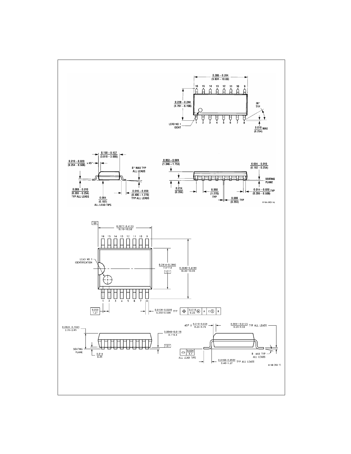
Physical Dimensions
inches (millimeters) unless otherwise noted
16-Lead Small Outline Integrated Circuit (SOIC), JEDEC MS-012, 0.150 Narrow
Package Number M16A
16-Lead Small Outline Intergrated Circuit (SOIC), JEDEC MS-013, 0.300 Wide
Package Number M16B
www.fairchildsemi.com
6
DM
7
4LS259
8
-Bit
A
d
d
ressabl
e Latches
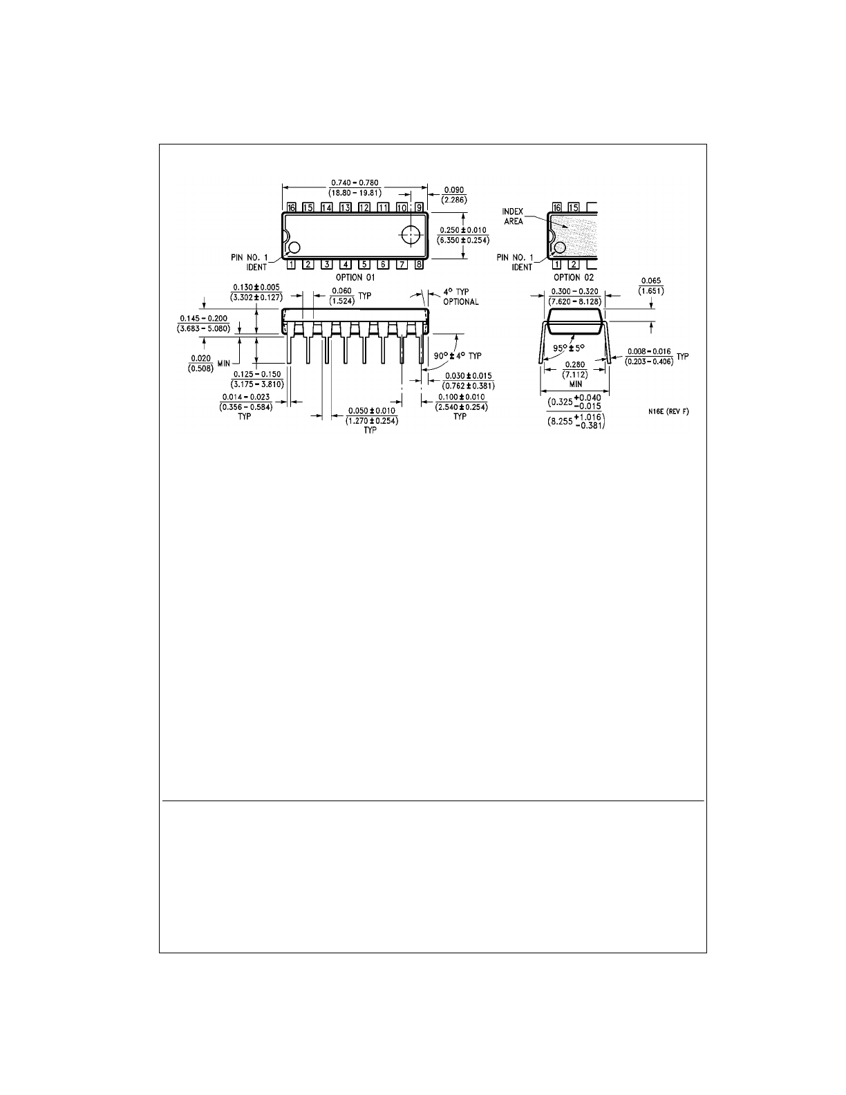
Physical Dimensions
inches (millimeters) unless otherwise noted (Continued)
16-Lead Plastic Dual-In-Line Package (PDIP), JEDEC MS-001, 0.300 Wide
Package Number N16E
Fairchild does not assume any responsibility for use of any circuitry described, no circuit patent licenses are implied and
Fairchild reserves the right at any time without notice to change said circuitry and specifications.
LIFE SUPPORT POLICY
FAIRCHILD’S PRODUCTS ARE NOT AUTHORIZED FOR USE AS CRITICAL COMPONENTS IN LIFE SUPPORT
DEVICES OR SYSTEMS WITHOUT THE EXPRESS WRITTEN APPROVAL OF THE PRESIDENT OF FAIRCHILD
SEMICONDUCTOR CORPORATION. As used herein:
1. Life support devices or systems are devices or systems
which, (a) are intended for surgical implant into the
body, or (b) support or sustain life, and (c) whose failure
to perform when properly used in accordance with
instructions for use provided in the labeling, can be rea-
sonably expected to result in a significant injury to the
user.
2. A critical component in any component of a life support
device or system whose failure to perform can be rea-
sonably expected to cause the failure of the life support
device or system, or to affect its safety or effectiveness.
www.fairchildsemi.com